Conduction Channels of an InAs-Al nanowire Josephson weak link
Abstract
We present a quantitative characterization of an electrically tunable Josephson junction defined in an InAs nanowire proximitized by an epitax-ially-grown superconducting Al shell. The gate-dependence of the number of conduction channels and of the set of transmission coefficients are extracted from the highly nonlinear current-voltage characteristics. Although the transmissions evolve non-monotonically, the number of independent channels can be tuned, and configurations with a single quasi-ballistic channel achieved.
Superconductor-semiconductor-superconductor weak links are interesting hybrid structures in which the Josephson coupling energy, and therefore the supercurrent, can be modulated by an electric field [1, 2]. It is even possible to lower enough the carrier density in the weak link to achieve the conceptually simple situation of a quantum point contact (QPC), in which only a small number of conduction channels contribute to transport. Although these kind of hybrid microstructures have been explored for many years [3], inducing strong superconducting correlations into the semiconductor in a reliable way has been achieved only recently. A well-defined (“hard”) superconducting gap has been clearly demonstrated both in InAs nanowires [4] and in In-GaAs/InAs two-dimensional electron gases [5] by using in-situ epitaxially grown Al contacts. Many experiments [6, 7, 8, 9, 10] are presently using these hybrid structures because they are promising candidates to implement topological superconductivity and Majorana bound states [11, 12]. A good understanding of their basic microscopic transport features is therefore necessary. Here we track the evolution of the conduction channels of a QPC based on an InAs-Al (core-shell) nanowire [13], as gate voltages gradually deplete the weak link region.
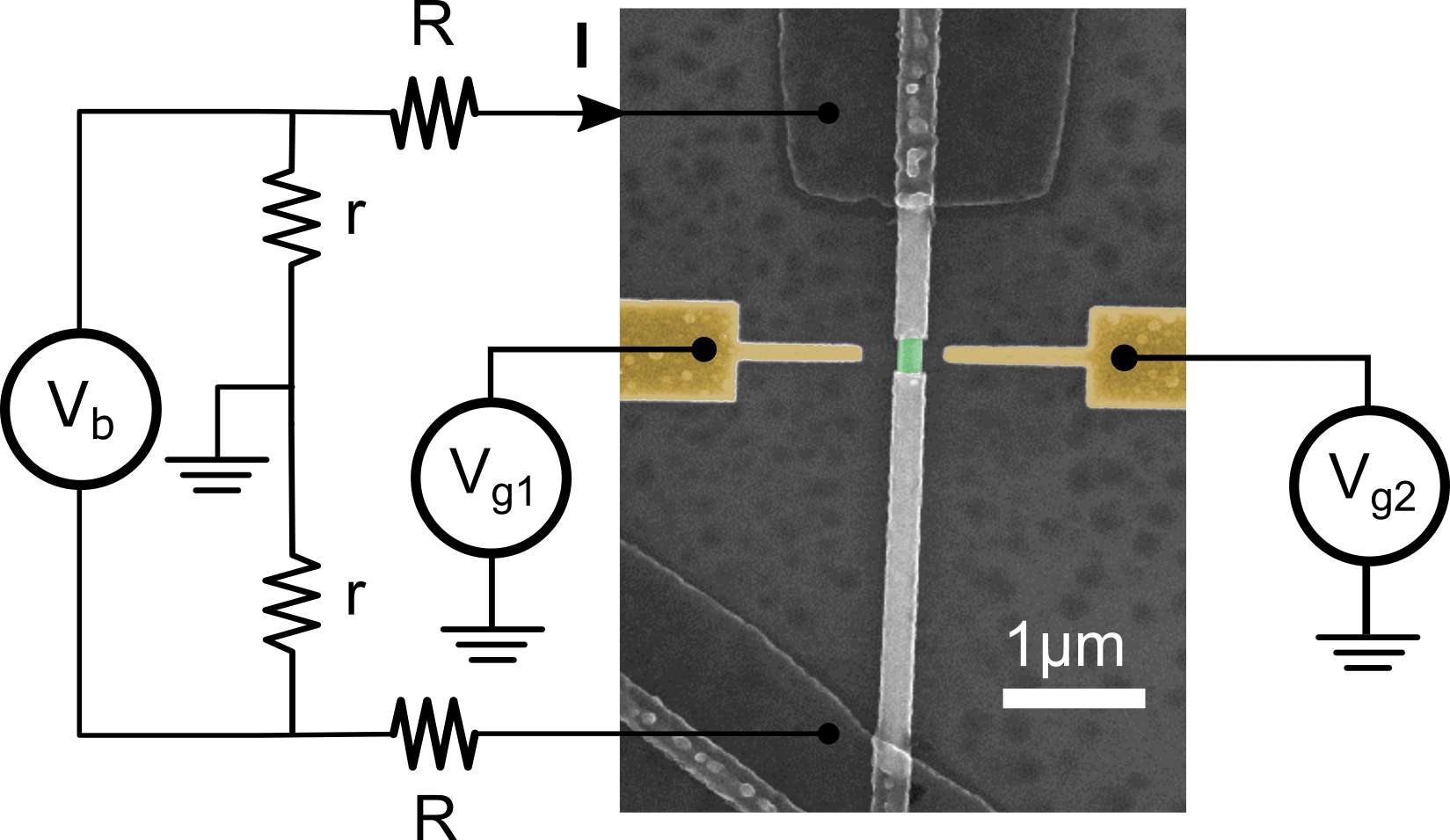
Nanowires were dispersed onto a Si substrate covered with 500 nm of silicon oxide. After an Ar ion milling step (, 90 s, nominal etch rate ), the Al shell was contacted by e-beam-evaporated 100 nm-thick micrometer-scale Al leads. The QPC was then defined by completely removing the Al shell over 150 nm by a selective wet etching step in Transene D. The etching region was defined by e-beam lithography using a PMMA layer deposited on a few-nm-thick optical resist that turns the Al-resist interface hydrophobic, hence preventing the peeling of the whole wire while etching [14]. In a subsequent lithography step, Au gates were fabricated on both sides of the exposed InAs core to allow tuning of the local carrier density. A micrograph of the device and the schematics of the measurement setup is depicted in Fig. 1. Symmetric biasing of the junction was achieved with a bridge of 4 resistances placed on the printed circuit board to which the sample is wire-bonded. The voltage V across the wire is measured with another pair of leads connected to the bias pads, whereas the current I is deduced from the voltage drop across resistance Two independent voltage sources and connected to the side-gates control the depletion of the QPC.

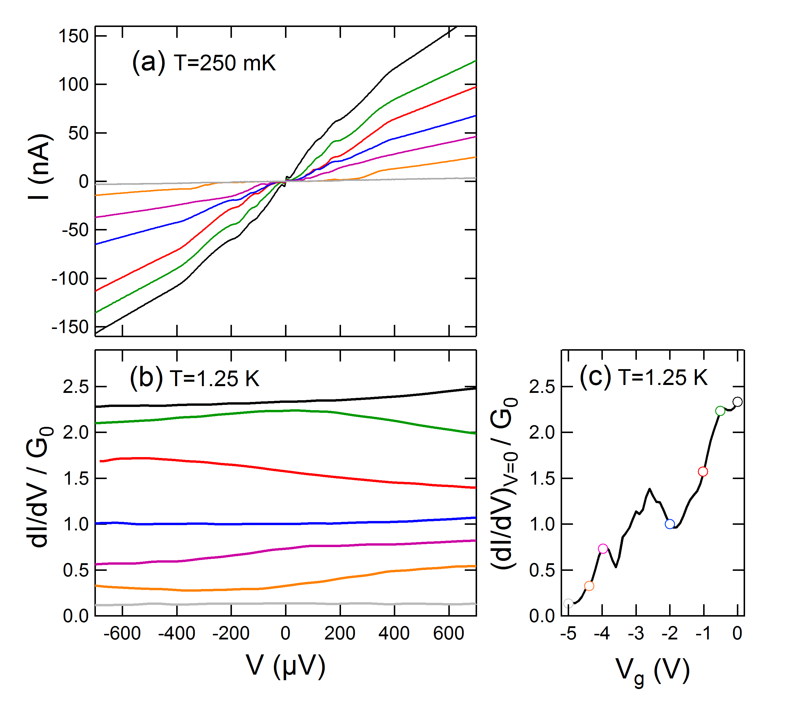
Measurements were carried out in a He3 refrigerator at a base temperature of 250 mK. Figure 2a shows I-V characteristics taken in the superconducting state at various values of the gate voltages, in the common mode =. The overall current decreases as is lowered. This correlates with the reduction of the differential conductance dI/dV in the normal state, as shown in Fig. 2b with data at the same values of taken above the superconducting transition temperature of Al. This figure also shows that dI/dV varies with V. The complete evolution with of the zero voltage conductance in the normal state is shown in Fig. 2c. The absence of conductance plateaus merely indicates that the channels do not close one after the other as decreases, in contrast to what happens with clean QPCs in two-dimensional electron gases. A detailed and comprehensive account of the evolution of all transmissions can however be obtained from the superconducting state data. The I-V characteristics in the superconducting state display kinks at voltages close to where is an integer number ( are clearly visible), is the electron’s charge, and the superconducting gap in the proximitized InAs. These non-linearities result from the charge transport occurring through Multiple Andreev Reflections (MAR) [16]. As shown by experiments on atomic contacts [17], the number of channels and the set of transmissions coefficients can be determined by decomposing the I-V characteristics into the contributions of a few channels using the well-established theory for MAR [18, 19, 20], with the gap and the transmissions as adjustable parameters. Note however that the physics is a bit richer here because, as shown in Fig. 2b, varies with and dI/dV (V)dI/dV (-V). Although the MAR theory should then in principle be modified to include the energy dependence of the transmissions, here we simply treat separately the and halves of the I-Vs and get for each gate voltage value two estimations of the set of transmissions [15].


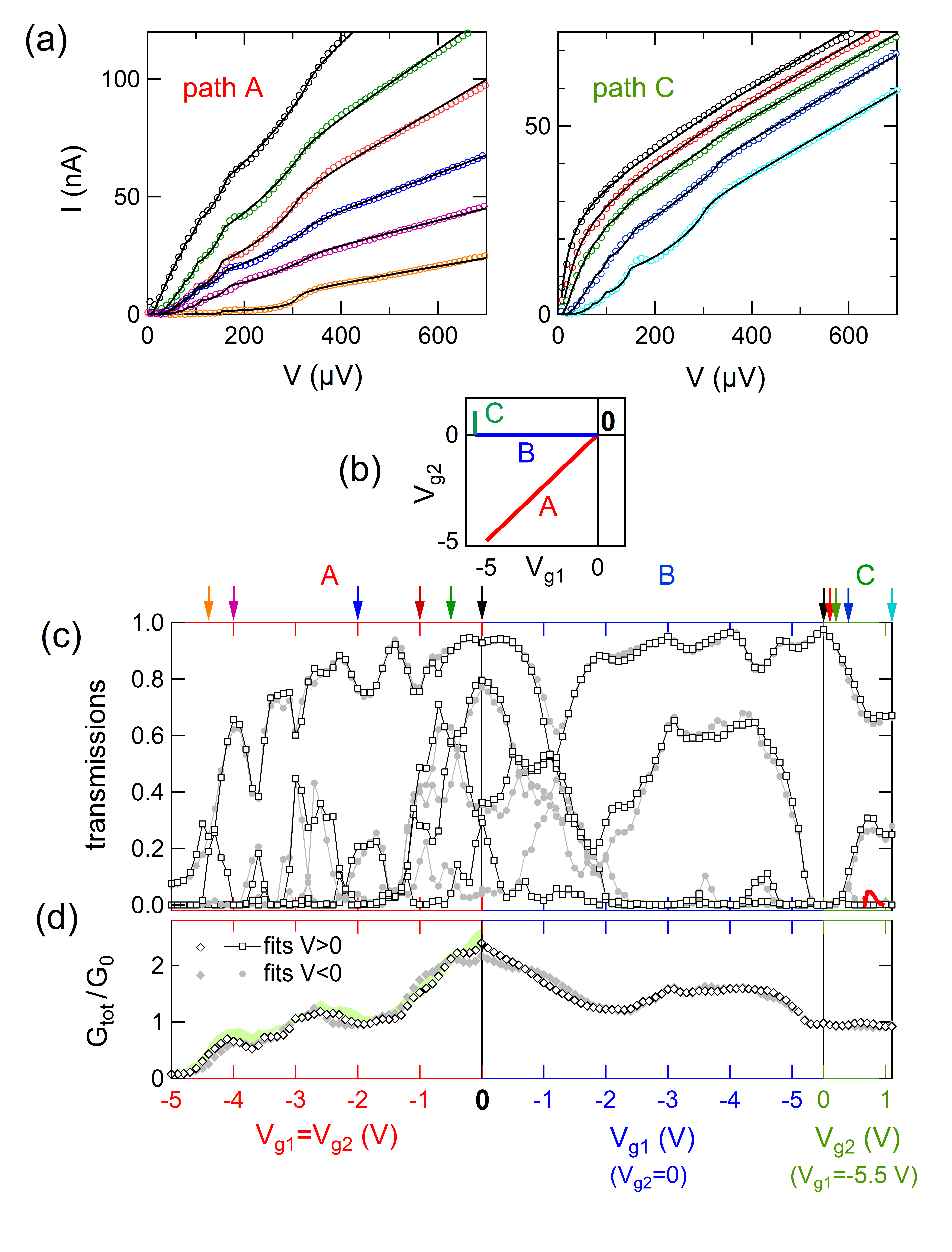
The fits, the corresponding channels’ transmissions and their sum are shown in Fig. 3a, 3c and 3d, respectively. The three panels in Figs. 3c&d correspond to data taken along the three gating paths shown in Fig. 3b. The left panel of Fig. 3a shows the fits (lines) of the data of Fig. 2a (open symbols), which are taken at gate voltages marked with arrows of the same color on leftmost panel of Fig. 3c. The right panel of Fig. 3a shows similar data taken at for 5 values of marked with arrows on rightmost panel of Fig. 3c.
According to the maximum measured normal-state conductance , one expects at least 3 independent conducting channels. Fits are performed using a Monte-Carlo algorithm described elsewhere [21]. They require at most 4 channels in the whole gate voltage range investigated. The mean value obtained for the superconducting gap is with a standard deviation of . The gap appears to be almost gate-voltage-independent, as expected from the fact that the Al shell completely covers the InAs regions that act as superconducting banks for the QPC.
Good fits with the MAR theory are obtained everywhere except near pinch-off ( and both below ), where the relative variations of dI/dV in the normal state become large. Furthermore, in this region, the current is only carried by channels with low transmission, for which the short junction limit is no longer valid: as argued in Ref. [22], additional resonances develop in the I-V when the channel is longer than , where is the superconducting coherence length in the proximitized InAs.
The evolution of the transmissions as obtained from the (full circles) and (open squares) halves of the I-Vs is shown in Fig. 3c. High transmissions are determined to a good accuracy (), whereas there is some uncertainty on lower transmissions, in particular when four channels contribute to the current. Despite the fact that the differential conductance in the normal state depends on , both determinations give very similar results. Moreover, the extracted total conductance remains mostly within the measured range of variation of the differential conductance in the normal state (see leftmost panel in Fig. 3d).
When lowering the gate voltages, the number of channels decreases from 4 to 1, although individual transmissions change non-monotonously. This behaviour is probably a consequence of impurity charges (unintentional background doping, deep charge traps in the underneath dielectric, etc.) near the InAs region giving rise to random fluctuations of the confinement potential in addition to the one defined by the split gates, as often observed in semiconducting QPCs. Note that even in the absence of disorder, a Fermi velocity mismatch between the protected and unprotected regions of the nanowire could also give rise to standing waves, leading to resonances and non-monotonicity of transmission with gate voltage.
When only a single gate voltage is decreased (gating path B), conducting channels evolve more gradually than when both are, as expected. Interestingly, at , the current flows through a single quasi-ballistic channel () (black curve in right panel of Fig. 3a). One also observes that the I-Vs change dramatically along gating path C (right panel of Fig. 3a), even though the total conductance (right panel of Fig. 3d) remains almost constant. This reveals the smooth decrease of the transmission of one channel compensating almost exactly the increase of the second one (see right panel of Fig. 3c). Similar transfer of weights are observed at several places in Fig. 3c.
In summary, we have shown that it is possible to track the conduction channels’ transmissions of an InAs nanowire superconducting QPC by measuring its current-voltage characteristics. Agreement with the MAR theory in the short-junction limit is satisfactory except very close to pinch-off. This gives confidence that following the evolution of the MAR structure with magnetic field could be a promising method to probe the topological transition predicted for such InAs nanowires [23, 24]. The information obtained on the transmissions and on the superconducting gap from the I-Vs in the superconducting state can be used to better understand spectroscopy data of the Andreev bound states (ABS) that form when phase-biasing a QPC. Finally, we find situations where transport occurs through a single channel of transmission as high as 0.98, leading to ABS energies of the order of which is favorable to probe ABS using circuit-QED techniques [25].
Acknowledgments . We thank P. Sénat and P.-F. Orfila for technical assistance, A. Levy-Yeyati for discussions and G. Rubio-Bollinger for supplying us the fitting program. We acknowledge financial support by ANR contracts MASH, JETS and by the Danish National Research Foundation.
References
- [1] G. de Lange, B. van Heck, A. Bruno, D. J. van Woerkom, A. Geresdi, S. R. Plissard, E. P. A. M. Bakkers, A. R. Akhmerov , and L. DiCarlo. Realization of Microwave Quantum Circuits Using Hybrid Superconducting-Semiconducting Nanowire Josephson Elements. Phys. Rev. Lett. 115 127002, 2015.
- [2] T. W. Larsen, K. D. Petersson, F. Kuemmeth, T. S. Jespersen, P. Krogstrup, J. Nygård , and C. M. Marcus. Semiconductor-Nanowire-Based Superconducting Qubit. Phys. Rev. Lett. 115 127001, 2015.
- [3] Thomas Schäpers. Superconductor/Semiconductor Junctions. Springer (Berlin) 2001.
- [4] Chang, W., Albrecht, S. M., Jespersen, T. S., Kuemmeth, F., Krogstrup, P., Nygård, J. , and Marcus, C. M. Hard gap in epitaxial semiconductor-superconductor nanowires. Nat. Nano. 10 232, 2015.
- [5] M. Kjaergaard, F. Nichele, H. J. Suominen, M. P. Nowak, M. Wimmer, A. R. Akhmerov, J. A. Folk, K. Flensberg, J. Shabani, C. J. Palmstrøm , and C. M. Marcus. Quantized conductance doubling and hard gap in a two-dimensional semiconductor-superconductor heterostructure. Nat. Comm. 7 12841, 2016.
- [6] S. M. Albrecht, A. P. Higginbotham, M. Madsen, F. Kuemmeth, T. S. Jespersen, J. Nygård, P. Krogstrup , and C. M. Marcus. Exponential protection of zero modes in Majorana islands. Nature 531 206, 2016.
- [7] M. T. Deng, S. Vaitieknas, E. B. Hansen, J. Danon, M. Leijnse, K. Flensberg, J. Nygård, P. Krogstrup , and C. M. Marcus. Majorana bound state in a coupled quantum-dot hybrid-nanowire system. Science 354 1557, 2016.
- [8] Eric M. Spanton, Mingtang Deng, Saulius Vaitieknas, Peter Krogstrup, Jesper Nygård, Charles M. Marcus , and Kathryn A. Moler. Current-phase relations of few-mode InAs nanowire Josephson junctions. ArXiv:1701.01188, Nat. Phys. (doi:10.1038/nphys4224) 2017.
- [9] J. Shabani, M. Kjaergaard, H. J. Suominen, Younghyun Kim, F. Nichele, K. Pakrouski, T. Stankevic, R. M. Lutchyn, P. Krogstrup, R. Feidenhans’l, S. Kraemer, C. Nayak, M. Troyer, C. M. Marcus , and C. J. Palmstrøm. Two-dimensional epitaxial superconductor-semiconductor heterostructures: A platform for topological superconducting networks. Phys. Rev. B 93 155402, 2016.
- [10] David J. van Woerkom, Alex Proutski, Bernard van Heck, Daniël Bouman, Jukka I. Väyrynen, Leonid I. Glazman, Peter Krogstrup, Jesper Nygård, Leo P. Kouwenhoven , and Attila Geresdi. Microwave spectroscopy of spinful Andreev bound states in ballistic semiconductor Josephson junctions. Nat. Phys. 13 876, 2017.
- [11] Roman M. Lutchyn, Jay D. Sau , and S. Das Sarma. Majorana Fermions and a Topological Phase Transition in Semiconductor-Superconductor Heterostructures. Phys. Rev. Lett. 105 77001, 2010.
- [12] Yuval Oreg, Gil Refael , and Felix von Oppen. Helical Liquids and Majorana Bound States in Quantum Wires. Phys. Rev. Lett. 105 177002, 2010.
- [13] P. Krogstrup, N. L. B. Ziino, W. Chang, S. M. Albrecht, M. H. Madsen, E. Johnson, J. Nygård, C. M. Marcus , and T. S. Jespersen. Epitaxy of semiconductor-superconductor nanowires. Nat. Mater. 14 400, 2015.
- [14] P. Lamarre and R. McTaggart. A positive photoresist adhesion promoter for PMMA on GaAs MESFETs. IEEE Trans. Electron Devices 37 2406, 1990.
- [15] The total current through a single channel QPC with an arbitrary energy barrier is . The analysis performed here amounts to neglecting the and dependances of the transmission.
- [16] Magnus Hurd, Supriyo Datta , and Philip F. Bagwell. Current-voltage relation for asymmetric ballistic superconducting junctions. Phys. Rev. B 54 6557, 1996.
- [17] E. Scheer, P. Joyez, D. Esteve, C. Urbina , and M. H. Devoret. Conduction Channel Transmissions of Atomic-Size Aluminum Contacts. Phys. Rev. Lett. 78 3535, 1997.
- [18] D. Averin and A. Bardas. Ac Josephson Effect in a Single Quantum Channel. Phys. Rev. Lett. 75 1831, 1995.
- [19] J. C. Cuevas, A. Martín-Rodero , and A. Levy Yeyati. Hamiltonian approach to the transport properties of superconducting quantum point contacts. Phys. Rev. B 54 7366, 1996.
- [20] V. S. Shumeiko, E.N. Bratus , and G. Wendin. Scattering theory of superconductive tunneling in quantum junctions. Low Temperature Physics 23 181, 1997.
- [21] J. J. Riquelme, L. de la Vega, A. Levy Yeyati, N. Agrat, A. Martin-Rodero , and G. Rubio-Bollinger. Distribution of conduction channels in nanoscale contacts: Evolution towards the diffusive limit. Europhys. Lett. 70 663, 2005.
- [22] Å. Ingerman, G. Johansson, V. S. Shumeiko , and G. Wendin. Coherent multiple Andreev reflections and current resonances in SNS quantum point contacts. Phys. Rev. B 64 144504, 2001.
- [23] Pablo San-Jose, Jorge Cayao, Elsa Prada , and Ramón Aguado. Multiple Andreev reflection and critical current in topological superconducting nanowire junctions. New J. Phys. 15 075019, 2013.
- [24] A. Zazunov, R. Egger , and A. Levy Yeyati. Low-energy theory of transport in Majorana wire junctions. Phys. Rev. B 94 14502, 2016.
- [25] C. Janvier, L. Tosi, L. Bretheau, Ç. Ö. Girit, M. Stern, P. Bertet, P. Joyez, D. Vion, D. Esteve, M. F. Goffman, H. Pothier , and C. Urbina. Coherent manipulation of Andreev states in superconducting atomic contacts. Science 349 1199, 2015.