Beyond Moore’s technologies: operation principles of a superconductor alternative
Abstract
The predictions of Moore’s law are considered by experts to be valid until 2020 giving rise to “post-Moore’s” technologies afterwards. Energy efficiency is one of the major challenges in high-performance computing that should be answered. Superconductor digital technology is a promising post-Moore’s alternative for the development of supercomputers. In this paper, we consider operation principles of an energy-efficient superconductor logic and memory circuits with a short retrospective review of their evolution. We analyze their shortcomings in respect to computer circuits design. Possible ways of further research are outlined.
Introduction
World’s largest chipmaker Intel “has signaled a slowing of Moore’s Law” MLD1 . The company has decided to increase the time between future generations of chips. “A technology roadmap for Moore’s Law maintained by an industry group, including the world’s largest chip makers, is being scrapped” MLD .
Three years ago Bob Colwell (former Intel chief IA-32 architect on the Pentium Pro, Pentium II, Pentium III, and Pentium IV) described stagnation of semiconductor technology in the following sentences 10 :
– Officially Moore’s Law ends in 2020 at 7 nm, but nobody cares, because 11 nm isn’t any better than 14 nm, which was only marginally better than 22 nm.
– With Dennard scaling already dead since 2004, and thermal dissipation issues thoroughly constrain the integration density – effectively ending the multicore era: “Dark Silicon” problem (only part of available cores can be run simultaneously).
The mentioned fundamental changes are most clearly manifested in supercomputer industry. Energy efficiency becomes a crucial parameter constraining its headway 1 ; 2 ; 3 . Power consumption level of the most powerful modern supercomputer Sunway TaihuLight 4 is as high as 15.4 MW. It corresponds to peak performance of 93 petaflops (1 petaflops is floating point operations per second). Power consumption level of the next generation – exaflops ( flops) supercomputers is predicted 5 to be in the sub-GW level. It is comparable to power generated by a small powerplant and results in an unreasonable bill of hundreds of million dollars per year.
Following roadmap 6 , goal power consumption level of exaflops supercomputer should be of the order of MW. It corresponds to energy efficiency of 20 pJ/flop or 50 Gflops/W. Unfortunately, energy efficiency of modern supercomputers is an order less than required. For example, the energy efficiency 4 of the Sunway TaihuLight is 6 Gflops/W. It is understood that besides other issues of exaflops computer like large space and complex cooling infrastructure, the energy efficiency makes the next step in high performance computing to be extraordinarily difficult, even with planned advances in complementary metal-oxide-semiconductor (CMOS) technology 3DP .
It is worth to mention that low energy efficiency leads to high power consumption and also limits clock frequency at the level of 4 – 5 GHz. This frequency limit occurs due to “temperature” limitations posed to integration level and switching rate of transistors. Note that cryogenic cooling of semiconductor chips will not solve the problem 8 ; 9 .
Future of high performance computing is most likely associated with one of alternative “Post-Moore’s” technologies where energy dissipation is drastically lower. It is expected that leader will be determined by 2030, while 2020 – 2030 will be the “decade of diversity”. In this paper, we consider one of the most promising candidates for leadership – the superconductor digital technology. Basic element switching energy here is of the order of J, with no penalty for signal transfer. For a certain algorithm superconducting circuits were shown to be up to seven orders of magnitude more energy efficient than their semiconductor counterparts, including power required for cryogenic cooling AQFPrec . Maturity level of superconductor technology can be illustrated by the notional prototype of the superconducting computer being developed under IARPA programm “Cryogenic computing complexity” C3 . This is a 64 bit computing machine operating at 10 GHz clock frequency with throughput of bit-op/s and energy efficiency of bit-op/J at 4 K temperature. Prospective study shows that superconductor computer could outperform its semiconductor counterparts by two orders of magnitude in energy efficiency, showing Gflops/W Holmes .
Purpose of this paper is a review of superconducting logic and memory circuits principles of operation and analysis of their issues in respect to computer circuits design. We certainly do not claim to be comprehensive while considering only the most common solutions. Our review contains two main parts describing logic and memory, correspondingly.
In the first part we start with examination of physical basis underlying logic circuits operation. Superconductor logics are presented by two main branches: digital single flux quantum (SFQ) logics and adiabatic superconductor logic (ASL). Basic principles of SFQ circuits operation are shown on example of the most popular rapid single flux quantum (RSFQ) logic. It’s energy efficient successors and competitor, LV-RSFQ, ERSFQ, eSFQ and reciprocal quantum logic (RQL), are considered subsequently. ASL is described in the historical context of its development for ultra energy efficient reversible computation. The modern status is presented by two implementations of this logic. It can be noted that superconducting adiabatic cells are used also in quantum computer circuits like the ones fabricated by D-Wave Systems.
The second part of the review is devoted to cryogenic memory. Four approaches are described: SQUID-based memory, hybrid Josephson-CMOS memory, Josephson magnetic random access memory (JMRAM), and orthogonal spin transfer magnetic random access memory (OST-MRAM). They are presented in historical order of their development. In the end of each part of our review we briefly discuss major challenges and directions of possible further research in the studied area.
Review
I Logic
I.1 Physical basis underlying logic circuits
The fundamental physical phenomena underlying superconducting logic circuits operation is the superconductivity effect, the quantization of magnetic flux and the Josephson effects. The first one enables ballistic signal transfer not limited by power necessary to charge capacitance of interconnect lines. It provides the biggest advantage in energy efficiency in comparison to conventional CMOS technology. Indeed, superconducting microstrip lines are able to transfer picosecond waveforms without distortions with speed approaching the speed of light, for distances well exceeding typical chip size, and with low crosstalk LSmsl . This is the basis for fast long-range interactions in superconducting circuits.
Note that absence of resistance () leads to absence of voltage () in a superconducting circuit in stationary state. Superconducting current flow corresponds not to electrical potentials difference (the voltage ) but to difference of superconducting order parameter phases , accordingly. Superconducting order parameter corresponds to superconducting electrons wave function in Ginzburg – Landau theory GL . Magnetic flux in a superconducting loop of inductance provides an increase of superconducting phase along the loop and results in permanent circulating current . This ratio is analogous to Ohm’s law . It allows to write linear Kirchoff equations for superconducting circuits.
The quantization of magnetic flux introduces fundamental difference between CMOS and superconducting circuits operation. It follows from uniqueness of superconducting electrons wave function. Indeed, increase of superconducting phase along a loop corresponds to magnetic flux as (where Wb is the magnetic flux quantum, is the Planck constant, and is the electron charge). Fulfillment of this relation is possible if (where is integer) and therefore . Magnetic flux in a superconducting loop can take only values multiple to the flux quantum, accordingly.
Physical representation of information is typically based on the quantization of magnetic flux. For example, presence or absence of SFQ in a superconducting loop can be considered as a logical unity “1” or zero “0”. Note that information is physically localized due to such representation. This is a fundamental difference compared to information representation in semiconductor circuits. The localization leads to deep analogy between superconducting logic cells and von Neuman cellular automata LSmsl where short-range interactions are predominant.
The nonlinear element in superconducting circuits is the Josephson junction. It is a weak link between two superconductors, e.g., the most used superconductor-isolator-superconductor (SIS) sandwich. One of the most important Josephson junction parameters is its critical current, . This is the maximum superconducting current capable of flowing through the junction. Josephson junction can be switched from superconducting to resistive state by increasing the current above . Transition to resistive state allows to change magnetic flux in a superconducting loop, and hence to perform a digital logic operation.
Dynamics of SIS junction is commonly described in the frame of the resistively shunted junction model with capacitance (RSJC) RSJC . This model presents Josephson junction as a parallel connection of the junction itself transmitting superconducting current, , only, a resistor and a capacitor with corresponding currents, and , where is time. The total current through the junction is the sum, . This model is based on DC and AC Josephson effects which determine the superconducting current and voltage .
The DC Josephson effect describes the superconducting current-phase relation (CPR). For SIS junction it is , where is the superconducting order parameter phase difference across the Josephson junction. It is called the Josephson phase. By presenting the relation between superconducting order parameter phase and magnetic flux as , we note that CPR couples current with the magnetic flux in a superconducting loop. Josephson junction acts as a nonlinear inductance in the circuits, accordingly.
The AC Josephson effect binds the voltage on Josephson junction in resistive state with the superconducting phase evolution as . According to this relation, increase of the Josephson phase in is accompanied by appearance of the voltage pulse across the junction such that . Therefore, a single switching of the Josephson junction into resistive state corresponds to transmission of SFQ pulse through the junction. The energy dissipated in the switching process is J, taking typical mA. The typical critical current value is conditioned by working (liquid helium) temperature, K. For proper circuits operation it should be about three orders higher than the effective noise current value, A, where is the Boltzmann constant.
Characteristic frequency of the Josephson junction switching process is determined by Josephson junction parameters, , where product is the Josephson junction characteristic voltage, and is the junction resistance in the normal state. Since SIS junctions possess large capacitance, they are usually shunted by external resistors to avoid -resonances. The resistance is approximately equal to resistance of the shunt because is much smaller than own tunnel junction resistance. For Nb-based junctions the characteristic frequency is of the order of GHz (the characteristic voltage is at the level of mV). Superconducting digital circuits are predominantly based on tunnel junctions because of high accuracy of their fabrication process and high characteristic frequencies.
By expressing the currents , and of RSJC model through the Josephson phase , we can present the total current flowing through the junction in the following form:
| (1) |
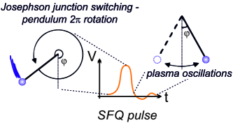
where is the Stewart-McCumber parameter reflecting capacitance impact, and dot denotes time differentiation. This Equation 1 is quite analogous to the one for mechanical pendulum with the moment of inertia (capacitance here is analogous to mass), the viscosity factor (resistance determines damping), and the applied torque . This simple analogy allows to consider superconducting digital circuit as a net of coupled pendulums.
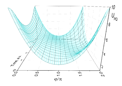
Pendulum rotation is accompanied by subsequent oscillations around stable equilibrium point (Figure 1). In Josephson junction dynamics they are called “plasma oscillations”. Plasma oscillations frequency is . For proper logic cell operation these oscillations should vanish before subsequent Josephson junction switching. Compliance with this requirement can be achieved with , . Clock frequency is accordingly less than , and is under GHz in practical circuits.
Complexity of a superconducting circuit realizable on a chip is determined by Josephson junction dimensions. Area of Josephson junction is closely related to its critical current density, . This parameter is one of the most important in the standard Nb-based tunnel junction fabrication process. It is fixed by material properties of insulating interlayer Al2O3 between superconducting Nb electrodes, and its thickness nm. The critical current density value lies typically in the range A/m2. The corresponding Josephson junction specific capacitance is fF/m2. Variation in Josephson junction critical current, , is obtained by variation of its area, . It is accompanied by variation of Josephson junction capacitance, . The shunt resistance is adjusted in accordance with the mentioned condition, , as . Its area is defined by Josephson junction area , minimum wiring feature size T ; HYPDL ( m), and sheet resistance of used material ( per square for Mo or MoNx) T ; HYPDL .
While own Josephson junction weak link area is typically m2 for A/m2, its total area with the shunt is by an order lager. Corresponding Josephson junctions available density on a chip is cm2. Superconducting circuit complexity becomes limited to million junctions per cm2 nowadays under assumption that only a quarter of chip area can be occupied by Josephson junctions (with taking interconnects into account) T . The circuit can be further expanded using multi-chip module (MCM) technology MCM1 ; MCM2 .
I.2 Digital SFQ logics
I.2.1 SFQ circuit basic principles of operation
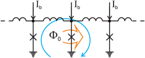
Data processing in SFQ circuits can be discussed on an example of RSFQ cells operation. RSFQ data bus is shown in Figure 2. It is a parallel array of superconducting loops composed of Josephson junctions (shown by crosses) and superconducting inductances. This structure is called the Josephson transmission line (JTL). SFQ can be transferred along this JTL by successive switchings of Josephson junctions. The switching is obtained by summing the SFQ circulating current and the applied bias current . Josephson junction transition into resistive state leads to SFQ circulating current redistribution toward the next junction. The redistribution process ends by the next junction switching and successive returning of the current junction into the superconducting state.
This example shows the basic principle of SFQ logic cells operation. It reduces to summation of currents, which are SFQs currents and bias currents. This summation leads (or not leads) to successive Josephson junction switching resulting in reproduction (or not reproduction) of SFQ. In RSFQ convention LSmsl ; 20 arrival of an SFQ pulse during clock period to a logic cell has a meaning of binary “1”, while absence of the one means “0”.
Figure 3 illustrates an example of clocked readout of information from a RSFQ logic cell. Clocking is performed by means of SFQs application to the cell. Upper JTL in Figure 3 serves for SFQ clock distribution. SFQs are allotted to the cell through extra branch coupled to the JTL as shown. Note that Josephson junction clones SFQ at the branch point. Readout operation is performed by a couple of junctions marked by dotted rectangle. This couple is commonly called the decision making pair. Existence (or absence) of an SFQ circulating current in the logic cell loop makes the lower junction to be closer (or father) to its critical current compared to the upper junction. Clocking SFQ switches the lower (or upper) junction, correspondingly. SFQ reproduction by the lower junction means logical “1” to the output, while SFQ absence from the ones means logical “0”.
One can note a couple of typical SFQ circuits features from the presented example. Considered logic cell acts as a finite state machine. Its output depends on a history of its input. This particular cell operates as a widely used D flip-flop (“D” means “data” or “delay”) – the basis of shift registers. Note that its realization is much simpler than the one of semiconductor counterparts. RSFQ basic cells are such flip-flops, and therefore RSFQ is sequential logic. This is in contrast with semiconductor logic which is combinational one (where logic cell output is a function of its present input only).
Since only one clocked operation is performed during a clock period (some operations can be performed asynchronously), a processing stage in RSFQ circuits is reduced to a few logic cells. This is also completely opposite to conventional semiconductor circuits.
I.2.2 RSFQ logic
RSFQ logic dominates in superconductor digital technology since 1990-s years 17 . Many digital and mixed signal devices like analog-to-digital converters OM_ADC ; OM_ADC1 , digital signal and data processors M_DCRev were realized on its basis.
Unfortunately, energy efficiency did not matter in the days of RSFQ development. High clock frequency was thought to be the major RSFQ advantage in the beginning. Extremely fast RSFQ-based digital frequency divider 18 (T flip-flop) was presented just about a decade later RSFQ invention. Its clock frequency was as high as GHz. It is still among fastest ever digital circuits.
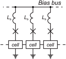
The first RSFQ basic cells were the superconducting loops with two Josephson junctions (commonly known as the superconducting quantum interference devices - SQUIDs). These cells were connected by resistors 20 ; 19 (so “R” was for “resistive” in the abbreviation). Power supply bus coupling was also resistive. While resistors connecting the cells were rather quickly substituted for superconducting inductances and Josephson junctions RSFQind , the ones in feed lines remained until recent years, see Figure 4. They determined stationary energy dissipation, , where and are the DC bias current and according voltage. The bias current is typically . The bias voltage had to be an order higher than the Josephson junction characteristic voltage, , to prevent the bias current redistribution. This requirement determined the bias resistors values. Typical RSFQ cell stationary power dissipation 8 is nW.
Another mechanism providing power dissipation corresponds to Josephson junction switching. This dynamic power dissipation is defined as , where is the clock frequency. For a typical clock frequency of 20 GHz is at the level 8 of nW. It is seen that the dynamic power dissipation is about 60 times less than the stationary one. Main efforts to increase RSFQ circuits energy efficiency were aimed at stationary energy dissipation decrease, accordingly. RSFQ energy efficient successors, LV-RSFQ, ERSFQ and eSFQ, are presented below.
I.2.3 LV-RSFQ
The first step toward reduction was the bias voltage decrease. Bias current redistribution between neighboring cells in low-voltage RSFQ (LV-RSFQ) is damped by introduction of inductances connected in series with bias resistors in feed lines 23 ; 24 ; 25 ; 26 ; 261 .
Unfortunately, this approach limits clock frequency. Indeed, clock frequency increase is accompanied by increase of average voltage across a cell (according to the AC Josephson effect). This in turn leads to bias current decrease proportional to . The latter finally results in the cell malfunction RL . This tradeoff with requirement of additional circuit area for inductances in feed lines practically limit application of this approach. Since static power dissipation is not eliminated, this is somewhat half-hearted solution. It was succeeded by another two RSFQ versions (ERSFQ and eSFQ, where “E/e” stays for “energy efficient”) where is totaly zero.
I.2.4 ERSFQ
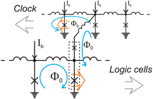
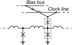
ERSFQ 27 is the next logical step after LV-RSFQ. Resistors in feed lines are substituted for Josephson junctions limiting bias current variation in this logic, see Figure 5. This replacement is somewhat analogous to the one which was done for resistors connecting SQUID cells in the very first RSFQ circuits. It provides possibility for the circuits to be in pure superconducting state.
Main difficulty in the bias resistors elimination is formation of superconducting loops between logic cells. Generally, logic cells are switched asynchronously depending on processing data. Average voltage and total Josephson phase increment are different across them. This results in emergence of currents circulating through neighbor cells. Being added to bias current, these currents prevent correct operation of the circuits.
Imbalance of Josephson phase increment is automatically compensated by corresponding switchings of Josephson junctions placed in ERSFQ feed lines. Since these switchings are not synchronized with clock, some immediate alteration of bias current is still possible. This alteration is limited by inductance connected in series with Josephson junction in the feed line. While large value of this inductance minimizes the bias current variation, its large geometric size increases the circuit area (similar to LV-RSFQ). Possible solutions of this problem are an increase of wiring layers number, and utilization of superconducting materials having high kinetic inductance. These materials can be also used for further miniaturization of logic cells themselves T .
I.2.5 eSFQ
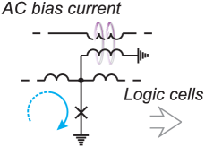
Another energy efficient logic of RSFQ family is eSFQ 8 ; 28 ; 32 ; 33 . The main idea here is the “synchronous phase balancing”. Bias current is applied to decision making pair, see Figure 6. One Josephson junction of this pair is always switched during a clock cycle regardless data content. Therefore, average voltage and Josephson phase increment are always equal across any such pair. This prevents the emergence of parasitic circulating currents. Josephson junction in the feed line is required only for proper phase balance adjustment during power-up procedure. “It is not expected to switch during regular circuit operation” 8 .
Achieved phase balance allows to eliminate large inductances from ERSFQ feed lines, and so eSFQ circuits occupy nearly the same area as RSFQ ones. One should note that despite of the “synchronous” nature of this logic, a method for design of eSFQ-based asynchronous circuits was proposed in 32 , making it suitable for wave-pipelined architecture.
Since RSFQ library was designed regardless synchronous phase balancing, transition to eSFQ requires its correction. In some cases it leads to increase of Josephson junctions number. For example, JTL should be replaced by a shift register 29 or by “Wave JTL” 32 , or by one of its asynchronous counterparts: ballistic transmission line based on unshunted Josephson junctions 30 ; 31 or passive microstrip line.
Similarity of ERSFQ and eSFQ approaches allows to make an overall assessment of total increase in Josephson junctions number up to % compared to RSFQ circuits 8 . Inheritance of basic cells design of RSFQ by ERSFQ makes it easier to use.
I.2.6 RSFQ logic family common features
Clock is effectively a part of data in ERSFQ circuits. This means that they are globally asynchronous.
Since clock frequency is determined by repetition rate of SFQs in clocking JTL, it can be adjusted “in flight” by logic cells according to processing data.
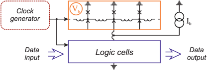
The bias voltage source can be implemented as a JTL fed by a constant bias current, for which the input signal is the SFQ clock applied from an on-chip SFQ clock generator, see Figure 7. Average voltage on this JTL is precisely proportional to the clock frequency, , according to the AC Josephson effect. Clock control by logic cells allows to adjust this voltage or even to turn it off. The last option corresponds to circuits switching into “sleep mode” where power dissipation is totally zero. Realization of this power save mechanism at individual circuits level is possible with circuits partitioning into series connection of islands with equal bias current but different bias voltage T_RSFQ_SB .
Since logic cells are fed in parallel in RSFQ logic family, total bias current increases proportional to Josephson junctions number. For 1 million Josephson junctions the bias current value could be unreasonably high A. Circuits partitioning allows to keep it at acceptable level Jap_HS_SFQ below A.
I.2.7 RQL
RQL was proposed in about 2008. It was developed as an alternative to conventional RSFQ, and presented as “ultra-low-power superconductor logic” 14 . Main difference between RQL and RSFQ is in the way of power supply RQL . While in RSFQ it is a DC power applied to Josephson junctions in parallel through bias resistors (Figure 4), in RQL it is an AC power applied in series through bias transformers, see Figure 8.
The proposed power supply scheme possesses some advantages. (i) No DC bias current and no bias resistors means zero static power dissipation inside cryogenic cooler. Bias current is terminated off chip at room temperature. (ii) The well known RSFQ circuits design problem is the large return bias current magnetic field affecting logic cells. It is recommended Jap_HS_SFQ to keep maximum bias current below mA in RSFQ feed line. This return current is completely absent in RQL due to the mentioned off-chip bias current termination. (iii) Serial bias supply allows to keep bias current amplitude at fairy low level 14 of the order of mA regardless number of Josephson junctions on a chip. There is no need for the large-scale circuit partitioning. (iv) Bias current plays a role of clock signal. There is no need for SFQ clock distribution network. (v) Clock is not affected by thermal noise.
Logical unity (zero) is presented by a pair of SFQs having opposite magnetic flux directions (or lack thereof) in RQL circuits. These SFQs can be transferred in one direction with application of inversely directed bias currents, see Figure 9. The SFQs are placed in positive/negative AC current wave half period, accordingly. Unfortunately, one AC bias current is insufficient for directional propagation of the SFQs. It can provide only periodic space oscillations of the flux quanta. RQL uses two AC bias currents with phase shift. RQL cells are coupled to these two feed lines in rotation (Figure 9). Such coupling produces space division of total bias current/clock into four windows shifted by , , , and wave period. By analogy with a car’s four-stroke engine, this four-phase bias scheme provides directionality of the SFQs propagation 14 .
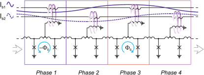
Logic elements connected to a single AC bias line within a single clock phase window form a pipeline. The pipeline in RQL can contain an arbitrary number of cells. One can increase a depth of the pipeline at the cost of clock frequency decrease. Time delay of the pipeline should be less than one-third of clock period for proper circuit operation. Circuit speed is effectively a product of clock frequency and pipeline depth. Maximum clock frequency of RQL circuits can be estimated as GHz under assumption of the standard Josephson junction characteristic frequency GHz and Josephson junctions in the pipeline RQL .
RQL biasing scheme provides self data synchronization. Early pulses wait at the pipeline edge for bias current rise in the next phase window. SFQ jitter is accumulated only inside one pipeline, and therefore timing errors are negligible which is in contrast to RSFQ.
RQL logic cells are state machines similar to RSFQ ones. Internal state of logic cell can be changed by SFQ propagating in front of the clock wave. Its paired SFQ with opposite polarity serves for the state resetting in the end of a clock period.
Complete set of RQL logic cells comprises just three gates which are And-Or gate, A-not-B gate and Set-Reset latch. These gates behave as combinational logic cells similar to their semiconductor counterparts RQL . This makes RQL circuits design to be closer to CMOS than to RSFQ.
Particular RQL drawbacks come from power supply scheme as well as its advantages. Proper power supply requires high-frequency power splitters. These splitters often occupy quite a large area. For example, in implementation of 8-bit carry-look-ahead adder they cover area times larger than the adder itself RQL_adder . One can note that power supply through transformers also limits the possibility for the circuits miniaturization.
Multiphase AC bias presents known difficulty for high-frequency design (clock skew etc.). This practically limits clock frequency to GHz, while RSFQ circuits routinely operate at frequency of GHz. Moreover, implementation of MCM technology becomes complicated with RQL due to possible asynchronization of chips or clock phase shift. Besides inconvenience presented by high-frequency clock supply from off-chip external source, clocking by AC bias currents eliminates possibility of clock control by logic cells. Corresponding power save mechanisms cannot be realized in RQL. In addition, one should mention RF losses in microstrip resonators which typically make up to 50% total power budget even at relatively low frequencies.
Total power dissipation of RQL and ERSFQ circuits in active mode seems similar. Static power dissipation is absent. Dynamic power dissipation is associated with Josephson junction switching in data propagation process. In RQL circuits Josephson junction is doubly switched for logical unity transfer and zero times for transfer of logical zero. In ERSFQ both unity and zero are transferred with switching of one of the Josephson junctions in decision making pair. By assuming equal number of zeros and ones in data, one comes to roughly equal estimation for energy dissipation in both RQL and ERSFQ logics T . More detailed analysis shows that only adiabatic switching of logic cells improves superconducting circuits energy efficiency markedly T .
I.3 Adiabatic superconductor logic
Considered variants of superconductor logics have been proposed for non-adiabatic irreversible computation. Logical states are separated here by energy barrier ensuring proper circuit operation. Note that the energy barrier in semiconductor circuits is two to three orders higher, . Minimal energy barrier corresponds to Landauer’s “thermodynamic limit”, 40 . In this limit logic states distinguishability becomes completely lost due to thermal fluctuations 9 .
Energy required to perform a non-adiabatic logic operation can be estimated as the energy of transition between logical states corresponding to . In considered superconductor logics it is the energy of Josephson junction switching, J. While presuming logical irreversibility, this energy can be lowered down to J (at K) by using adiabatic switching process. Note that Landauer limit in this context reflects computing system entropy change associated with an irreversible operation 40 . At the same time, there is no such limit for physically and logically reversible process. Therefore, energy dissipated per logical operation can approach zero in adiabatic reversible circuits.
The first ever practical reversible logic gates were realized recently 48 on a basis of adiabatic superconductor logic. History of ASL development have begun even before RSFQ invention with proposition of “parametric quantron” PQ in 1976. This cell itself was proposed even earlier in 1954 as “rf parametron” rfP , though for different operating regime.
It is interesting to note that the manner of parametric quantron cell operation was implemented later in a single-electron device 17 ; QCA1 in 1996. The “single-electron parametron” operation was in fact quite similar to the ones of quantum-dot cellular automata (QCA) which were proposed for computation those years QCA2 .
I.3.1 ASL circuit basic principles of operation
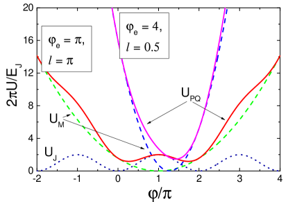
Parametric quantron is a superconducting loop with single Josephson junction shown in Figure 10 leftward. Its state is conditioned by external magnetic flux, , and current, , controlling Josephson junction critical current . Potential energy of this cell is a sum of Josephson junction energy, (followed directly from the DC Josephson effect), and magnetic energy, :
| (2) |
where , is the normalized loop inductance.
It is seen that external parameters , control vertex (through ) and slope (through ) of the potential energy parabolic term in Equation 2. Under appropriate bias flux, , parametric quantron potential energy can take single-well (at ) or double-well (at ) shape depending on , see Figure 11. Logical zero and unity can be represented by the cell states with Josephson junction phase lower or higher than . For these states correspond to minima of potential wells. Physically they correspond to different magnetic flux in the loop (with current circulating in the loop in opposite directions if , where is integer).
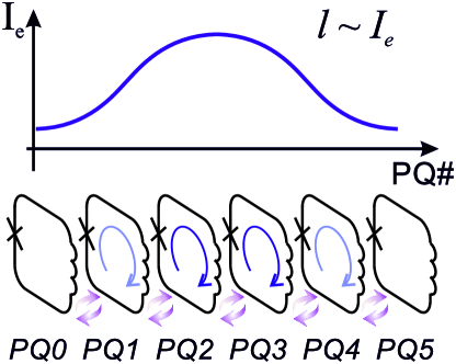
Logical state transfer can be performed in array of magnetically coupled parametric quantrons biased into working point . Current pulse should be applied sequentially to the cells increasing their normalized inductance one by one, see Figure 12. Logical state can be shared by a group of cells, wherein it is most pronounced in a cell with the largest in particular moment. Dynamics of this transfer process can be made adiabatic by adjusting the shape of the driving current pulse . Cross-coupling of the cells enables adiabatic reversible logic operations LikhPQ .
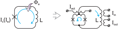
Single Josephson junction of parametric quantron was substituted by SQUID (see Figure 10 rightward) in practical implementations Convolv . Activation current, , here plays a role similar to the ones of . It induces circulating current in activation SQUID, and therefore increases Josephson junctions phases, according to the DC Josephson effect. This in turn corresponds to increase of Josephson junctions energy which can be minimized with appearance of current circulating in the main parametric quantron loop (the loop containing inductance ). However, the states with both directions of the circulating current are equally favorable due to symmetry of the scheme. Choice of one of these states corresponds to direction of input current playing here the role of . Due to the fact that current-less state is unstable balance corresponding to potential energy local maximum, the current can be infinitesimally small. Parametric quantron can provide virtually infinite amplification of magnetic flux, accordingly. Since potential energy minimum is achieved with circulating currents in both: activation SQUID and main parametric quantron loop, it was noted that the roles of the activation and the input/output can be swapped QFP .
Unfortunately, already the first designs in mid 1980-s of physically and logically reversible parametric quantron based processor Convolv showed this approach to be impractical. The reason for such conclusion was as follows. Logical reversibility can be achieved by temporary storage of all intermediate results BenLR . Together with predominance of short-range interactions this produces severe hardware overhead. Indeed, realization of 8-bit 1024-points fast convolver required almost parametric quantrons Convolv . About 90% of them were operated just as elements of shift registers, transferring data through the processor Convolv . It was noted that such circuits are also featured by low speed (in comparison to RSFQ) and low tolerance to parameters variations 17 .
I.3.2 Quantum flux parametron based circuits
Few years later the works on reversible circuits, the same principles of operation were utilized for development of generally non-reversible Josephson supercomputer. In this effort parametric quantron was renamed as “quantum flux parametron” (QFP) QFP . The major problem of QFP-based circuits was high-frequency multi-phase AC power supply (which was later borrowed by RQL). While there were different approaches elaborated for its solution QFP ; QFP1 , finally multi-phase AC biasing was recognized to be intractable obstacle for implementation of complex high-clock-frequency practical circuits and QFP-based approach was abandoned for some years.
Renewed interest to ASL was introduced by development of superconductor quantum computer. QFPs are utilized as qubits and couplers in adiabatic quantum optimization systems of D-Wave Systems DWave1 ; DWave2 . Another reason for the current rise of interest to ASL is Japan JST-ALCA project “Superconductor electronics system combined with optics and spintronics” ALCA . The idea of the project is the development of energy efficient supercomputer based on synergy of the technologies. Superconductor processor of the computing system is planned to be based on QFPs operated in adiabatic regime. The processor prototype has 8-bit simplified RISC architecture and is featured by thousand Josephson junctions and instructions. In this context, adiabatic operation of QFP was investigated in order to reduce its dynamic energy consumption down to the fundamental limit 45 . Adiabatic QFP was abbreviated as AQFP in these works 48 ; 45 ; 47 ; 46 ; AQFPlatch ; 49 ; 50 .
AQFP-based circuits were tested experimentally 47 at GHz clock frequency showing energy dissipation at the level of J. Theoretical analysis reveals that AQFP can be operated with energy dissipation less than the thermodynamic limit 46 . Product of energy dissipated per clock cycle on a cycle time could approach the quantum limit 50 at K cooling temperature, with utilization of standard manufacturing processes 54 . Comparison of AQFP-based design with design based on CMOS FPGA, on example of implementation of Collatz algorithm, showed that the first one is about seven orders of magnitude superior to its counterpart in energy efficiency, even including the power of cryogenic cooling AQFPrec .
AQFP-based logic cells can be implemented by combining only four building blocks: buffer, NOT, constant, and branch 49 . Together with AQFP latch AQFPlatch these blocks enable design of adiabatic circuit of arbitrary complexity. Recently, 10 thousand gate-scale AQFP circuit was reported AQFP10K .
Magnetic coupling of AQFP gates is performed via transformers. Current flowing through the transformer wire cannot be too small because it ought to provide appropriate bias flux to subsequent cell despite of possible technological spread of AQFP parameters. This limits maximum wire length to about mm 49 . This length is further conditioned by trade-off with maximum clock frequency, which is limited to GHz in practical circuits 48 ; 45 ; 47 ; 46 ; AQFPlatch ; 49 ; 50 . This clock frequency limitation relaxes complexity of AC bias lines design. However, with circuit scale increase, lengthy distribution of clock lines is nonetheless expected to generate a clock skew between logic cells AQFPrec .
While adiabatic circuits are clearly the most energy efficient ones, their operation frequency is relatively low and the latency is relatively large. However, recently it was shown that due to intrinsic periodicity of AQFP potential energy, the cell can be operated at double or even quadruple activation current frequency with an increase of the current amplitude MEAQFP . This opens oportunity to speed up AQFP circuits up to GHz or even GHz clock.
I.3.3 nSQUID-based circuits
Above, we already mentioned that it is possible to swap the roles of activation current and input/output in the parametric quantron. In this case, information is represented in magnetic flux of the SQUID, while its bias current flowing through the main parametric quantron loop plays the role of excitation.
It was noted that while the SQUIDs of different such cells may be coupled magnetically, their activation current pulse can be provided sequentially using a common bias bus. For better control of the SQUID state in this scheme the value of the main parametric quantron loop inductance should be minimized. In addition, it was proposed to provide negative mutual inductance between the two parts of the SQUID loop inductance 41 . SQUID with negative mutual inductance is called “nSQUID”. Its inductance is effectively decreased for the bias current but increased for the current circulating in its loop.
Successive application of activation current pulse to nSQUIDs from a common bias bus can be realized by using an SFQ 41 ; 42 ; 43 ; 44 . Note that nSQUID-based transmission line is quite similar to conventional RSFQ JTL with substitution of Josephson junctions by nSQUIDs, see Figure 13. Here data bit is spatially bound to SFQ. Such application of activation current pulse allowed to switch from AC to DC power supply. It was shown that it is possible to switch also from magnetic to galvanic coupling between nSQUIDs 42 .
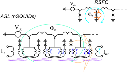
nSQUID-based circuits were successfully tested 43 at GHz clock frequency. At lower frequency, MHz, their energy dissipation per logic operation was estimated 8 to be close to the thermodynamic limit, .
Since nSQUID circuits utilize SFQ clocking, the clock rate (and hence, the power dissipation) can be adjusted “in flight” like in RSFQ circuits. Note that the energy associated with SFQ creation or annihilation is much greater than the thermodynamic limit at K. SFQs are “recycled” to avoid this energy dissipation. For this purpose the circuits are made in closed loop manner as “timing belts” 44 . Thus, total number of SFQs remains unchanged. However, this imposes certain restriction on the circuit design.
I.4 Discussion
We considered non-adiabatic and adiabatic logics which implementations are different mainly in the type of power supply, AC or DC. Each type has its own advantages and disadvantages.
The most attractive feature of AC versus DC bias is that the power is supplied in series. We should note that this feature can be utilized also for DC biased circuits by using AC-to-DC converter ACDCconv . At particular frequency of AC power source the required bias voltage can be obtained by serial connection of these converters. Power supply of different parts of large scale DC biased circuit by such voltage sources could eliminate the need for the circuit partitioning.
In general, SFQ AC biased circuits are good in design of large regular structures. The largest superconductor digital circuit is AC biased shit register containing 809 thousand Josephson junctions RQL_SR . It was used as a fabrication process benchmark circuit like a kind of “scan chain”.
DC power source is most convenient in terms of providing the power into the cryogenic system. Indeed, the bandwidth of microwave cables is often narrow to prevent hit inflow. In order to overcome the limitation on the maximum frequency of AC biased circuits it was proposed to use a DC-to-AC converter as on-chip power source DCAC . This converter was successfully tested in experiment providing oscillation frequency of GHz. The output AC bias current amplitude can be tuned by varying DC bias current of the convertor. Utilization of AC-to-DC and DC-to-AC converters allows to use circuits based on different logics on a single chip, increasing the variability of design.
Physical localization of information corresponding to quantization of magnetic flux leads to another issue, especially in digital SFQ circuits. Due to low gain from Josephson junctions, the circuits are featured by low fan-out. An SFQ has to propagate through large and slow SFQ splitter tree to split information into multiple branches. The same situation is with merging of multiple outputs.
Solution of this problem can be found in utilization of magnetic control over cells by using current control line. This approach can be realized with SFQ-to-current loop converter CLD ; RSFQdecoder . Similar technique can be used in merging of multiple outputs SQFMerg .
SFQ-to-current conversion can be realized also by Superconducting-Ferromagnetic Transistor (SFT) SFTNev or by “non-Josephson” device like n-Tron nTron1 . The former is the three (or four) terminal device comprising two stacked Josephson junctions. One of them, “injector”, (containing ferromagnetic layer(s)) serves for injection of spin-polarized electrons in common superconducting electrode of both junctions, thus suppressing its superconductivity. This manifests itself as redistribution of superconducting current flowing through this electrode or as degradation of “acceptor” (typically SIS junction) critical current depending on configuration of the device SFTNev1 . While having good input/output isolation, SFT is capable of providing voltage, current, and power amplification.
n-Tron is the three terminal device comprising superconducting strip with a narrow in the middle to which the third terminal tip is connected. Current pulse from the third terminal switch off superconductivity of the nanowire, that is similar to SFT operation to some extent. Unlike Josephson junction, the nanowire in resistive state possesses several resistance which provide high output impedance and high voltage signal nTron2 ; nTron3 . Both devices can be utilized as an interface SFTNev1 ; nTronCMOS1 ; nTronCMOSmem between superconductor circuit and CMOS electronics or memory depending on requirements to output signal and energy efficiency.
It is well known that the major computation time and power consumption is associated with communications between logic and memory circuits MAGIC2 . Logic cells possessing feature of internal memory are now being considered as possible element base for development of new, more efficient computers Mec1 ; Mec2 . Superconductor logic circuits utilizing their internal memory were named “MAGIC” (Memory And loGIC) circuits MAGIC2 ; MAGIC1 . This concept is based on conventional ERSFQ cells involving their renaming or rewiring. It promises an increase in clock rate to above 100 GHz threshold, combined with up to ten-fold gain in functional density. In general, the mentioned quantum localization of information and high non-linearity of Josephson junctions make superconductor circuits to be ideally suit for implementation of unconventional computational paradigms like cellular automata CellA1 ; CellA2 , artificial neural networks ANN1 ; ANN2 ; ANN3 or quantum computing QCR1 ; QCR2 ; QCRIF1 ; QCRIF2 ; QCRIF3 .
Unfortunately, the major problem of superconductor circuits does not relate to a particular logic of computation. Low integration density in all cases limits complexity, and therefore performance of modern digital superconductor device. Possible solutions here are miniaturization of existing element base and increase of its functionality.
The first one can be performed by scaling down the SIS Josephson junction 250nmJJ , or search for other high accuracy technological processes providing nanosized junctions with high critical current density and normal-state resistance 250nmJJ ; aSi ; aSi1 . Another direction of the research is substitution of conventional loop inductance for kinetic inductance or inductance of Josephson junction T . This also allows to make the circuits more energy efficient. Indeed, Josephson junction critical current and loop inductance are linked for SFQ circuits. Their product should be for proper operation. While the critical current has to be decreased in order to improve the energy efficiency, , this leads to increase in the inductance making the circuit to be sparse. Miniaturization of inductance weakens this problem. Unfortunately, transformer remains an inherent component of the circuits which can not be miniaturized in this way.
One should note that contrary to CMOS technology where transistor layer is implemented on a substrate, Josephson junctions can be fabricated at any layer. This provides opportunity for utilization of 3D architecture. With planned technological advances, the Josephson junction density up to cm2 seems achievable.
Finally, Josephson junctions with unconventional current-phase relation (CPR) can be utilized in a circuit for its miniaturization. For example, the so-called “”-junction (the junction with constant shift of its CPR) can be used as a “phase battery” providing constant phase shift pJJ1 ; pJJ2 instead of conventional transformer. Control of the junction CPR phase shift LUTwFJJ can provide the change in the logic cell functioning, e.g., converting AND to OR. This mechanism can be also used for implementation of memory cell LUTwFJJ ; NGmemcell .
Historically, the problem of element base miniaturization was first recognized in development of superconductor random access memory (RAM). Since that time, the need for dense cryogenic RAM is the major stimulus for innovative research in this area.
II Memory
Among the many attempts to create a cryogenic memory compatible with energy-efficient superconducting electronics, we want to single out the four most productive competing directions: (A) SQUID-based memory, (B) hybrid Josephson-CMOS memory, (C) JMRAM and (D) OST-MRAM.
II.1 SQUID-based memory
The presence or absence of SFQ(s) in a superconducting loop can be the physical basis for a digital memory element. Due to high characteristic frequency of Josephson junction, SQUID-based memory cells stand out with fast (few picoseconds) BLZ write/read time favorable for RAM which is indispensable for data processor. Throughout various SQUID-based RAM realizations memory element was provided with destructive MDRO1 ; MDRO2 ; MDRO3 or non-destructive MNDRO1 ; MNDRO2 ; MNDRO3 readout. Memory cell contained accordingly from two MDRO1 to ten BLZ Josephson junctions. With Josephson junction micron-scale dimensions in the late 1990-s this resulted in memory cell area of an order of few hundreds of microns squared. While power dissipation per write/read operations was at W level, memory chip capacity MNDRO3 was only up to kb. In the particular kb RAM memory MNDRO3 the memory drivers and sensing circuits required AC power which limited its clock frequency to MHz. Later, all-DC-powered high-speed SFQ RAM based on pipeline structure for memory cell arrays was proposed MNDRO4 . Estimation showed that this approach allows up to Mb memory on cm2 chip operated at GHz clock frequency and featuring mW power dissipation. Still, it was never realized in experiment.
II.2 Hybrid Josephson-CMOS memory
Low integration density of SQUID-based memory cells seemed to be significant obstacle to the development of low-temperature RAM with reasonable capacity. This approach was succeeded by hybrid Josephson-CMOS RAM where Josephson interface circuits were amended by CMOS memory chip HMEM1 ; HMEM2 ; HMEM3 ; HMEM4 ; HMEM5 . This combination allowed to develop kb, K temperature RAM with ps read time, and mW power dissipation for write/read operations, accordingly HMEM5 . CMOS memory cell was composed of 8 transistors. While being fabricated in a nm CMOS process, the cell size was about three orders of magnitude less than the one of its SQUID-based counterparts. Main challenge in design of this memory system was amplification of sub-mV superconductor logic signal up to the V level required by CMOS circuits. This task was accomplished in two stages. First, the signal was amplified to mV using a Suzuki stack, which can be thought as a SQUID with each Josephson junction substituted by a series array of junctions for high total resistance SuzukiS . At the second step, the reached mV signal drives high sensitive CMOS comparator to produce the volt output level.
Suzuki stack HMEM4 and CMOS comparator CMOScomp were optimized for best compromise of power and time performance. Their simulated power delay product for read operation were mW ps ( pJ) and mW ps ( pJ). This made up % and % of total memory system read power and time delay, correspondingly. These results exhibit severe restriction of overall system performance by the interface circuits. Recently, it was shown that the power consumption can be significantly decreased with utilization of energy efficient ERSFQ decoders and n-Trons as high voltage drivers nTronCMOSmem . This could provide the energy efficiency improvement up to times for kb, and up to times for Mb memory. In the latter case, the access time in a read operation is estimated to be ns.
While the hybrid memory approach showed better memory capacity, its power consumption and time requirements are still prohibitive. It was summarized that for implementation of practical low-temperature RAM one should meet the following criteria MRep : (i) scale: memory element dimension nm ( nm pitch); (ii) write operation: J energy with ps time delay per cell; (iii) read operation: J energy with ps time delay per cell. An idea to meet the requirements nowadays is to bring spintronics (including superconductor spintronics) in RAM design.
II.3 JMRAM
It is possible to reduce drastically the size of superconducting memory cell by using controllable Josephson junction with magnetic interlayers instead of SQUID JMRAM1 ; JMRAM2 ; JMRAM3 ; JMRAM4 ; JMRAM5 ; JMRAM6 . Topology of such magnetic Josephson junction (MJJ) is usually of two types: (i) sandwich topology which is well suited for CMOS-compatible fabrication technology, and (ii) the one with some heterogeneity of the junction weak-link area in-plane of the layers. Below we present MJJ valves according to this classification.
II.3.1 MJJ valve of sandwich topology
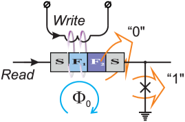
Search for an optimal way of compact MJJ valve implementation remains under way now. The most obvious solution is to use two ferromagnetic layers with different magnetic rigidity in the area of the junction weak link JMRAM7 ; JMRAM8 ; JMRAM9 . Critical current of such junction is determined by effects resulting from coexistence and competition of two orderings for electron spins: “superconducting” (S) (with usually antiparallel spins of electrons in the so-called “Cooper pairs”) and “ferromagnetic” (F) (with parallel ordering of electron spins). Magnetization reversal of “weak” F-layer leads to switching between collinear and anti-collinear orientations of the F-layers magnetic moments in the bilayer. This, in turn, provides alteration in the total effective exchange energy, , and hence, in MJJ critical current effective suppression. While magnetization reversal can be executed by application of an external magnetic field JMRAM10 , the critical current can be read-out, e.g., with MJJ inclusion into decision making pair JMRAMRyaz , see Figure 14. It is possible to trace some analogy between this effect and the phenomenon of giant magnetoresistance JMRAM12 which is actively used in conventional magnetic memory cells.
A common drawback of most MJJs is small value of their characteristic frequency () in comparison with SIS junction. Indeed, here one has to perform the magnetization reversal of weak F-layer with relatively small exchange energy in order to manipulate the total critical current against the background of its considerable suppression by the strong ferromagnet. Low outflows in slow read operation and complicates MJJ integration in SFQ logic circuits.
There are several approaches to solve this problem. One of them is the using of noncollinearly magnetized ferromagnetic layers JMRAM13 ; JMRAM14 ; JMRAM15 ; conclmem1 . In this case, the triplet superconducting correlations of electrons are formed in the junction weak-link area. A part of them are featured by collinear orientation of electron spins in Cooper pairs. They are unaffected by exchange field of the ferromagnets, thus increasing MJJ critical current while maintaining its normal state resistance. The “triplet” current can be controlled by external magnetic field through magnetization reversal Birgereq . Still, this approach implies implementation of a number of additional layers (and interfaces) in the structure that reduces its critical current.
One should also note that alteration could result in shift of MJJ CPR. In this case the valve can be utilized as controllable phase battery LUTwFJJ . Inclusion of such MJJ into SQUID loop allows fast read-out of its state NGmemcell . However, here miniaturization reduces only to replacement of the SQUID inductance by the MJJ.
Another approach is based on localization of magnetic field source outside Josephson junction weak-link area but in the nearest proximity FFoutJJ1 ; FFoutJJ2 ; FFoutJJ3 ; FFoutJJ4 . For example, F-bilayer can be placed on top of SIS junction. In this case, stray magnetic field penetrating into the junction area controls its critical current. If the junction S-layer neighboring the F-bilayer is thin enough, the coupling of the vector potential of the stray magnetic field to superconducting order parameter phase could also noticeably affect Josephson phase difference across SIS junction. SIS junction is utilized here just for read-out the ferromagnet state, and therefore, its characteristic frequency remains high. Still, since the strength of magnetic field is proportional to the ferromagnet volume, a possibility of miniaturization of such memory element is doubtful.
Critical current modulation can be obtained even in the structure with a single magnetic layer by changing the value of its residual magnetization JMRAM16 . It is also possible to improve the characteristic frequency by the inclusion of dielectric (I) and thin superconducting (s) layers in MJJ weak-link area to increase and , correspondingly JMRAM19 ; JMRAM20 ; JMRAM21 ; JMRAM22 ; JMRAM23 ; JMRAM24 ; JMRAM25 ; JMRAM26 . Such SIsFS valves possess characteristics close to SIS junction JMRAM21 . However, compatibility with superconductors requires utilization of ferromagnets with relatively low coercive field, which are typically characterized by non-square shape of the hysteresis loop. This in turn outflows into uncertainty of MJJ critical current at zero applied magnetic field after multiple magnetization reversals. In addition, miniaturization here faces the same difficulties as in the previous approach. For these reasons, it seems especially fruitful to replace the I and F layers with two magnetic insulator IF-layers to construct a Josephson S(IF)s(IF)S valve JMRAM27 ; JMRAM28 ; JMRAM29 . Its operation relies on variable suppression of superconductivity of the middle s-layer. Yet, this promising structure is complicated for fabrication.
II.3.2 MJJ valve with in-plane heterogeneity of the weak-link area
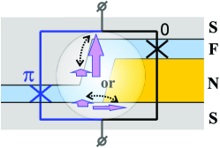
The second type of valves implies heterogeneity of the weak-link region in the junction plane providing separation of the structure into two parts. CPR of these parts can be different, e.g., the conventional CPR and the ones shifted in phase by JMRAM24 ; JMRAM18 . Such MJJ may be thought as nanoSQUID with conventional and “” lumped junctions. Its implementation may comprise a ferromagnetic interlayer and a sandwich containing the same F-layer and a normal metal (N) layer, see Figure 15. If F-layer magnetization is aligned perpendicular to the nanoSQUID plane, it compensates the Josephson phase gradient across the MJJ making its critical current to be high. While the magnetization is being rotated at , this effect is turned off and becomes low. Here for proper operation of this SF-NFS-based MJJ the flux of residual magnetization must be comparable with the flux quantum .
The second common problem of MJJ-based memory is a long time of write operation. Bit write is commonly performed by magnetization reversal of at least one of F-layers. For this reason, recording time is of an order of inverse frequency of ferromagnetic resonance. It is usually more than two orders of magnitude larger than the characteristic time of SIS junction switching. Thus, elimination of magnetization reversal from the valves operation is desired. It is worth noting that nano-sized trap for single Abrikosov vortex in the vicinity of Josephson junction JMRAM33 ; JMRAM34 allows to realize fast enough write operation. However, energy dissipation associated with annihilation of such vortex ( J) may contradict with the paradigm of energy-efficiency.
This challenge can be met with MJJ having bistable Josephson potential energy. Josephson phases of its ground states could be equal to (). One can realize both write and read operations with such -junction on picosecond timescale JMRAM35 ; JMRAM36 ; JMRAM37 ; JMRAM38 ; JMRAM381 ; JMRAM39 ; JMRAM40 . The disadvantage of this approach is the difficulties with -state implementation. In practice, it is possible only in the structure with heterogeneous weak-link region of a rather large size.
One more operation principle of MJJ valves relies on control of superconducting phase domains formation JMRAM26 . The effect can be realized in SIsFS MJJ with sFS part substituted, e.g., for heterogeneous SF-NFS combination. The middle s-layer is broken on domains with different superconducting phases if Josephson phases of the structure parts are different, and vice versa. This process can be controlled by current injection through sFS or sFNS parts. The domain formation significantly changes the MJJ critical current. This MJJ provides fast read and write operations with no need for application of external magnetic field. Still, fabrication of compact Josephson junctions having the inhomogeneous weak-link region with reproducible characteristics is a difficult technological task.
II.4 OST-MRAM
The next considered type of cryogenic memory is the hybrid approach combining superconducting control circuits with spintronics memory devices. Here due to spin-based interactions between atoms in the crystal lattice and electrons, orientations of ferromagnets magnetization can determine the amount of current flow. And vice versa, spin-polarized current can affect orientations of the magnetizations. The last effect is the so-called “spin transfer torque” (STT). It was suggested as a control mechanism for magnetic memory COST1 ; COST2 ; COST3 . However, high speed and low energy of write operation can not be provided with conventional spin-valve topology with collinear orientations of ferromagnets magnetizations COST4 .
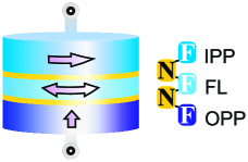
Orthogonal spin transfer (OST) device allows to overcome the difficulties. This structure consists of an out-of-plane ferromagnetic polarizer (OPP), a free F-layer (FL), and a fixed F in-plane polarizer/analyzer (IPP), see Figure 16. “Write” current pulse passing through OPP provides STT effect in FL which acts to lift its magnetization out of plane. Magnetization is then rotated about the out-of-plane axis, according to Landau-Lifshitz-Gilbert equation. Current pulse applied to IPP read-out collinear or anti-collinear magnetizations of in-plane magnetized F-layers.
It is possible to obtain the necessary magnetization reversal with correct selection of the write pulse amplitude and duration. Quasi-static and dynamic switching characteristics of OST devices have been analyzed at cryogenic temperatures: switching between parallel and anti-parallel spin-valve states has been demonstrated for mA current pulses of sub-ns duration COST4 ; COST5 ; COST6 .
Clear advantages of the considered approach is elimination of control lines for magnetic field application, and implementation of fast magnetization reversal at sub-ns timescale. At the same time, the problems like relatively low percent of magnetoresistance, and the ones associated with possible magnetization over-rotation still prevent its practical application. The latter one can be overcome to some extend by involving both IPP and OPP polarizers into FL switching process COST4 .
One could note that application of STT effect in some of MJJ valves is of considerable interest. STT in voltage biased superconducting magnetic nanopillars (SFNFS and SFSFS junctions) has been studied for both equilibrium and nonequilibrium cases COST9 ; COST10 ; COST11 ; COST12 ; COST13 . However, rich dynamics resulting from interplay of multiple Andreev reflection, spin mixing, spin filtering, spectral dynamics of the interface states, and the Josephson phase dynamics requires further research for evaluation of STT application appropriateness in superconducting memory structures.
II.5 Discussion
Lack of suitable cryogenic RAM is “… the main obstacle to the realization of high performance computer systems and signal processors based on superconducting electronics.” MEMDIS1 While JMRAM and OST-MRAM look as the most advanced approaches, they still require further improvement in a number of critically important areas.
Progress in considered variety of device types with no clear winner is impossible without researches on new magnetic materials like PdFe, NiFe(Nb,Cu,Mo), Co/Ru/Co, [Co/Ni]n etc., and novel magnetization reversal mechanisms MEMDIS2 ; MEMDIS3 ; MEMDIS4 . They can lead to development of new operation principles combining superconductivity and spintronics.
Inverse proximity effect at SF boundaries dictates utilization of pretty thin (at nm scale) magnetic layers. However, characteristics of memory devices typically depends exponentially on the F-layers thicknesses and significantly affected by interfacial roughness. This challenge can be met with further development of high-accuracy thin-film technological processes in modern fabrication technology.
Substantial part of circuit area, time delay and dissipated power in memory matrix is more likely to be associated with address lines rather than with memory cells. This makes optimization of intra-matrix interconnections and memory cell architecture of significant importance.
While we considered here only the most developed solutions for superconducting valves and memory elements, there are many other approaches to create nanosized controllable superconducting devices for applications in memory and logic. We can point out on our discretion: the nanoscale superconducting memory based on the kinetic inductance MEMDIS5 , and the superconducting quantum interference proximity transistor MEMDIS6 . Such concepts could bring novel idea into nanoscale design of superconducting circuits.
Conclusion
In conclusion, we discussed different superconductor logics providing fast ( GHz) and energy efficient ( J per bit) operation of circuits in non-adiabatic and adiabatic regimes. The last one allows implementation of the most energy efficient physically and logically reversible computations with no limit for minimum energy dissipation per logic operation. Possibilities to combine the schemes based on different logics as well as utilization of different (e.g. superconductor and semiconductor) technologies in a single device design are presented.
Considered physical principles underlying superconducting circuits operation provide possibility for development of devices based on unconventional computational paradigms. This could be the basis for a cryogenic cross-platform supercomputer, where each task can be executed in the most effective way. In our opinion, the development of superconducting circuits performing non-classical computations like cellular automata, artificial neural networks, adiabatic, reversible, and quantum computing is indispensable to get all the benefits of the superconductor technology.
Low integration density, and hence low functional complexity of the devices, is identified as the major problem of the considered technology. This issue can be addressed with further miniaturization of basic elements and modernization of cell libraries, including introduction of novel devices like the ones based on nanowires or magnetic Josephson junctions.
The problem of low integration density is especially acute in RAM design. We considered here four different approaches to cryogenic RAM development with no clear winner. Progress in this area now implies elaboration of new operation principles based on synergy of different physical phenomena like superconductivity and magnetism, and appearance of novel effects, as for example, triplet spin valve memory effect conclmem1 or superconducting control of the magnetic state JMRAM27 . Proposed concepts of new controllable devices could eventually change the face of superconductor technology making it universal platform of future high-performance computing.
Acknowledgements.
The authors are grateful to Alexander Kirichenko and Timur Filippov for fruitful discussions. This work was supported by grant No. 17-12-01079 of the Russian Science Foundation, Anatoli Sidorenko would like to thank the support of the project of the Moldova Republic National Program Nonuniform superconductivity as the base for superconducting spintronics ( SUPERSPIN , 2015-2018), partial support of the Program of Competitive Growth at Kazan Federal University is also acknowledged.References
- (1) “Intel Puts the Brakes on Moore’s Law” by Tom Simonite at MIT Tech. Review, 23 March 2016. https://www.technologyreview.com/s/601102/intel-puts-the-brakes-on-moores-law/ (accessed June 02, 2017).
- (2) “Moore’s Law Is Dead. Now What?” by Tom Simonite at MIT Tech. Review, 13 May 2016. https://www.technologyreview.com/s/601441/moores-law-is-dead-now-what/ (accessed June 02, 2017).
- (3) “The Chip Design Game at the End of Moore’s Law” by Robert Colwell at ”Hot Chips”, August 2013. http://www.hotchips.org/wp-content/uploads/hc_archives/hc25/HC25.15-keynote1-Chipdesign-epub/HC25.26.190-Keynote1-ChipDesignGame-Colwell-DARPA.pdf (accessed June 02, 2017).
- (4) Ball P. Nature 2012, 492, 174-176.
- (5) Service, R. F. Science 2012, 335, 394-396.
- (6) Markov, I. L. Nature 2014, 512, 147-154.
- (7) “Sunway TaihuLight”. http://www.top500.org/system/178764 (accessed June 02, 2017).
- (8) Brock, D.C. IEEE Spectr. 2016, 53, 54-60.
- (9) “SciDAC Review, 2010” by Geist, A. http://www.scidacreview.org (accessed June 02, 2017).
- (10) “Beyond Moore’s Law and Implications for Computing in Space” by Air Force Research Laboratory presentation, July 2, 2015. https://www.osti.gov/scitech/servlets/purl/1260528 (accessed June 02, 2017).
- (11) Mukhanov, O. A. IEEE Trans. Appl. Supercond. 2011, 21, 760-769.
- (12) Zhirnov, V. V.; Cavin, R. K.; Hutchby, J. A.; Bourianoff G. I. Proc. IEEE 2003, 91, 1934-1939 .
- (13) Xu, Q.; Yamanashi, Y.; Ayala, C. L.; Takeuchi, N.; Ortlepp, T.; Yoshikawa, N. Design of an Extremely Energy-Efficient Hardware Algorithm Using Adiabatic Superconductor Logic. In Proceedings of 15th International Superconductive Electronics Conference, ISEC’2015, Nagoya, Japan, July 6-9, 2015; pp DS-P21.
- (14) “Cryogenic Computing Complexity (C3)”. https://www.iarpa.gov/index.php/research-programs/c3 (accessed June 02, 2017).
- (15) Holmes, D. S.; Kadin, A. M.; Johnson, M. W. Computer 2015, 48, 34-42.
- (16) Likharev, K.; Semenov, V. IEEE Trans. Appl. Supercond. 1991, 1, 3-28.
- (17) Likharev, K. K.; Mukhanov, O. A.; Semenov, V. K. SQUID’85 1985, 1103-1108.
- (18) Ginzburg, V. L.; Landau L. D. J. Exp. Theor. Phys. 1950, 20, 1064-1081.
- (19) Stewart, W. C. Appl. Phys. Lett. 1968, 12, 277.
- (20) Tolpygo, S. K. Low. Temp. Phys. 2016, 42, 463-485.
- (21) “NIOBIUM PROCESS”. http://www.hypres.com/foundry/niobium-process/ (accessed June 02, 2017).
- (22) Gupta, D.; Li, W.; Kaplan, S.B.; Vernik, I.V. IEEE Trans. Appl. Supercond. 2001, 11, 731-734.
- (23) Filippov, T. V.; Amparo, D.; Kamkar, M. Y.; Walter, J.; Kirichenko, A. F.; Mukhanov, O. A.; Vernik, I. V. Experimental Investigation of ERSFQ Circuit for Parallel Multibit Data Transmission. In Proceedings of 16th International Superconductive Electronics Conference, ISEC’2017, Sorrento, Italy, June 12-16, 2017; pp. TU-C-DIG-01.
- (24) Likharev, K. K. Phys. C Supercond. Its Appl. 2012, 482, 6-18.
- (25) Mukhanov, O. A. History of Superconductor Analog-to-Digital Converters. In 100 Years of Superconductivity; Rogalla, H.; Kes, P. Eds.; Taylor Francis: London, UK, 2011; pp 440-458.
- (26) Mukhanov, O. A.; Gupta, D; Kadin, A. M.; Semenov, V. K. Proc. IEEE, 2004, 92, 1564-1584.
- (27) Mukhanov, O. A. Digital Processing, Superconductor Digital Electronics. In Applied Superconductivity: Handbook on Devices and Applications; Seidel, P., Ed., Wiley-VCH Verlag GmbH Co. KGaA: Weinheim, Germany, 2015; 1-28.
- (28) Chen, W.; Rylyakov, A.V.; Patel, V.; Lukens, J.E.; Likharev, K.K. Appl. Phys. Lett. 1998, 73, 2817-2819.
- (29) Hamilton, C. A.; Lloyd, F. L. IEEE Electron. Dev. Lett. 1982, 3, 335-338.
- (30) Mukhanov, O. A.; Semenov, V. K.; Likharev, K. K. IEEE Trans. Magn. 1987, MAG-23, 759-762.
- (31) Rylyakov, A. IEEE Trans. Appl. Supercond. 1997, 7, 2709-2712.
- (32) Yoshikawa, N.; Kato, Y. Supercond. Sci. Technol. 1999, 12, 918-920.
- (33) Yamanashi, Y.; Nishigai, T.; Yoshikawa, N. IEEE Trans. Appl. Supercond. 2007, 17, 150-153.
- (34) Tanaka, M.; Kitayama, A.; Kouketsu, T.; Ito, M.; Fujimaki, A. Japan J. Appl. Phys. 2012, 51, 053102.
- (35) Tanaka, M.; Kitayama, A.; Kouketsu, T.; Ito, M.; Fujimaki, A. IEEE Trans. Appl. Supercond. 2013, 23, 1701104.
- (36) Rylyakov, A. V.; Likharev, K. K. IEEE Trans. Appl. Supercond. 1999, 9, 3539-3544.
- (37) Kirichenko, D. E.; Sarwana, S.; Kirichenko, A. F. IEEE Trans. Appl. Supercond. 2011, 21, 776-779.
- (38) Volkmann, M. H.; Sahu, A.; Fourie, C. J.; Mukhanov, O. A. Supercond. Sci. Technol. 2013, 26, 015002.
- (39) Volkmann, M. H.; Vernik, I. V.; Mukhanov, O. A. IEEE Trans. Appl. Supercond. 2015, 25, 1301005.
- (40) Vernik, I. V.; Kaplan, S. B.; Volkmann, M. H.; Dotsenko, A. V.; Fourie, C. J.; Mukhanov, O. A. Supercond. Sci. Technol. 2014, 27, 044030.
- (41) Mukhanov, O. A. IEEE Trans. Appl. Supercond. 1993, 3, 3102-3113.
- (42) Averin, D. V.; Rabenstein, K.; Semenov, V. K. Phys. Rev. B 2006, 73, 094504.
- (43) Soloviev, I. I.; Klenov, N. V.; Pankratov, A. L.; Il’ichev, E.; Kuzmin, L. S. Phys. Rev. E 2013, 87, 060901(R).
- (44) Filippov, T. V.; Sahu, A; Sarwana, S; Gupta, D; Semenov, V. K. IEEE Trans. Appl. Supercond. 2009, 19, 580-584.
- (45) Peng, X.; Xu, Q.; Kato, T.; Yamanashi, Y.; Yoshikawa, N.; Fujimaki, A.; Takagi, N.; Takagi, K.; Hidaka, M. IEEE Trans. Appl. Supercond. 2015, 25, 1301106.
- (46) Herr, Q. P.; Herr, A. Y.; Oberg, O. T.; Ioannedis, A.G. J. Appl. Phys. 2011, 109, 103903.
- (47) Oberg, O. T. Ph.D Thesis, Graduate School of the University of Maryland 2011.
- (48) Herr, A. Yu.; Herr, Q. P.; Oberg, O. T.; Naaman, O.; Przybysz J. X.; Borodulin, P.; Shauck, S. B. J. Appl. Phys. 2013, 113, 033911.
- (49) Landauer, R. IBM J. Res. Dev. 1961, 5, 183-191.
- (50) Takeuchi, N.; Yamanashi, Y.; Yoshikawa, Sci. Rep. 2014, 4, 6354.
- (51) Likharev K. K. IEEE Trans. Magn. 1976, 13, 242-244.
- (52) Goto, E. Proc. IRE 1959, 47, 1304-1316.
- (53) Likharev, K. K.; Korotkov, A. N. Science 1996, 273, 763-765.
- (54) Lent, C. S.; Tougaw, P. D. Proc. IEEE 85 1997, 541-557.
- (55) Likharev, K.K. Int. J. Theor. Phys. 1982, 21, 311-326.
- (56) Likharev, K. K.; Rylov, S. V.; Semenov V. K. IEEE Trans. Magn. 1985, MAG-21, 947-950.
- (57) Hosoya, M.; Hioe, W.; Casas, J.; Kamukawai, R.; Harada, Y.; Wada, Y.; Nakane, H.; Suda, R.; Goto, E. IEEE Trans. Appl. Supercond. 1991, 1, 77-89.
- (58) Bennett, C. H. IBM Journ. Res. Dev. 1973, 17, 525-532.
- (59) Hosoya, M.; Hioe, W.; Takagi, K.; Goto, E. IEEE Trans. Appl. Supercond. 1995, 5, 2831 - 2834.
- (60) Johnson, M. W.; Bunyk, P.; Maibaum, F.; Tolkacheva, E.; Berkley, A. J.; Chapple, E. M.; Harris, R.; Johansson, J.; Lanting, T.; Perminov, I.; Ladizinsky, E.; Oh, T.; Ros, G. Supercond. Sci. Technol. 2010, 23, 065004.
- (61) Berkley, A. J.; Johnson, M. W.; Bunyk, P.; Harris, R.; Johansson, J.; Lanting, T.; Ladizinsky, E.; Tolkacheva, E.; Amin, M. H. S.; Rose, G. Supercond. Sci. Technol. 2010, 23, 105014.
- (62) “Fujimaki Laboratory” 2014-2015. http://www.super.nuqe.nagoya-u.ac.jp/alca/ (accessed June 02, 2017).
- (63) Takeuchi, N.; Ozawa, D.; Yamanashi, Y.; Yoshikawa, N. Supercond. Sci. Technol. 2013, 26, 035010.
- (64) Takeuchi, N.; Yamanashi, Y.; Yoshikawa, N. Appl. Phys. Lett. 2013, 102, 052602.
- (65) Takeuchi, N.; Yamanashi, Y.; Yoshikawa, N. Appl. Phys. Lett. 2013, 103, 062602.
- (66) Takeuchi, N.; Ortlepp, T.; Yamanashi, Y.; Yoshikawa, N. J. Appl. Phys. 2014, 115, 103910.
- (67) Takeuchi, N.; Yamanashi, Y.; Yoshikawa, N. J. Appl. Phys. 2015, 117, 173912.
- (68) Takeuchi, N.; Yamanashi, Y.; Yoshikawa, N. Supercond. Sci. Technol. 2015, 28, 015003.
- (69) Nagasawa, S.; Hinode, K.; Satoh, T.; Akaike, H.; Kitagawa, Y.; Hidaka, M. Phys. C Supercond. Its Appl. 2004, 412, 1429-1436.
- (70) Narama, T.; Yamanashi, Y.; Takeuchi, N.; Ortlepp, T.; Yoshikawa, N. Demonstration of 10k Gate-Scale Adiabatic-Quantum-Flux-Parametron Circuits. In Proceedings of 15th International Superconductive Electronics Conference, ISEC’2015, Nagoya, Japan, July 6-9, 2015; pp DS-P04-INV .
- (71) Fang, K; Takeuchi, N.; Ando, T; Yamanashi, Y.; Yoshikawa, N. J. Appl. Phys. 2017, 121, 143901.
- (72) Semenov, V. K.; Danilov, G. V.; Averin, D. V. IEEE Trans. Appl. Supercond. 2003, 13, 938 - 943.
- (73) Semenov, V. K.; Danilov, G. V.; Averin, D. V. IEEE Trans. Appl. Supercond. 2007, 17, 455 - 461.
- (74) Ren, J.; Semenov, V. K.; Polyakov, Y.A.; Averin, D.V.; Tsai, J.S. IEEE Trans. Appl. Supercond. 2009, 19, 961- 967.
- (75) Ren, J.; Semenov, V. K. IEEE Trans. Appl. Supercond. 2011, 21, 780-786.
- (76) Averin, D. V.; Deng, Q. J. Exp. Theor. Phys. 2014, 119, 1152-1162.
- (77) Semenov, V. K.; Polyakov, Y. A.; Tolpygo, S. K. IEEE Trans. Appl. Supercond. 2015, 25, 1301507.
- (78) Semenov, V. K.; Polyakov, Y. A.; Tolpygo, S. K. IEEE Trans. Appl. Supercond. 2017, 27, 1301409.
- (79) Takeuchi, N.; Yamanashi, Y.; Yoshikawa, N. Supercond. Sci. Technol. 2013, 26, 035018.
- (80) Nagasawa, S.; Hinode, K.; Stoh, T.; Kitagawa, Y.; Hidaka, M. Supercond. Sci. Technol. 2006, 19, 325-330.
- (81) Kirichenko, A. F.; Vernik, I. V.; Mukhanov, O. A.; Ohki, T. A. IEEE Trans. Appl. Supercond. 2015, 25, 1301304.
- (82) Sato, K.; Yamanashi, Y.; Yoshikawa, N. IEEE Trans. Appl. Supercond. 2015, 25, 1301605.
- (83) Nevirkovets, I. P.; Chernyashevskyy, O.; Prokopenko, G. V.; Mukhanov, O. A., Ketterson, J. B. IEEE Trans. Appl. Supercond. 2014, 24, 1800506.
- (84) McCaughan, A. N.; Berggren, K. K. Nano Lett. 2014, 14, 5748-5753.
- (85) Nevirkovets, I. P.; Chernyashevskyy, O.; Prokopenko, G. V.; Mukhanov, O. A., Ketterson, J. B. IEEE Trans. Appl. Supercond. 2015, 25, 1800705.
- (86) Kerman, A. J.; Yang, J. K. W.; Molnar, R. J.; Dauler, E. A.; Berggren, K. K. Phys. Rev. B 2009, 79, 100509.
- (87) Semenov, A. D.; Gol’tsman, G. N.; Sobolewski, R. Supercond. Sci. Technol. 2002, 15, R1-16.
- (88) Zhao, Q. -Y.; McCaughan, A. N.; Dane, A. E.; Berggren, K. K.; Ortlepp, T. Supercond. Sci. Technol. 2017, 30, 044002.
- (89) Tanaka, M.; Suzuki, M.; Konno, G.; Ito, Y.; Fujimaki, A.; Yoshikawa, N. IEEE Trans. Appl. Supercond. 2017, 27, 1800904.
- (90) Semenov, V.K. Erasing Logic-Memory Boundaries in Superconductor Electronics. In IEEE International Conference on Rebooting Computing (ICRC), 2016 IEEE ICRC, San Diego, CA, USA, October 17 - 19, 2016; pp 16463827.
- (91) Di Ventra, M.; Pershin, Y.V. Nat. Phys. 2013, 9, 200.
- (92) Yang, J.J.; Strukhov, D.B.; Stewart, D.R. Nat. Nanotechnol. 2012, 8, 13.
- (93) Semenov, V.K. IEEE Trans. Appl. Supercond. 2013, 23, 1700908.
- (94) Olson Reichhardt, C.J.; Reichhardt, C.; Hastings, M.B.; Janko, B. Phys. C Supercond. 2004, 404, 266-272.
- (95) Milosevic, M.V.; Berdiyorov, G.R.; Peeters, F.M. Appl. Phys. Lett. 2007, 91, 212501.
- (96) Crotty, P.; Schult, D.; Segall, K. Phys. Rev. E 2010, 82, 011914.
- (97) Chiarello, F.; Carelli, P.; Castellano, M.G.; Torrioli, G. Supercond. Sci. Technol. 2013, 26, 125009.
- (98) Schegolev, A. E.; Klenov, N. V.; Soloviev, I. I.; Tereshonok, M. V. Beilstein J. Nanotechnol. 2016, 7, 1397-1403.
- (99) Steffen, M.; DiVincenzo, D. P.; Chow, J. M.; Theis, T. N.; Ketchen, M. B. IBM J. Res. Dev. 2011, 55, 13.
- (100) Devoret, M. H.; Schoelkopf, R. J. Science 2013, 339, 1169-1174.
- (101) McDermott, R.; Vavilov, M. G. Phys. Rev. Applied, 2014, 2, 014007.
- (102) Soloviev, I. I.; Klenov, N. V.; Bakurskiy, S. V.; Pankratov, A. L.; Kuzmin, L. S. Appl. Phys. Lett. 2014, 105, 202602.
- (103) Soloviev, I. I.; Klenov, N. V.; Pankratov, A. L.; Revin, L. S.; Il’ichev, E.; Kuzmin, L. S. Phys. Rev. B 2015, 92, 014516.
- (104) Tolpygo, S. K. arXiv 2017, 1704.07683v1.
- (105) Gudkov, A. L.; Kupriyanov, M. Y.; Samus’, A. N. J. Exp. Theor. Phys. 2012, 114, 818-829.
- (106) Olaya, D.; Dresselhaus, P. D.; Hopkins, P. F.; Benz, S. P. Fabrication of High-Speed and High-Density Single-Flux-Quantum Circuits at NIST. In Proceedings of 16th International Superconductive Electronics Conference, ISEC’2017, Sorrento, Italy, June 12-16, 2017; pp. TU-MAF-08.
- (107) Ortlepp, T.; Ariando; Mielke, O.; Verwijs, C. J. M.; Foo, K. F. K.; Rogalla, H.; Uhlmann, F. H.; Hilgenkamp, H. Science 2006, 312, 1495-1497.
- (108) Feofanov, A. K.; Oboznov, V. A.; Bol’ginov, V. V.; Lisenfeld, J.; Poletto, S.; Ryazanov, V. V.; Rossolenko, A. N.; Khabipov, M.; Balashov, D.; Zorin, A. B.; Dmitriev, P. N.; Koshelets, V. P.; Ustinov, A. V. Nat. Phys. 2010, 6, 593-597.
- (109) Gingrich, E. C.; Niedzielski, B. M.; Glick, J. A.; Wang, Y.; Miller, D. L.; Loloee, R.; Pratt, W. P. Jr; Birge, N. O. Nat. Phys. 2016, 12, 564-567.
- (110) Herr, A. Y.; Herr, Q. P.; Naaman, O. Phase hysteretic magnetic Josephson junction memory cell. US 9208861 B2, December 8, 2015.
- (111) Bunyk, P.; Likharev, K.; Zinoviev, D. Int. J. High Speed Electron. Syst. 2001, 11, 257-305.
- (112) Kurosawa, I.; Nakagawa, H., Kosaka, S.; Aoyagi, M.; Takada, S. IEEE J. Solid-State Circuits 1989, 24, 1034-1040.
- (113) Suzuki, H.; Fujimaki, N.; Tamura, H. IEEE Trans. Magn. 1989, 25, 783-788.
- (114) Polonsky, S. V.; Kirichenko, A. F.; Semenov, V. K.; Likharev, K. K. IEEE Trans. Appl. Supercond. 1995, 5, 3000-3005.
- (115) Tahara, S.; Ishida, I.; Nagasawa, S.; Hidaka, M.; Tsuge, H.; Wada, Y. IEEE Trans. Magn. 1991, 27, 2626-2632.
- (116) Nagasawa, S.; Hashimoto, Y.; Numata, H.; Tahara, S. IEEE Trans. Appl. Supercond. 1995, 5, 2447-2452.
- (117) Nagasawa, S.; Numata, H.; Hashimoto, Y.; Tahara, S. IEEE Trans. Appl. Supercond. 1999, 9, 3708-3713.
- (118) Nagasawa, S.; Hinode, K.; Satoh, T.; Kitagawa, Y.; Hidaka, M. Supercond. Sci. Technol. 2006, 19, S325-S330.
- (119) Liu, Q.; Van Duzer, T.; Meng, X.; Whiteley, S. R.; Fujiwara, K.; Tomida, T.; Tokuda, K.; Yoshikawa, N. IEEE Trans. Appl. Supercond. 2005, 15, 415-418.
- (120) Yoshikawa, N.; Tomida, T.; Tokuda, K.; Liu, Q.; Meng, X.; Whiteley, S. R.; Van Duzer, T. IEEE Trans. Appl. Supercond. 2005, 15, 267-271.
- (121) Fujiwara, K.; Liu, Q.; Van Duzer, T.; Meng, X.; Yoshikawa, N. IEEE Trans. Appl. Supercond. 2010, 20, 14-19.
- (122) Ortlepp, T.; Zheng, L.; Whiteley, S. R.; Van Duzer, T. Supercond. Sci. Technol. 2013, 26, 035007.
- (123) Van Duzer, T.; Zheng, L.; Whiteley, S. R.; Kim, H.; Kim, J.; Meng, X.; Ortlepp, T. IEEE Trans. Appl. Supercond. 2013, 23, 1700504.
- (124) Suzuki, H.; Inoue, A.; Imamura, T.; Hasuo, S. IEDM Tech. Dig. 1988, 290-293.
- (125) Kong, L.; Lu, Y.; Alon, E. A multi-GHz area-efficient comparator with dynamic offset cancellation. In Custom Integrated Circuits Conference (CICC), 2011, San Jose, CA, USA, Sep. 19-21, 2011; pp 1-4.
- (126) Mukhanov, O. A. Recent Progress in Digital Superconducting Electronics. In Proceedings of 15th International Superconductive Electronics Conference, ISEC’2015, Nagoya, Japan, July 6-9, 2015; pp CRP54.
- (127) Golubov, A. A.; Kupriyanov, M. Yu.; Il’ichev E. Rev. Mod. Phys. 2004, 76, 411.
- (128) Bergeret, F. S.; Volkov, A. F.; Efetov, K. B. Rev. Mod. Phys. 2005, 77, 1321.
- (129) Blamire, M. G.; Robinson, J. W. A. Journ. Phys. Cond. Mat. 2014, 26, 453201.
- (130) Eschrig, M. Rep. Prog. Phys. 2015, 78, 104501.
- (131) Linder, J.; Robinson, J. W. A. Nat. Phys. 2015, 11, 307.
- (132) Lu, J. W.; Chen, E. Kabir, M.; Stan, M. R.; Wolf S. A. Int. Mat. Rev. 2016, 61, 456.
- (133) Bell, C.; Burnell, G.; Leung, C. W.; Tarte, E. J.; Kang, D. -J.; Blamire, M. G. Appl. Phys. Lett. 2004, 84, 1153.
- (134) Baek, B.; Rippard, W. H.; Benz, S. P.; Russek, S. E.; Dresselhaus, P. D. Nat. Commun. 2014, 5, 3888.
- (135) Qader, M. A. E.; Singh, R. K.; Galvin, S. N.; Yu, L.; Rowell, J. M.; Newman, N. Appl. Phys. Lett. 2014, 104, 022602.
- (136) Baek, B.; Rippard, W. H.; Pufall, M. R.; Benz, S. P.; Russek, S. E.; Rogalla, H.; Dresselhaus, P. D. Phys. Rev. Applied 2015, 3, 011001.
- (137) Ryazanov, V. V.; Bol’ginov, V. V.; Sobanin, D. S.; Vernik, I. V.; Tolpygo, S. K.; Kadin, A. M.; Mukhanov, O. A. Phys. Procedia 2012, 36, 35-41.
- (138) Baibich, M. N.; Broto, J. M.; Fert, A.; Nguyen Van Dau, F.; Petroff, F.; Etienne, P.; Creuzet, G.; Friederich, A.; Chazelas, J. Phys. Rev. Lett. 1988, 61, 2472.
- (139) Bergeret, F. S.; Volkov, A. F.; Efetov, K. B. Phys. Rev. Lett. 2001, 86, 3140.
- (140) Houzet, M.; Buzdin, A. I. Phys. Rev. B 2007, 76, 060504 R.
- (141) Niedzielski, B. M.; Diesch, S. G.; Gingrich, E. C.; Wang, Y.; Loloee, R.; Pratt Jr., W. P.; Birge, N. O. IEEE Trans. Appl. Supercond. 2014, 24, 1800307.
- (142) Zdravkov V. I.; Lenk D.; Morari R.; Ullrich A.; Obermeier G.; Mueller C.; Krug von Nidda H.-A.; Sidorenko A. S.; Horn S.; Tidecks R.; Tagirov L. R. Appl. Phys. Lett. 2013, 103, 062604.
- (143) Martinez, W. M.; Pratt, W. P. Jr; Birge N. O. Phys. Rev. Lett. 2016, 116, 077001.
- (144) Clinton, T. W.; Johnson, M. Appl. Phys. Lett. 2000, 76, 2116.
- (145) Samokhvalov, A. V. Phys. Rev. B 2006, 80, 134513.
- (146) Nevirkovets, I. P.; Shafraniuk, S. E.; Chernyashevskyy, O.; Yohannes, D. T.; Mukhanov, O. A.; Ketterson J. B. IEEE Trans. Appl. Supercond. 2016, 26, 1301907.
- (147) Nevirkovets, I. P.; Mukhanov, O. A. Possible use of a multi-terminal superconducting-ferromagnetic device as a memory cell. In Proceedings of 16th International Superconductive Electronics Conference, ISEC’2017, Sorrento, Italy, June 12-16, 2017; pp. TU-SDM-06.
- (148) Bol’ginov, V. V.; Stolyarov, V. S.; Sobanin, D. S.; Karpovich, A. L.; Ryazanov, V. V. J. Exp. Theor. Phys. Lett. 2012, 95, 366-371.
- (149) Larkin, T. I.; Bol’ginov, V. V.; Stolyarov, V. S.; Ryazanov, V. V.; Vernik, I. V.; Tolpygo, S. K.; Mukhanov, O. A. Appl. Phys. Lett. 2012, 100, 222601.
- (150) Golovchanskiy, I. A.; Bol’Ginov, V.V.; Stolyarov, V. S.; Abramov, N. N.; Ben Hamida, A.; Emelyanova, O. V.; Stolyarov, B. S.; Kupriyanov, M. Y.; Golubov, A. A.; Ryazanov, V. V. Phys. Rev. B 2016, 94, 214514.
- (151) Vernik, I. V.; Bol’ginov, V. V.; Bakurskiy, S. V.; Golubov, A. A.; Kupriyanov, M. Yu.; Ryazanov, V.V.; Mukhanov, O. A. IEEE Trans. Appl. Supercond. 2013, 23, 1701208.
- (152) Bakurskiy, S. V.; Klenov, N. V.; Soloviev, I. I.; Bol’ginov, V. V.; Ryazanov, V. V.; Vernik, I. V.; Mukhanov, O. A.; Kupriyanov, M. Yu.; Golubov, A. A. Appl. Phys. Lett. 2013, 102, 192603.
- (153) Bakurskiy, S. V.; Klenov, N. V.; Soloviev, I. I.; Kupriyanov, M. Yu.; Golubov, A. A.; Phys. Rev. B 2013, 88, 144519.
- (154) Soloviev, I. I.; Klenov, N. V.; Bakurskiy, S. V.; Bol’ginov, V. V.; Ryazanov, V. V.; Kupriyanov, M. Yu.; Golubov, A. A. Appl. Phys. Lett. 2014, 105, 242601.
- (155) Ruppelt, N.; Sickinger, H.; Menditto, R.; Goldobin, E.; Koelle, D.; Kleiner, R.; Vavra, O.; Kohlstedt, H. Appl. Phys. Lett. 2015, 106, 022602.
- (156) Bakurskiy, S. V.; Klenov, N. V.; Soloviev, I. I.; Kupriyanov, M. Yu.; Golubov, A. A. Appl. Phys. Lett. 2016, 108, 042602.
- (157) Zhu, Y.; Pal, A.; Blamire, M. G.; Barber, Z. H. Nat. Mater. 2017, 16, 195-199.
- (158) Golubov, A. A.; Kupriyanov, M. Yu. Nat. Mater. 2017, 16, 156-157.
- (159) Chen, T.; Dumas, R. K.; Eklund, A.; Muduli, P. K.; Houshang, A.; Awad, A. A.; Duerrenfeld, P.; Malm, B. G.; Rusu, A.; Akerman, J.; Proc. IEEE 2016, 104, 1919-1945.
- (160) Soloviev, I. I.; Klenov, N. V.; Bakursky, S. V.; Kupriyanov, M. Yu.; Golubov, A. A. J. Exp. Theor. Phys. Lett. 2015, 101 , 240-246.
- (161) Iovan, A.; Golod, T.; Krasnov, V.M.; Phys. Rev. B 2014, 90, 134514.
- (162) Golod, T.; Iovan, A.; Krasnov, V. M. Nat. Commun. 2015, 6, 8628.
- (163) Buzdin, A.; Koshelev, A. E. Phys. Rev. B 2003, 67, 220504.
- (164) Pugach, N. G.; Goldobin, E. B.; Kleiner, R.; Koelle, D. Phys. Rev. B 2010, 81, 104513.
- (165) Goldobin, E.; Sickinger, H.; Weides, M.; Ruppelt, N.; Kohlstedt, H.; Kleiner, R.; Koelle D. Appl. Phys. Lett. 2013, 102, 242602.
- (166) Bakurskiy, S. V.; Klenov, N. V.; Karminskaya, T. Yu.; Kupriyanov, M. Yu.; Golubov A. A. Supercond. Sci. Technol. 2013, 26, 015005.
- (167) Bakurskiy, S. V.; Filippov, V. I.; Ruzhickiy, V. I.; Klenov, N. V.; Soloviev, I. I.; Kupriyanov, M. Yu.; Golubov, A. A. Phys. Rev. B 2017, 95, 094522.
- (168) Lipman, A.; Mints, R.G.; Kleiner, R.; Koelle, D.; Goldobin, E. Phys. Rev. B 2014, 90, 184502.
- (169) Goldobin, E.; Koelle, D.; Kleiner, R. Phys. Rev. B 2015, 91, 214511.
- (170) Slonczewski, J. C. J. Magn. Magn. Mater. 2002, 247, 324-338.
- (171) Ralph, D. C.; Stiles, M. D. J. J. Magn. Magn. Mater. 2008, 320, 1190-216.
- (172) Chiba, T.; Bauer, G. E. W.; Takahashi, S. Appl. Phys. Lett. 2013, 102, 192412.
- (173) Park, J.; Ralph, D. C.; Buhrman, R. A. Appl. Phys. Lett. 2013, 103, 252406.
- (174) Ye, L.; Gopman, D. B.; Rehm, L.; Backes, D.; Wolf, G.; Ohki, T.; Kirichenko, A. F.; Vernik, I. V.; Mukhanov, O. A.; Kent, A. D. J. Appl. Phys. 2014, 115, 17C725.
- (175) Ye, L.; Wolf, G.; Pinna, D.; Chaves-O’Flynn, G. D.; Kent, A. D. J. Appl. Phys. 2015, 117, 193902.
- (176) Waintal, X.; Brouwer, P. W. Phys. Rev. B 2002, 65, 054407.
- (177) Zhao, E.; Sauls, J. A. Phys. Rev. B 2008, 78, 174511.
- (178) Tserkovnyak, Y.; Brataas, A. Phys. Rev. B 2002, 65, 094517.
- (179) Maekawa, S.; Takahashi, S.; Imamura, H. J. Phys. D Appl. Phys. 2002, 35, 2452-2456.
- (180) Halterman, K.; Alidoust, M. Supercond. Sci. Technol. 2016, 29, 055007.
- (181) Ortlepp, T.; Van Duzer, T. IEEE Trans. Appl. Supercond. 2014, 24, 1300307.
- (182) Kimel, A. V.; Kirilyuk, A. P.; Usachev, A.; Pisarev, R. V.; Balbashov, A. M.; Rasing, Th. Nature 2005, 435, 03564.
- (183) Kirilyuk, A.; Kimel, A. V.; Rasing, T. Rev. Mod. Phys. 2010, 82 (3), 2731-2784.
- (184) Klenov, N. V.; Kuznetsov, A. V.; Soloviev, I. I.; Bakurski, S. V.; Tikhonova, O. V. Beilstein J. Nanotechnol. 2015, 6, 1946-1956.
- (185) Murphy, A.; Averin, D. V.; Bezryadin, A. New J. Phys., 2017, 19, 063015.
- (186) Giazotto, F.; Peltonen, J. T.; Meschke, M.; Pekola, J. P. Nat. Phys., 2010, 6, 254-259.