2D and 3D topological phases in BiTe compounds
Abstract
Recently, it was shown that quantum spin Hall insulator (QSHI) phase with a gap wide enough for practical applications can be realized in the ultra thin films constructed from two inversely stacked structural elements of trivial band insulator BiTeI. Here, we study the edge states in the free-standing Bi2Te2I2 sextuple layer (SL) and the electronic structure of the Bi2Te2I2 SL on the natural BiTeI substrate. We show that the topological properties of the Bi2Te2I2 SL on this substrate keep invariant. We also demonstrate that ultra thin centrosymmetric films constructed in the similar manner but from related material BiTeBr are trivial band insulators up to five-SL film thickness. In contrast to Bi2Te2I2 for which the stacking of nontrivial SLs in 3D limit gives a strong topological insulator (TI) phase, strong TI is realized in 3D Bi2Te2Br2 in spite of the SL is trivial. For the last material of the BiTe (=I,Br,Cl) series, BiTeCl, both 2D and 3D centrosymmetric phases are characterized by topologically trivial band structure.
pacs:
71.15.-m, 71.18.+y, 73.22.-fI Introduction
Starting from the theoretical predictions by Kane and Mele KaneMele_PRL2005 and Bernevig et al. Bernevig_PRL2006 ; Bernevig_Sci2006 , the two-dimensional topological insulator (2D TI) or the QSHI phase, in which spin-helical gapless edge states counter-propagate along the boundary with opposite spins, providing quantum spin Hall effect (QSHE)KaneMele_PRL2005 with quantized spin-Hall conductance, attract considerable attention of researchers. After experimental observations of the QSHE in HgTe/CdTe and InAs/GaSb quantum wells,Konig ; Knez a number of 2D TIs were theoretically proposed.Ren_rev These proposals were mainly based on the layers of bismuth, graphene, or heavy elements analogs of graphene, implying the gap tuning by strain, adatoms deposition, chemical functionalization, growing on substrates, or sandwiching. In contrast to 3D TIs, for which the existence of topologically protected Dirac surface states was found in a wide variety of materials, the edge states in 2D TIs by now were directly observed experimentally in a limited number of systems like Bi(111)-bilayer islands on a Bi-crystal surface Drozdov , in Bi(110)Lu and Sb(111)Kim-Yeom thin films, and step edges in ZrTe5, Li_ZrTe5 ; Wu_ZrTe5 while the QSHE was confirmed in the quantum wells with tiny band gaps only,Ren_rev where a topologically protected state does not survive at temperatures above 10 K. Thus, the goal that remains to be actual so far is to search for robust and easily fabricated new 2D TIs with a sufficiently large band gap providing edge states accessible to experimental probes at room temperature.
Recently, it was suggested a distinct way to design novel topological systems on the base of two-dimensional materials consisting of layered band insulators.Nechaev It was demonstrated that these systems can be realized under normal conditions in thin films comprising van-der-Waals coupled structure elements (trilayers, TLs) of the giant-Rashba semiconductor BiTeI, which belongs to the intensively investigated chalcogenides BiTe (=Cl, Br, and I). Ishizaka ; Eremeev_PRL2012 ; Crepaldi ; Landolt_PRL2012 ; Eremeev_JETPLett2012 ; Eremeev_NJP2013 ; Landolt_NJP ; Sakano_PRL2013 ; Rusinov_PRB2013 ; Mauchain ; Butler ; TournierColletta ; Tran ; Fiedler ; Fiedler_PRB2015 ; Rusinov_NJP2016 ; Maass_NatComm_2016
BiTe compounds have a hexagonal non-centrosymmetric crystal structure built of ionically-bonded -Bi-Te TL stacked along the hexagonal axis. In addition to the large bulk and surface Rashba splitting in these materials, a single BiTe trilayer holds the giant Rashba-split states as well.Eremeev_SRep_TI-BTX Among BiTe materials, BiTeI demonstrate the largest bulk Rashba splitting, while BiTeCl stands out for its isotropic spin-split metallic surface state lying deep inside the bulk band gap, which is the biggest one in the BiTe series. Generally, the BiTe surfaces, which can be Te- or -terminated, can possess, respectively, electron- or hole-like Rashba-split surface states that emerge by splitting off from the lowest conduction (highest valence) band, owing to the negative (positive) surface potential bending.Eremeev_PRL2012 However, it turned out that the surface of BiTeI obtained by natural cleavage of single crystals grown by the Bridgman method always hold both types of the surfaces states due to two different type domains (Te- and I-terminated), inhomogeneously distributed over the surface. Crepaldi ; Landolt_PRL2012 ; Butler ; TournierColletta ; Fiedler ; Fiedler_PRB2015 ; Maass_NatComm_2016 These surface domains are the consequence of a large number of randomly distributed bulk stacking faults, in which the TLs stacking order is inverted.Fiedler ; Fiedler_PRB2015 ; Maass_NatComm_2016 The calculated bulk stacking fault formation energy in the BiTeI bulk, 1 meV, is much smaller than for BiTeBr (46 meV) and BiTeCl (60 meV)Fiedler_PRB2015 that explains the existence of the mixed domain termination on the BiTeI surface in contrast to the BiTeBr and BiTeCl (0001) surfaces characterized by single polar domains.
It was demonstrated Nechaev that a centrosymmetric sextuple layer (SL) constructed from two BiTeI TLs with facing Te-layer sides is a 2D TI with the inverted gap of about 60 meV at , which is sufficiently enough for room temperature spintronics applications. The gap inversion occurs due to the bonding-antibonding splitting between one of the Te-related valence bands (VBs) and one of the conduction bands (CBs) formed by Bi orbitals. The films of a several SL thickness demonstrate rapid decrease in the gap width with the number of SLs along with oscillating behavior in topological invariant like in thin films of the Bi2Te3 family (see, e.g., Refs. Bihlmayer_Book_TI, ; Foerster_PRB_2015, ; Foerster_PRB_2016, ; NeKras_PRBR_2016, ). The corresponding bulk system composed of SLs turned out to be a strong 3D TI (hereafter referred to as Bi2Te2I2). It is energetically unfavourable by only 0.5 meV compared with the non-centrosymmetric BiTeI. It should be noted that due to the stacking faults mentioned above crystals of BiTeI grown by the Bridgman method already contain the desired SLs, and that the inverted stacking can be experimentally observed and controllably manufactured.
Most of earlier theoretically predicted 2D TIs were considered as free-standing systems. However, for practical applications, a freestanding 2D TI must be placed or grown on appropriate substrate which, in general, will influence the intrinsic topological properties of thin films due to interfacial and proximity effects Menshov such as mismatch in the lattice constants and charge transfer at the interface of diverse materials. Takayama ; Hirahara ; Chuang_NanoLett2014 Therefore, suitable substrates to support room-temperature TIs are important for potential device applications. Several 2D TI systems, mostly Bi-based layers on silicon (or SiC) substrate were theoretically suggested.Zhou_PNAS ; Zhou_SciRep ; Hsu ; Huang_PRB2013 ; Huang_PRB2014 ; Song ; Chuang_PRB2016 However, they have not been experimentally realized up to now. The exception is the honeycomb Bi on Au/Si(111)-() substrate structure, which was successfully grown as confirmed by LEED and STM measurements.Chuang_PRB2016 Nevertheless, the QSHE has not been proved to be observable in this system so far. In this regard, the Bi2Te2I2-SL 2D TI has a significant advantage, since it has a natural substrate – the non-centrosymmetric BiTeI band insulator, which guarantees an absence of both lattice mismatch and interface charge transfer effects, since there is no work function difference between the substrate and the 2D TI adlayer.
In this paper, using first-principles electronic structure calculations, we examine the edge states of the Bi2Te2I2 2D TI of one-SL thickness for different edge orientations. We also consider the effect of the BiTeI substrate on the electronic structure of this 2D TI. Finally, we study the topological properties of the related 2D and 3D centrosymmetric phases Bi2Te2Br2 and Bi2Te2Cl2.
II Methods
Calculations were carried out within generalized gradient approximation (GGA) with the projector augmented-wave method PAW1 ; PAW2 as realized in the Vienna Ab Initio Simulation Package (VASP).VASP1 ; VASP2 DFT-D3 van der Walls (vdW) correction Grimme was applied for accurate structure optimization. Bulk lattice parameters and atomic positions of Bi2Te phases (the 164 (Pm1) space group) were optimized. The optimized and parameters for Bi2Te2I2 bulk have been obtained to equal 4.354 and 13.421 Å, respectively, and they were found to be 4.474 and 11.676 Å and 4.288 and 12.155 Å for Bi2Te2Br2 and Bi2Te2Cl2, respectively. For all Bi2Te bulk phases, the parameter is slightly larger than that in respective non-centrosymmetric BiTe compounds. The Bi-Te and Bi- interlayer spacings in Bi2Te bulk are also close to those in BiTe; Te-Te(-) interlayer distances in Bi2Te bulk phases vary in the range of =I, Br, Cl as 2.655(3.094), 2.456(2.521), and 2.796(2.623) Å. For single free-standing Bi2Te SLs, we performed additional structural optimization. A small contraction was obtained in the Te-Te distance, and a small expansion was found in the outer Bi- spacing, while Te-Bi interlayer spacing remained unchanged as compared to the respective bulk values. The topological invariant was calculated by using the method based on tracking the evolution of hybrid Wannier functions realized in Z2Pack Soluyanov .
III Results and discussion
III.1 Edge states in Bi2Te2I2-SL nanoribbons
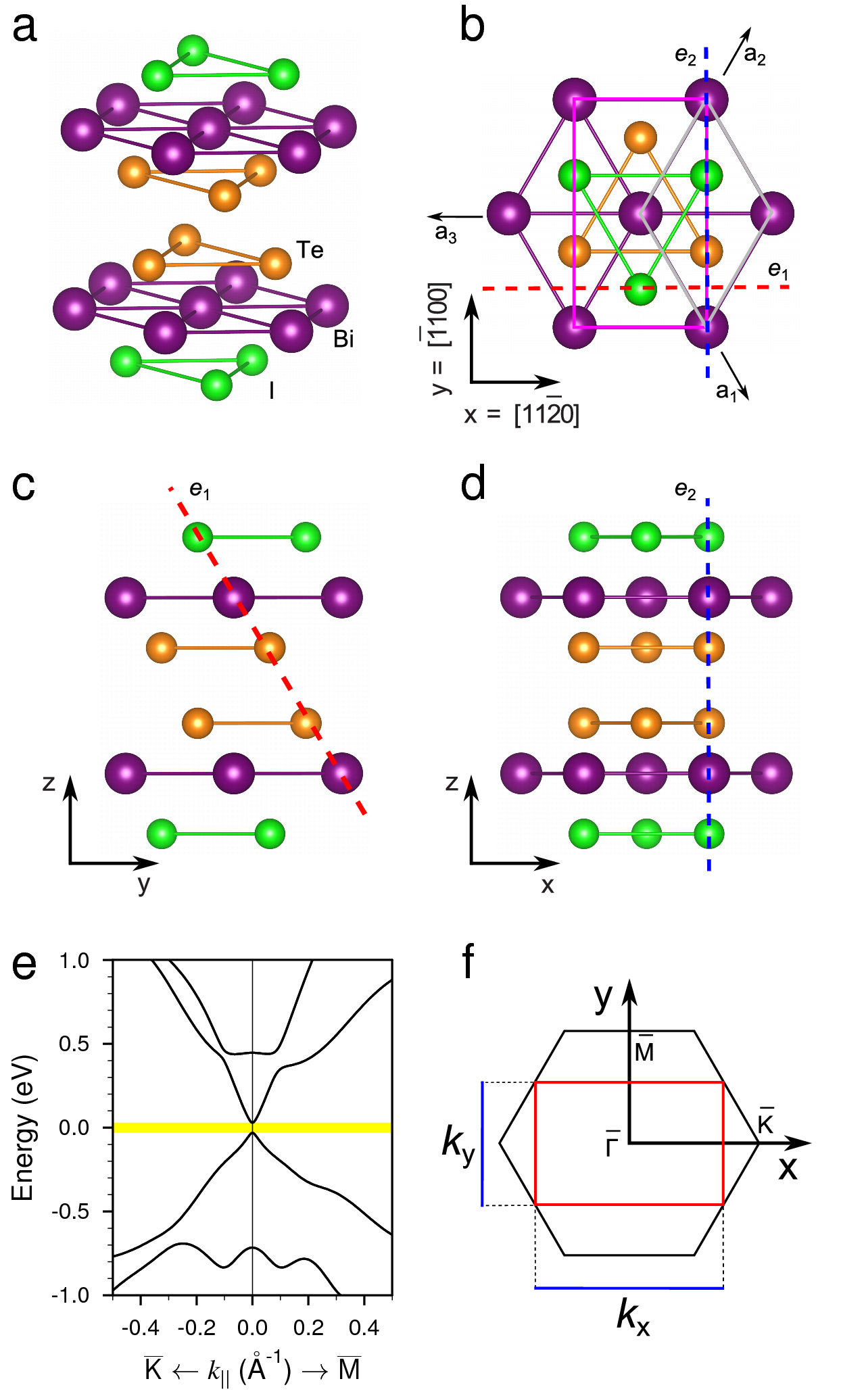
First we studied the energies of edges with different geometry to find out the most stable edge for the Bi2Te2I2-SL nanoribbon. We have considered stoichiometric mutually perpendicular cleavage planes and , see Fig 1(b–d). The plane is parallel to the () axis and crosses (0001) () plane at an angle of 56.96∘. The plane is parallel to the () axis and passes perpendicular to the (0001) plane. As expected from the effective continuous model,Linder the decay depth of the topological edge states in 2D TI should be much larger than that for the Dirac surface states in 3D TI. Consequently, to avoid the finite size effect, the nanoribbon width should be chosen as large as possible. We have constructed nanoribbons bounded by the two parallel and cleavage planes of the width of 150 Å. We found that the edge is by 170 meV/Å2 more favorable than the one. The stability of the edge looks reasonable, because the preferred cleavage plane is the one, which minimizes the number of broken bonds. The square of the plane is about 1.5 times smaller than that of the plane, while the number of broken bonds at the plane is two times bigger as compared to (8 and 4, respectively), and thus the density of the broken bonds (per unit square) is smaller for the edge. Note that the stoichiometric cleavage plane, similar to was found to be stable for the Bi2Te(Se)3 single quintuple layer (QL).Virk
Next, we examine the electronic structure of the ribbons with the and edges. Fig. 1(e) shows the spectrum of the Bi2Te2I2 film of single SL thickness calculated along high-symmetry directions of the hexagonal Brillouin zone [Fig. 1(f)]. As was demonstrated in Ref. Nechaev, this film has an inverted gap of 60 meV at the Fermi level, and in this gap (yellow stripe) we expect to find one-dimensional topological spin-helical states localized at the edge of the nanoribbon. When the () edge is formed, the 2D BZ of the Bi2Te2I2-SL is projected onto 1D BZ along the () direction [Fig. 1(f)].
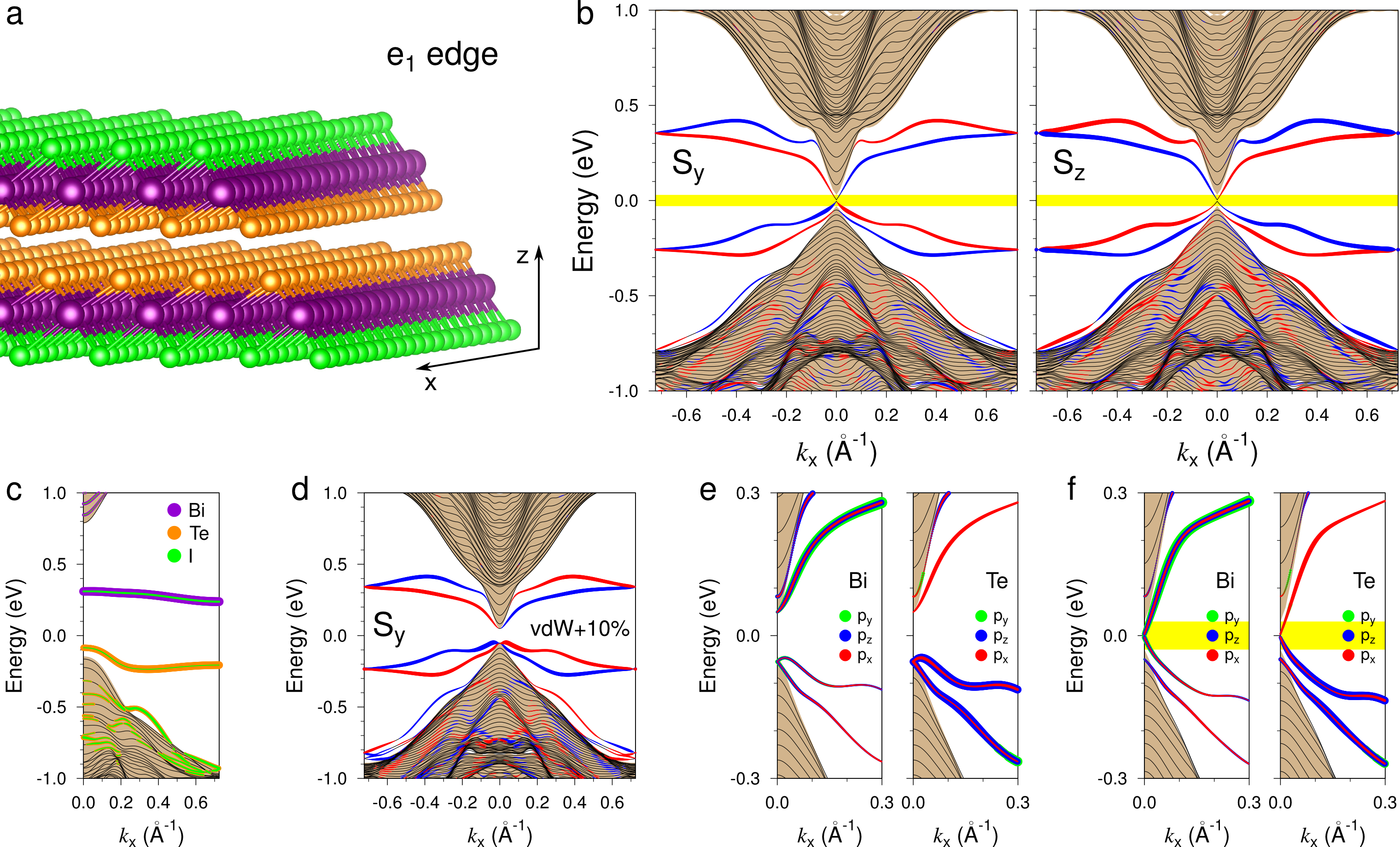
The calculated electronic structure of the ribbon (Fig. 2(a)) is shown in Fig. 2(b), where left and right panels demonstrate the same electronic spectrum but different projections of the spin expectation value for the localized states, and , which are orthogonal to the wave vector ( component of the spin is zero). They are calculated as a sum over atomic contributions from five near-edge atomic layers. As can be seen in Fig. 2(b), the spectrum has a gap at the Dirac point (of few meV) as the result of hybridization between edge states localized at the opposite edges of the ribbon despite we have chosen quite wide ribbon. Another observation is that beside the Dirac state the band structures also show the presence of a number of spin-polarized resonant states mainly in the valence band region as well as two trivial Rashba-split dangling bond states in the gap region far from the point. These states are originated from the broken bonds at the edge. With switched off spin-orbit coupling (SOC) these dangling bond states appear as two almost dispersionless bands [Fig. 2(c)]. The occupied and unoccupied bands have an only small iodine contribution and the former band is mainly contributed by Te orbitals, while the latter is primarily formed by the Bi orbitals. Both bands have character over 1D BZ that reflects the fact the dangling bonds are oriented perpendicular to the cleavage plane.
As was shown in Ref. Nechaev, , the vdW interaction between TLs that form the Bi2Te2I2-SL is crucial to realize QSHI phase. The gap in the SL spectrum closes at increasing the vdW spacing by 5% and further increase in the vdW spacing reopens trivial gap. At 10% expansion, the spectrum has the trivial gap of the width comparable to that in the equilibrium band-inverted SL.Nechaev Constructing the nanoribbon with the vdW spacing expanded by 10%, we found merely two dangling bond states acquired the Rashba splitting (Fig. 2(d), spin component is only shown). At large (0.3 Å-1) despite the spin splitting both bands keep their character, whereas at small [Fig. 2(e)] the orbital character is changed due to emergence of orbitals and the appearance of Bi states in the occupied band along with Te states in the unoccupied band. Comparing the orbital character of the Rashba-split dangling bond states near the point at the edge in trivial (vdW-expanded) SL with that in the QSHI [Fig. 2(f)], one can conclude that the emergent Dirac states have the atom-type contributions and the orbital compositions similar to that of trivial states, with which the Dirac states hybridize strongly.
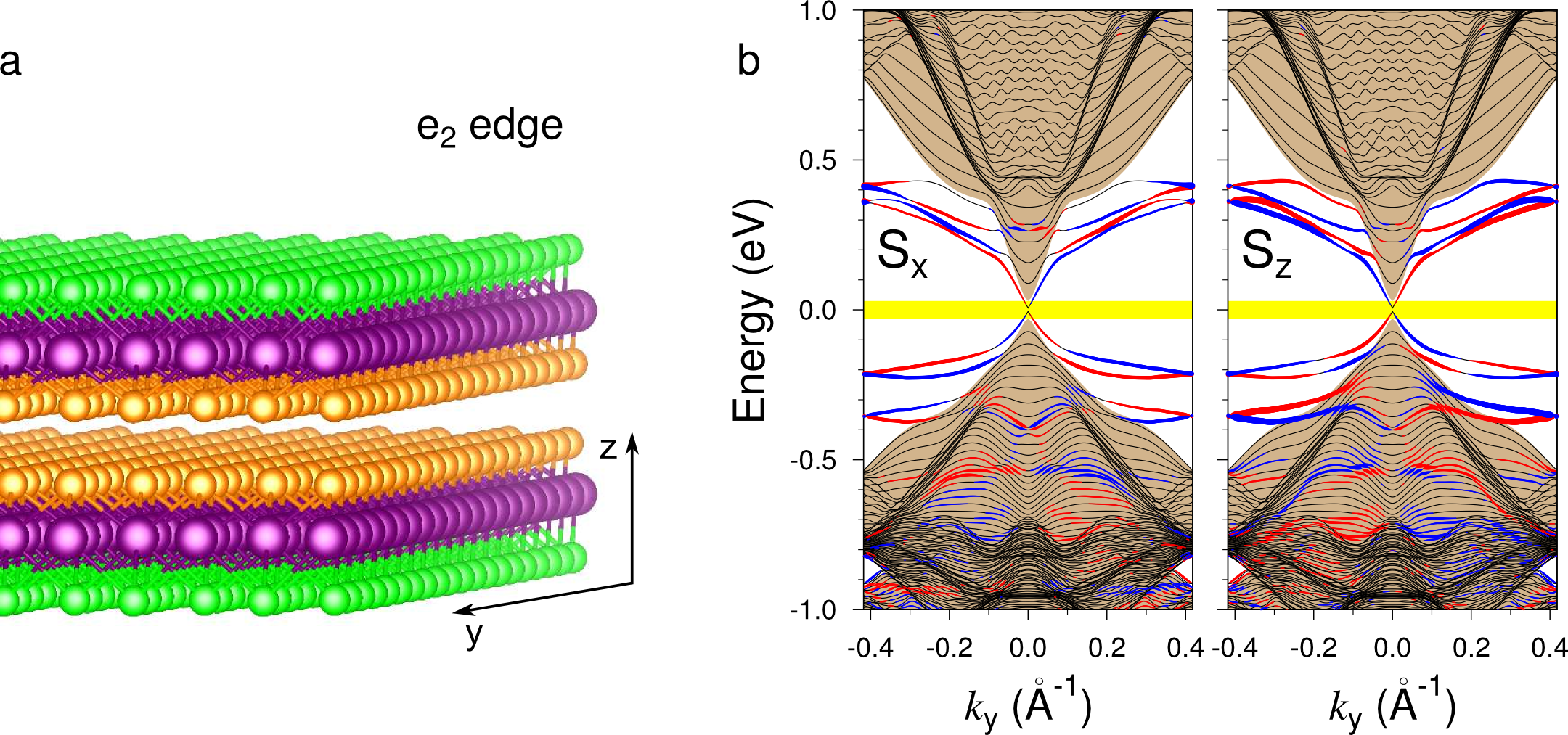
In the ribbon with the less stable edge [Fig. 3(a)], the spectrum and different spin projections, and ( is zero in this case) of which are presented in Fig. 3(b), additional expected trivial Rashba-split dangling bond states are emerged in the projected gap. The number of such bands is two times larger as compared to the spectrum of the edge owing to the fact that twice as many bonds break at the formation of this edge. However, as in the nanoribbon with edge, the dangling bond states lie far from the gap region (yellow stripe) where topological Dirac state resides.
III.2 Bi2Te2I2-SL 2D TI on BiTeI band insulator substrate
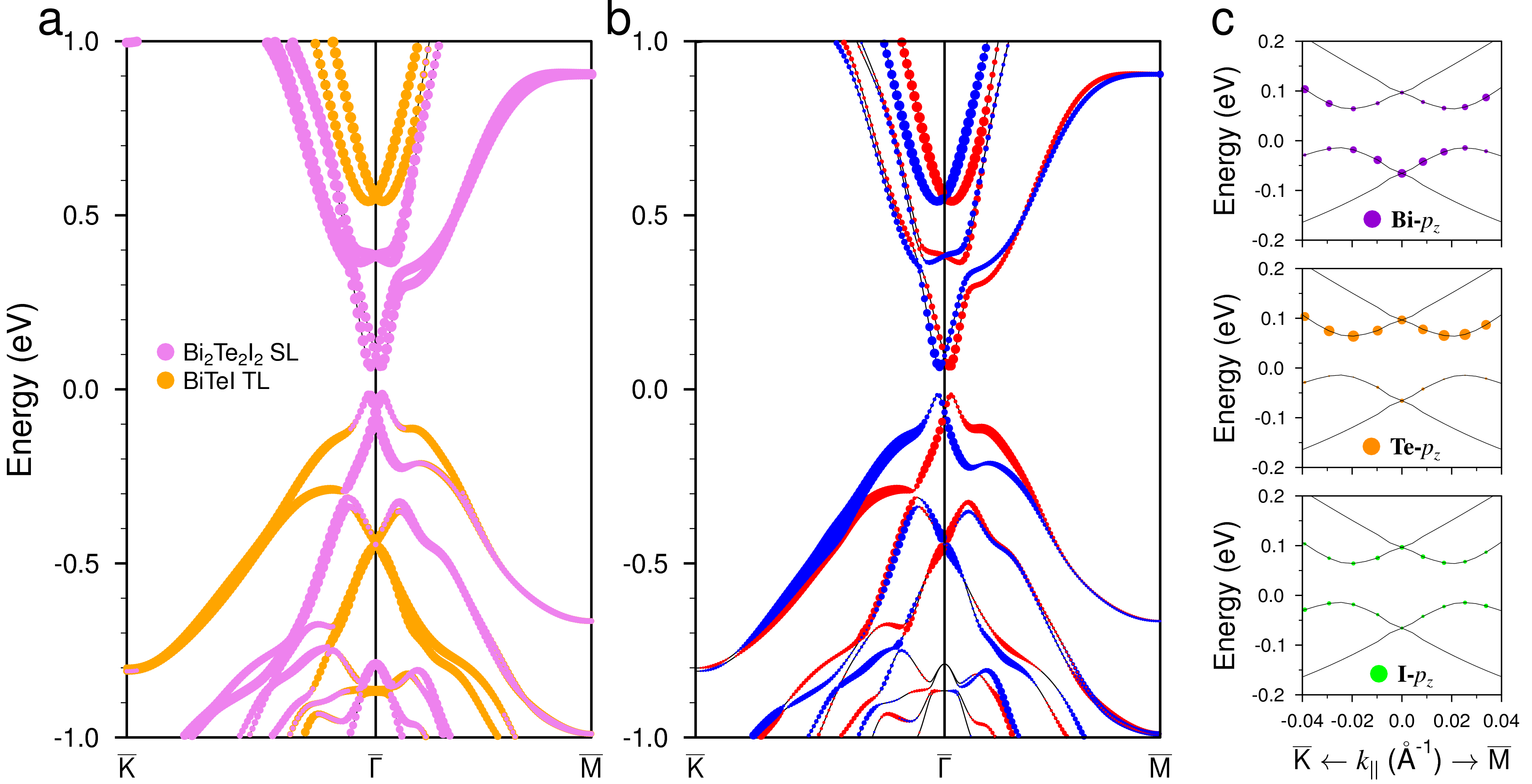
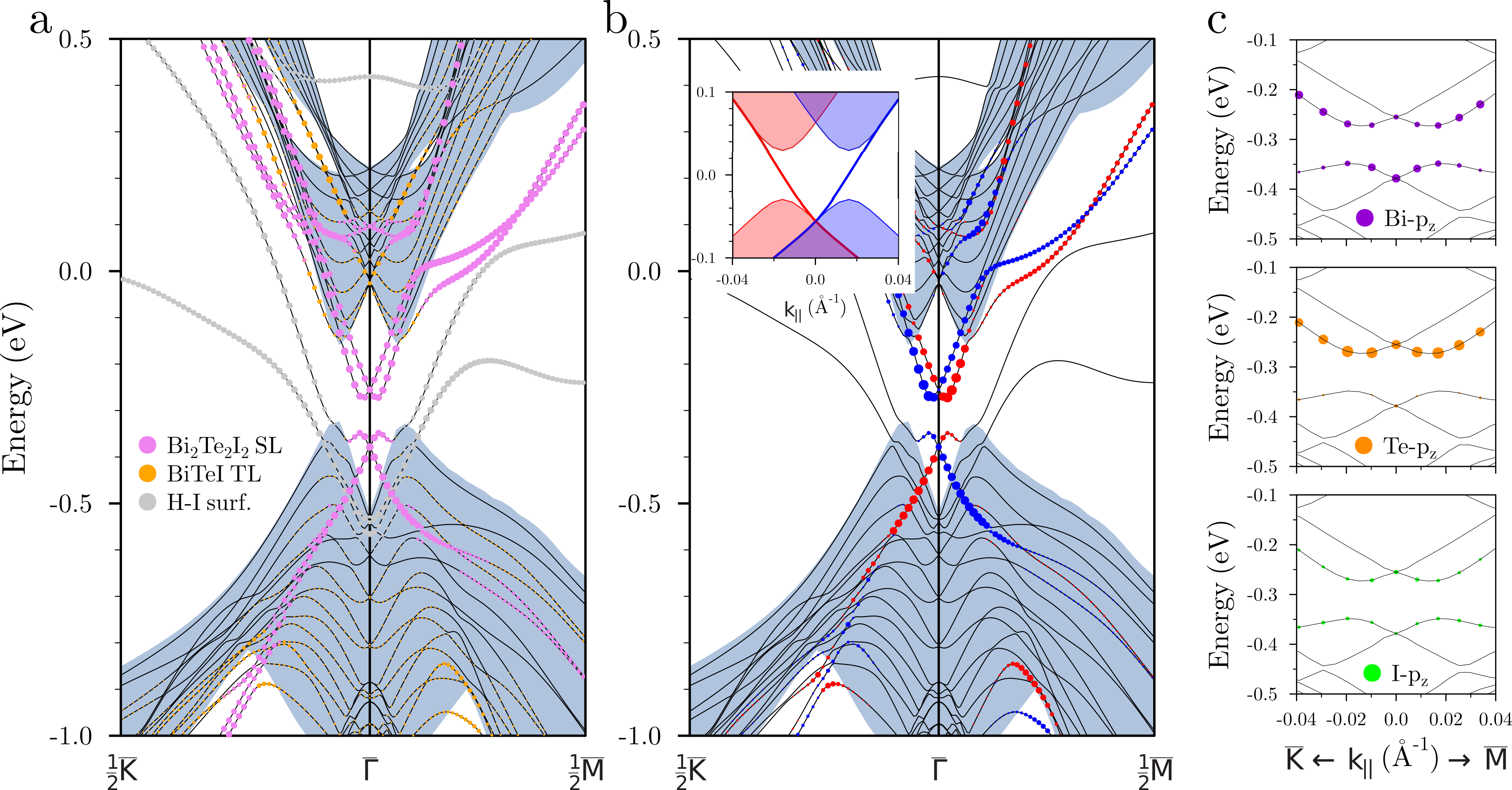
As we pointed above, one of the main challenge for 2D TIs is appropriate substrate, and the advantage of Bi2Te2I2 is that it has a natural substrate – BiTeI band insulator, which guarantees the absence of both the lattice mismatch and the interface charge transfer effects. Since the charge transfer is mostly a local effect, we consider first the structure composed of Bi2Te2I2-SL and a single BiTeI TL as [I-Bi-Te–Te-Bi-I]SL-[Te-Bi-I]TL. The calculated band spectrum of this structure is shown in Fig. 4. As can be seen in Fig. 4(a), the states forming a gap in this system belong to the Bi2Te2I2-SL, while the states localized in the BiTeI-TL lie far from the gap edges, especially in the unoccupied part of the spectrum. Since the [I-Bi-Te–Te-Bi-I]SL-[Te-Bi-I]TL system lacks the inversion symmetry, the states possess the Rashba spin-splitting (Fig. 4(b)). The splitting is almost isotropic with respect to , and splitting parameters are =0.026(0.020) Å-1 and =0.048(0.029) eV for valence (conduction) band. Beside the gap in Bi2Te2I2 states acquires the Rashba splitting, its width becomes larger. In the free-standing inversion symmetric Bi2Te2I2 the gap is of 60 meV (Fig. 1(e)), and in [I-Bi-Te–Te-Bi-I]SL-[Te-Bi-I]TL the absolute gap equals 78 meV (the -gap is ++). However, despite the Rashba splitting the gap-edge states remain inverted, as in the inversion symmetric Bi2Te2I2.Nechaev In the vicinity of , the Bi -orbitals mainly localized in the valence band, while Te orbitals dominate in the lowest conduction band (Fig. 4(c)). The calculation of for [I-Bi-Te–Te-Bi-I]SL-[Te-Bi-I]TL structure resulted in non-trivial topological invariant.
Next we increased the number of TLs in the slab so that the BiTeI part of the structure was sufficient to reproduce the BiTeI bulk. As in earlier works Eremeev_PRL2012 ; Landolt_PRL2012 ; Eremeev_JETPLett2012 we used BiTeI slab of 8 TLs thickness with the back, iodine-terminated, surface passivated by hydrogen. As can be seen in Fig. 5(a,b), in Bi2Te2I2-SL@BiTeI heterostructure the Bi2Te2I2 states lie within the BiTeI bulk gap. The gap in Bi2Te2I2 states =74 meV is almost the same as in case of single TL BiTeI substrate but spin-splitting parameters became slightly smaller: =0.018(0.014) Å-1 and =0.030(0.018) eV for valence (conduction) band. Such small alterations in the Bi2Te2I2 spectrum in the vicinity of do not affect the gap inversion as can be seen in Fig. 5(c). As before, the gap edges are mainly formed by orbitals of Bi (VB) and Te (CB) atoms.
Thus, 2D TI Bi2Te2I2 survives on BiTeI substrate. This is due to the fact that Bi2Te2I2 and BiTeI are actually the same materials, which differ in TLs staking order only. It guarantees the absence of the interface potential because the interface [I-Bi-Te–Te-Bi-I]SL-[Te-Bi-I]-[Te-Bi-I]-… can be regarded as the structure [I-Bi-Te]-[Te-Bi-I]-[Te-Bi-I]-[Te-Bi-I]-…, i.e., as the BiTeI surface, where uppermost TL has inverted atomic layer sequence. The splitting in the spin subbands in the 2D TI Bi2Te2I2 spectrum on the BiTeI substrate will result in the opposite -shifting of the corresponding spin branches of the Dirac state in the 1D spectrum as schematically shown in the inset in Fig. 5(b). Wherein, the Dirac point that is in the middle of the gap in the case of free-standing SL might be shifted downward to the region of the two-dimensional states.
III.3 Search for 2D and 3D topological phases in Bi2Te2Br2 and Bi2Te2Cl2
Finally, we consider 2D and 3D centrosymmetric phases constructed from TLs of the related band insulators BiTeBr and BiTeCl. Despite the bulk stacking faults, which is a key element for centrosymmetric BiTe pases, are missing in BiTeBr and BiTeCl obtained by the Bridgeman method as follows from the experimentFiedler_PRB2015 demonstrating the absence of the mixed-terminated surfaces in these materials, however, one can assume that centrosymmetric films of BiTeBr and BiTeCl can, in principle, be epitaxially grown.
Calculating the total energies of free-standing SLs of Bi2Te2Br2 and Bi2Te2Cl2 we found that they have lower (by 98 and 91 meV, respectively) energies than BiTeBr and BiTeCl films of double TL thickness have. However, the bulk phases composed of Bi2Te2Br2 and Bi2Te2Cl2 SLs are less favorable as compared to corresponding BiTeBr and BiTeCl non-centrosymmetric bulk crystals. The energy losing for Bi2Te2Br2 with respect to BiTeBr is 20.75 meV per BiTeI fu and it is 26.35 meV/fu for Bi2Te2Cl2 system in comparison with BiTeCl.
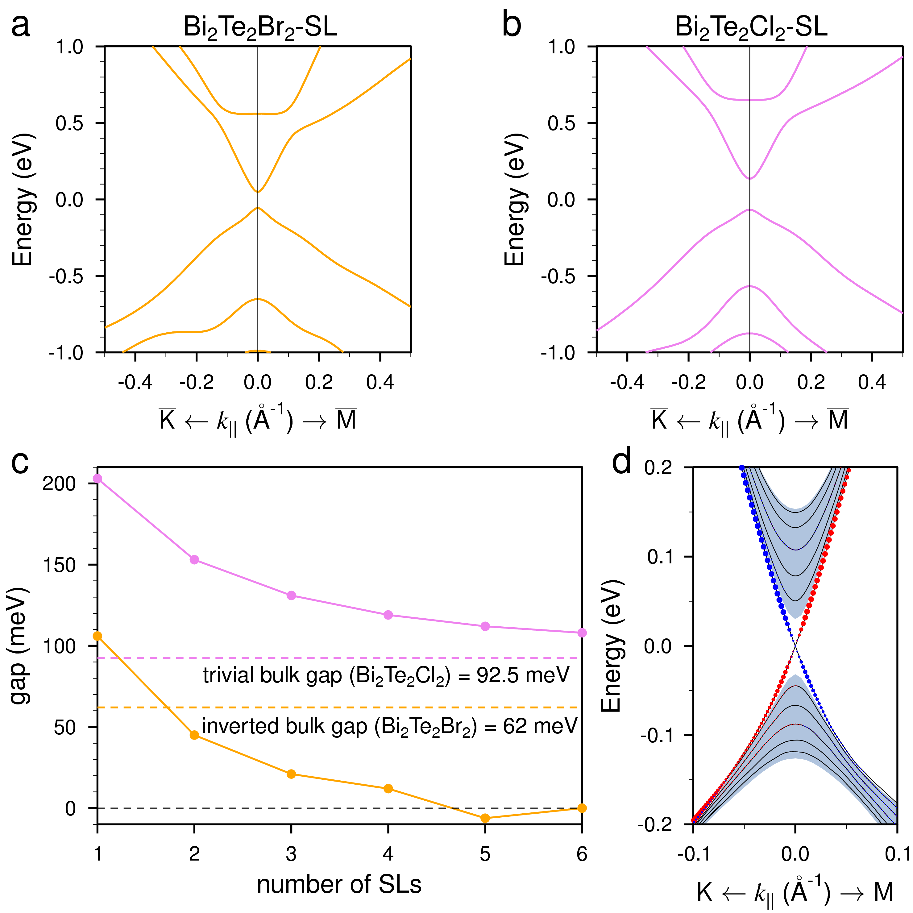
The band spectra of Bi2Te2Br2 and Bi2Te2Cl2 single, free-standing SLs [Fig. 6(a,b)], in general, are similar to that of Bi2Te2I2, however, they have larger band gaps, 106 and 203 meV, respectively, and, according to calculations, these centrosymmetric Bi2Te2Br2 and Bi2Te2Cl2 SLs are topologically trivial.
Next, like the case of Bi2Te2I2, we addressed the electronic structure of the Bi2Te2Br2 and Bi2Te2Cl2 bulk. We revealed that Bi2Te2Br2 has an inverted band gap of 62 meV while Bi2Te2Cl2 bulk is a trivial band insulator with the gap of 92.5 meV and thus it is trivial in both 2D and 3D phases.
Considering the dependence of the -gap and the topological invariant on the film thickness for Bi2Te2Br2 and Bi2Te2Cl2 [Fig. 6(c)], we found that in contrast to Bi2Te2I2 where along with a sharp decrease in the value of the gap, the oscillating behavior of with the number of SLs was obtained, Nechaev the Bi2Te2Cl2 demonstrates a smooth decrease in the gap to its bulk value, remaining at any film thickness the trivial insulator, while Bi2Te2Br2 at the five-SL thickness becomes a 2D TI with the small inverted gap of 6 meV. For thicker films, the gap is zero that indicates on the converged Dirac cone of the 3D TI phase. The surface spectrum of latter is shown in Fig. 6 (d).
IV Conclusions
In summary, by using first-principles calculations we have examined the topologically protected edge states and topologically trivial Rashba-split spin-polarized dangling bond states emerged at the different edges of the 2D topological insulator Bi2Te2I2 of one-sextuple-layer thickness. We have revealed that irrespective of the edge plane the dangling bond states lie rather far from the 2D band projected gap energy region, where the Dirac state resides. We also suggested the appropriate substrate for 2D Bi2Te2I2 QSHI, which is parental non-centrosymmetric BiTeI compound. This substrate guarantees the absence of both lattice mismatch and interface charge transfer effects. Since BiTeI is the material with the giant Rashba-type spin splitting, it produces a sizable spin splitting in 2D band structure of QSHI film. However, despite the Rashba splitting in the states forming the gap the latter remains inverted, and the 2D topological phase survives in Bi2Te2I2/BiTeI heterostructure as confirmed from the index calculation. We also systematically examined the possibility of realizing nontrivial 2D and 3D topological phases in thin films and bulk crystals of related hypothetical compounds composed of centrosymmetric sextuple layers of BiTeBr and BiTeCl. We have revealed that ultra thin centrosymmetric films of Bi2Te2Br2 are trivial band insulators up to five-SL thickness, and in the 3D limit Bi2Te2Br2 is a strong TI, while both 2D and 3D phases of Bi2Te2Cl2 are topologically trivial. We hope that our study will motivate further experimental works on topologically non-trivial centrosymmetric BiTe systems.
This work was supported by the Spanish Ministry of Economy and Competitiveness MINECO (Project No. FIS2016-76617-P) and Saint Petersburg State University (Grant No. 15.61.202.2015).
References
- (1) C.L. Kane, and E.J. Mele, topological order and the quantum spin Hall effect Phys. Rev. Lett. 95, 146802 (2005).
- (2) B.A. Bernevig, and S.-C. Zhang, Quantum spin Hall effect Phys. Rev. Lett. 96, 106802 (2006).
- (3) B.A. Bernevig, T.L. Hughes, and S.-C. Zhang, Quantum spin Hall effect and topological phase transition in HgTe quantum wells Science 314, 1757 (2006).
- (4) M. König, S. Wiedmann, C. Brüne, A. Roth, H. Buhmann, L.W. Molenkamp, X.L. Qi, and S.-C. Zhang, Quantum spin Hall insulator state in HgTe quantum wells Science 318, 766 (2007).
- (5) I. Knez, R.-R. Du, and G. Sullivan, Evidence for Helical Edge Modes in Inverted InAs/GaSb Quantum Wells, Phys. Rev. Lett. 107, 136603 (2011).
- (6) Y. Ren, Z. Qiao, and Q. Niu, Topological phases in two-dimensional materials: a review Rep. Prog. Phys. 79, 066501 (2016).
- (7) I.K. Drozdov, A. Alexandradinata, S. Jeon, S. Nadj-Perge, H. Ji, R.J. Cava, B. Bernevig, and Ali Yazdani, One-dimensional topological edge states of bismuth bilayers Nature Physics 10, 664 (2014).
- (8) Y. Lu, W. Xu, M. Zeng, G. Yao, L. Shen, M. Yang, Z. Luo, F. Pan, K. Wu, T. Das, P. He, J. Jiang, J. Martin, Y.P. Feng, H. Lin, and X.-s. Wang, Topological Properties Determined by Atomic Buckling in Self- Assembled Ultrathin Bi(110) Nano Lett. 15, 80 (2015).
- (9) Sung Hwan Kim, Kyung-Hwan Jin, Joonbum Park, Jun Sung Kim, Seung-Hoon Jhi, and Han Woong Yeom, Topological phase transition and quantum spin Hall edge states of antimony few layers, Sci. Rep. 6, 33193 (2016).
- (10) Xiang-Bing Li, Wen-Kai Huang, Yang-Yang Lv, Kai-Wen Zhang, Chao-Long Yang, Bin-Bin Zhang, Y. B. Chen, Shu-Hua Yao, Jian Zhou, Ming-Hui Lu, Li Sheng, Shao-Chun Li, Jin-Feng Jia, Qi-Kun Xue, Yan-Feng Chen, and Ding-Yu Xing, Experimental Observation of Topological Edge States at the Surface Step Edge of the Topological Insulator ZrTe5, Phys. Rev. Lett. 116, 176803 (2016).
- (11) R. Wu, J.-Z. Ma, S.-M. Nie, L.-X. Zhao, X. Huang, J.-X. Yin, B.-B. Fu, P. Richard, G.-F. Chen, Z. Fang, X. Dai, H.-M. Weng, T. Qian, H. Ding, and S. H. Pan, Evidence for Topological Edge States in a Large Energy Gap near the Step Edges on the Surface of ZrTe5, Phys. Rev. X 6, 021017 (2016).
- (12) I.A. Nechaev, S.V. Eremeev, E.E. Krasovskii, P.M. Echenique, and E.V. Chulkov, Quantum spin Hall insulators in centrosymmetric thin films composed from topologically trivial BiTeI trilayers Sci. Rep. 7, 43666 (2017).
- (13) K. Ishizaka, M. S. Bahramy, H. Murakawa, M. Sakano, T. Shimojima, T. Sonobe, K. Koizumi, S. Shin, H. Miyahara, A. Kimura, K. Miyamoto, T. Okuda, H. Namatame, M. Taniguchi, R. Arita, N. Nagaosa, K. Kobayashi, Y. Murakami, R. Kumai, Y. Kaneko, Y. Onose and Y. Tokura, Giant Rashba-type spin splitting in bulk BiTeI, Nature Mater. 10, 521 (2011).
- (14) S. V. Eremeev, I. A. Nechaev, Yu. M. Koroteev, P. M. Echenique, and E. V. Chulkov, Ideal two-Dimensional electron systems with a giant Rashba-type spin splitting in real materials: surfaces of bismuth tellurohalides, Phys. Rev. Lett. 108, 246802 (2012).
- (15) A. Crepaldi, L. Moreschini, G. Autès, C. Tournier-Colletta, S. Moser, N. Virk, H. Berger, Ph. Bugnon, Y. J. Chang, K. Kern, A. Bostwick, E. Rotenberg, O. V. Yazyev, and M. Grioni, Giant Ambipolar Rashba Effect in the Semiconductor BiTeI, Phys. Rev. Lett. 109, 096803 (2012).
- (16) G. Landolt, S.V. Eremeev, Yu.M. Koroteev, B. Slomski, S. Muff, T. Neupert, M. Kobayashi, V.N. Strocov, T. Schmitt, Z.S. Aliev, M.B. Babanly, I.R. Amiraslanov, E.V. Chulkov, J. Osterwalder, and J.H. Dil, Disentanglement of Surface and Bulk Rashba Spin Splittings in Noncentrosymmetric BiTeI Phys. Rev. Lett. 109, 116403 (2012).
- (17) S.V. Eremeev, I.A. Nechaev, and E.V. Chulkov, Giant Rashba-type spin splitting at polar surfaces of BiTeI JETP Lett. 96, 437 (2012).
- (18) S.V. Eremeev, I.P. Rusinov, I.A. Nechaev, and E.V. Chulkov, Rashba split surface states in BiTeBr New J. Phys. 15, 075015 (2013).
- (19) G. Landolt, S.V. Eremeev, O.E. Tereshchenko, S. Muff, B. Slomski, K.A. Kokh, M. Kobayashi, T. Schmitt, V.N. Strocov, J. Osterwalder, E.V. Chulkov, and J.H. Dil, Bulk and surface Rashba splitting in single termination BiTeCl New J. Phys. 15, 085022 (2013).
- (20) M. Sakano, M. S. Bahramy, A. Katayama, T. Shimojima, H. Murakawa, Y. Kaneko, W. Malaeb, S. Shin, K. Ono, H. Kumigashira, R. Arita, N. Nagaosa, H. Y. Hwang, Y. Tokura, and K. Ishizaka, Strongly Spin-Orbit Coupled Two-Dimensional Electron Gas Emerging near the Surface of Polar Semiconductors Phys. Rev. Lett. 110, 107204 (2013).
- (21) I.P. Rusinov, I.A. Nechaev, S.V. Eremeev, C. Friedrich, S. Blügel, and E. V. Chulkov, Many-body effects on the Rashba-type spin splitting in bulk bismuth tellurohalides Phys. Rev. B 87, 205103 (2013).
- (22) J. Mauchain, Y. Ohtsubo, M. Hajlaoui, E. Papalazarou, M. Marsi, A. Taleb-Ibrahimi, J. Faure, K. A. Kokh, O. E. Tereshchenko, S.V. Eremeev, E.V. Chulkov, and L. Perfetti, Circular Dichroism and Superdiffusive Transport at the Surface of BiTeI, Phys. Rev. Lett. 111, 126603 (2013).
- (23) C.J. Butler, H.-H. Yang, J.-Y. Hong, S.-H. Hsu, R. Sankar, C.-I. Lu, H.-Y. Lu, K.-H. O. Yang, H.-W. Shiu, C.-H. Chen, C.-C. Kaun, G.-J. Shu, F.-C. Chou, and M.-T. Lin, Mapping polarization induced surface band bending on the Rashba semiconductor BiTeI Nature Commun. 5, 4066 (2014).
- (24) C. Tournier-Colletta, G. Autès, B. Kierren, Ph. Bugnon, H. Berger, Y. Fagot-Revurat, O.V. Yazyev, M. Grioni, and D. Malterre, Atomic and electronic structure of a Rashba junction at the BiTeI surface Phys. Rev. B 89, 085402 (2014).
- (25) M. K. Tran, J. Levallois, P. Lerch, J. Teyssier, A. B. Kuzmenko, G. Autès, O. V. Yazyev, A. Ubaldini, E. Giannini, D. van der Marel, and A. Akrap, Infrared- and Raman-Spectroscopy Measurements of a Transition in the Crystal Structure and a Closing of the Energy Gap of BiTeI under Pressure, Phys. Rev. Lett. 112, 047402 (2014).
- (26) Sebastian Fiedler, Lydia El-Kareh, Sergey V. Eremeev, Oleg E. Tereshchenko, Christoph Seibel, Peter Lutz, Konstantin A. Kokh, Evgueni V. Chulkov, Tatyana V. Kuznetsova, Vladimir I. Grebennikov, Hendrik Bentmann, Matthias Bode and Friedrich Reinert, Defect and structural imperfection effects on the electronic properties of BiTeI surfaces, New J. Phys. 16, 075013 (2014).
- (27) S. Fiedler, T. Bathon, S.V. Eremeev, O.E. Tereshchenko, K.A. Kokh, E.V. Chulkov, P. Sessi, H. Bentmann, M. Bode, and F. Reinert, Termination-dependent surface properties in the giant-Rashba semiconductors BiTe ( = Cl , Br, I) Phys. Rev. B 92, 235430 (2015).
- (28) I. P. Rusinov, T. V. Menshchikova, I. Yu. Sklyadneva, R. Heid, K.-P. Bohnen and E. V. Chulkov, Pressure effects on crystal and electronic structure of bismuth tellurohalides, New J. Phys. 18, 113003 (2016).
- (29) H. Maaß, H. Bentmann, C. Seibel, C. Tusche, S. V. Eremeev, T. R. F. Peixoto, O. E. Tereshchenko, K. A. Kokh, E. V. Chulkov, J. Kirschner, and F. Reinert, Spin-texture inversion in the giant Rashba semiconductor BiTeI Nature Commun. 7, 11621 (2016).
- (30) S.V. Eremeev, S.S. Tsirkin, I.A. Nechaev, P.M. Echenique, and E.V. Chulkov, New generation of two-dimensional spintronic systems realized by coupling of Rashba and Dirac fermions, Sci. Rep. 5, 12819 (2015).
- (31) G. Bihlmayer, Yu. M. Koroteev, T. V.Menshchikova, E. V. Chulkov, and Stefan Blügel, Ab Initio Calculations of Two-Dimensional Topological Insulators in Topological Insulators, Fundamentals and Perspectives (Wiley-VCH Verlag GmbH & Co. KGaA, Weinheim, 2015).
- (32) T. Förster, P. Krüger, and M. Rohlfing, Two-dimensional topological phases and electronic spectrum of Bi2Se3 thin films from calculations, Phys. Rev. B 92, 201404(R) (2015).
- (33) T. Förster, P. Krüger, and M. Rohlfing, calculations for and thin films: Electronic and topological properties, Phys. Rev. B 93, 205442 (2016).
- (34) I. A. Nechaev and E. E. Krasovskii, Relativistic Hamiltonians for centrosymmetric topological insulators from ab initio wave functions, Phys. Rev. B 94, 201410 (2016).
- (35) V. N. Men shov, V. V. Tugushev, and E. V. Chulkov, Spin Hall Conductivity in Three-Dimensional Topological Insulator/Normal Insulator Heterostructures, JETP Letters 102, 754 (2015).
- (36) A. Takayama, T. Sato, S. Souma, T. Oguchi, and T. Takahashi, One-Dimensional Edge States with Giant Spin Splitting in a Bismuth Thin Film Phys. Rev. Lett. 114, 066402 (2015).
- (37) T. Hirahara, G. Bihlmayer, Y. Sakamoto, M. Yamada, H. Miyazaki, S.-i. Kimura, S. Blügel, and S. Hasegawa, Interfacing 2D and 3D Topological Insulators: Bi(111) Bilayer on Bi2Te3 Phys. Rev. Lett. 107, 166801 (2011).
- (38) F.-C. Chuang, L.-Z. Yao, Z.-Q. Huang, Y.-T. Liu, C.-H. Hsu, T. Das, H. Lin, and A. Bansil, Prediction of Large-Gap Two-Dimensional Topological Insulators Consisting of Bilayers of Group III Elements with Bi Nano Lett. 14, 2505 (2014).
- (39) M. Zhou, W. Ming, Z. Liu, Z. Wang, P. Li, and F. Liu, Epitaxial growth of large-gap quantum spin Hall insulator on semiconductor surface Proc. Natl Acad. Sci. 111, 14378 (2014).
- (40) M. Zhou, W. Ming, Z. Liu, Z. Wang, Y. Yao and F. Liu, Formation of quantum spin Hall state on Si surface and energy gap scaling with strength of spin orbit coupling Sci. Rep. 4, 7102 (2014).
- (41) C.-H. Hsu, Z.-Q. Huang, F.-C. Chuang, C.-C. Kuo, Y.-T. Liu, H. Lin, and A. Bansil, The nontrivial electronic structure of Bi/Sb honeycombs on SiC(0001) New J. Phys. 17, 025005 (2015).
- (42) Z.-Q. Huang, B.-H. Chou, C.-H. Hsu, F.-C. Chuang, H. Lin, and A. Bansil, Tunable topological electronic structure of silicene on a semiconducting Bi/Si(111)- substrate Phys. Rev. B 90, 245433 (2014).
- (43) Z.-Q. Huang, F.-C. Chuang, C.-H. Hsu, Y.-T. Liu, H.-R. Chang, H. Lin, and A. Bansil, Nontrivial topological electronic structures in a single Bi(111) bilayer on different substrates: a first-principles study Phys. Rev. B 88, 165301 (2013).
- (44) Z. Song, C.-C. Liu, J. Yang, J. Han, M. Ye, B. Fu, Y. Yang, Q. Niu, J. Lu, and Y. Yao, Quantum spin Hall insulators and quantum valley Hall insulators of BiX/SbX (X=H, F, Cl and Br) monolayers with a record bulk band gap NPG Asia Materials 6, e147 (2014).
- (45) F.-C. Chuang, C.-H. Hsu, H.-L. Chou, C.P. Crisostomo, Z.-Q. Huang, S.-Y. Wu, C.-C. Kuo, W.-C. V. Yeh, H. Lin, and A. Bansil, Prediction of two-dimensional topological insulator by forming a surface alloy on Au/Si(111) substrate Phys. Rev. B 93, 035429 (2016).
- (46) P.E. Blöchl, Projector augmented-wave method, Phys. Rev. B 50, 17953 (1994).
- (47) G. Kresse, D. Joubert, From ultrasoft pseudopotentials to the projector augmented-wave method, Phys. Rev. B 59, 1758 (1999).
- (48) G. Kresse, J. Hafner, Ab initio molecular dynamics for open-shell transition metals, Phys. Rev. B 48, 13115 (1993).
- (49) G. Kresse, J. Furthmüller, Efficient iterative schemes for ab initio total-energy calculations using a plane-wave basis set, Phys. Rev. B 54, 11169 (1996).
- (50) S. Grimme, J. Antony, S. Ehrlich, and H. Krieg, A consistent and accurate ab initio parametrization of density functional dispersion correction (DFT-D) for the 94 elements H-Pu, J. Chem. Phys. 132, 154104 (2010).
- (51) A.A. Soluyanov, and D. Vanderbilt, Computing topological invariants without inversion symmetry Phys. Rev. B 83, 235401 (2011).
- (52) Jacob Linder, Takehito Yokoyama, and Asle Sudbø, Anomalous finite size effects on surface states in the topological insulator Bi2Se3, Phys. Rev. B 80, 205401 (2009).
- (53) N. Virk, and O.V. Yazyev, Dirac fermions at highindex surfaces of bismuth chalcogenide topological insulator nanostructures Sci. Rep. 6, 20220 (2016).