Near-unity collection efficiency from quantum emitters in bulk diamond using chirped circular dielectric gratings
Abstract
Efficient collection of fluorescence from nitrogen vacancy (NV) centers in diamond underlies the spin-dependent optical read-out that is necessary for quantum information processing and enhanced sensing applications. The optical collection efficiency from NVs within diamond substrates is limited primarily due to the high refractive index of diamond and the non-directional dipole emission. Here we introduce a light collection strategy based on chirped, circular dielectric gratings that can be fabricated on a bulk diamond substrate to redirect an emitter’s far-field radiation pattern. Using a genetic optimization algorithm, these grating designs achieve 98.9% collection efficiency for the NV zero-phonon emission line, collected from the back surface of the diamond with an objective of aperture 0.9. Across the broadband emission spectrum of the NV (600-800 nm), the chirped grating achieves 82.2% collection efficiency into a numerical aperture of 1.42, corresponding to an oil immersion objective again on the back side of the diamond. Our proposed bulk-dielectric grating structures are applicable to other optically active solid state quantum emitters in high index host materials.
Department of Electrical Engineering and Computer Science, Massachusetts Institute of Technology, Cambridge, Massachusetts 02139, USA. \abbreviationsIR,NMR,UV
Keywords: collection efficiency, grating, nitrogen vacancy center, quantum enhanced metrology
Introduction
The negatively charged nitrogen vacancy (NV) center in diamond has emerged as a leading semiconductor quantum system with well-controlled electronic orbitals and spin states. A number of applications are being developed, including quantum computation 1, 2, quantum networking 3, quantum simulation4, quantum error correction 5 and precision sensing6, 7, 8. There has also been considerable progress in developing other atom-like quantum emitters in solids with unique features.9, 10, 11, 12, 13, 14, 15, 16, 17
The efficient collection of fluorescence emitted by individual quantum emitters is of central importance in advancing these quantum technologies. For instance, the photon collection efficiency of the NV’s total emission (zero phonon line and phonon side-band) determines the minimum detectable magnetic field with a single NV as 18, 19, 20, assuming photon shot-noise limited detection. The total NV fluorescence collection efficiency is also essential for fast syndrome measurements in quantum error correction 5. In quantum networking, the rate at which two NV centers can be optically entangled depends on how efficiently two identical photons can be detected, so that the rate is proportional to . Higher collection efficiency is necessary to allow the entanglement generation rate to exceed the decoherence rate of the NV.
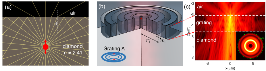
Efficient collection of NV fluorescence remains challenging and is hindered primarily by two factors: (1) The dipolar emission pattern of NV fluorescence21 is challenging to efficiently collect with a single port 22; (2) The large refractive index mismatch between diamond ( 2.41 at 637 nm) and air confines the emitted photons by total internal reflection (TIR), allowing only a small fraction of the emission to couple out. These two reasons set the collection efficiency of a point source (shown in Fig.1(a)) to a baseline value of , where 0.8 is the approximate averaged Fresnel transmission coefficient for diamond-air interface within the TIR window. (See Supporting Information section S2 for a rigorous calculation on the baseline values of collection efficiency for a dipole emitter). In addition, the NV photon generation rate is relatively low mainly because of its rather long excited state lifetime ( 13 ns) 23; (See Supporting Information section S1 for estimation of NV- intrinsic emission rate). This lifetime could be reduced using the Purcell effect. However, simply enhancing the NV emission rate via Purcell effect is likely to decrease the spin readout contrast, as recently discussed theoretically24 and experimentally 25.
To tackle those challenges, various optical structures have been investigated, including tapered fibers26, metallic mirrors placed in close proximity to NV 27, nanofabricated solid immersion lenses 28, 29, parabolic mirrors30, nanowire arrays 31, dielectric optical antennas32, hybrid waveguide structures 33, diamond-silver apertures34 and plasmonic gratings 35.
In this work, we consider bullseye gratings that consist of a series of concentric circular rings dry-etched into diamond with an NV in the center. Circularly symmetric structures are generally preferred because they eliminate the need for alignment to the dipole orientation of the emitter. Circular gratings have previously been considered for cavity-defect mode enhancement36, high-Q resonators 37, and emission out-coupling of quantum dots38, 39. Experiments with circular gratings on a diamond membrane have shown measured single NV photon count rates of 3 Mcps 40.
An important challenge in imposing a grating on a bulk dielectric surface relates to the pitch of the air slits. In a thin membrane supporting only the fundamental mode in the vertical direction, a constant-period pitch works well38, 40. For a bulk dielectric medium, however, the grating needs to accommodate a range of -values in the out-of-plane direction. In this case, a non-periodic, chirped grating provides better coupling into a target out-of-plane propagating mode. The chirped grating approach can also improve the coupling efficiency over a broad spectral range, whereas constant-period gratings are optimal for narrowband operation. Chirped optical structures have been developed for applications that require broad bandwidth and wide angular range operations, such as broadband mirrors for ultrafast lasers41, or ultra-thin photovoltaic devices with enhanced absorption42, 43. Additionally, implementing the chirped circular structure on a relatively thick diamond film ( 20 m) instead of on a single mode diamond membrane ( 200 nm) could further improve the collection efficiency by index guiding44. Finally, a mirror can be placed on the top side of the grating to reflect the upwards-propagating emission and help cover a complete range of -values.
The chirped circular grating structures introduced here enable near-unity collection efficiency into the detection apparatus for different numerical aperture (NA). These bulk-dielectric grating structures can be fabricated in bulk diamond and do not require diamond membranes, which are not commercially available and difficult to fabricate45, 46, 47. We numerically evaluate the performance of chirped circular gratings optimized for three specific detection schemes:
-
(a)
Collection of the NV’s zero-phonon line (ZPL) through an objective lens under cryogenic conditions, as required for photonic entanglement of remote NV centers;
-
(b)
Collection of the phonon side band (PSB) through an objective lens under cryogenic conditions, as required for quantum state estimation and quantum error correction;
-
(c)
Collection of the NV’s ZPL and PSB through an oil immersion objective lens at room temperature, as required for many quantum-enhanced sensing applications.
For detection scheme (a), the chirped bulk-dielectric grating achieves a near-unity collection efficiency of 98.9% into an NA of 0.9 air objective (Bullseye grating A), corresponding to a 275 fold improvement in collection efficiency compared to unpatterned diamond. For scheme (b), we predict a collection efficiency of 68.8% for the broad PSB emission with same Bullseye grating A . In scheme (c), a chirped circular grating optimized for broadband efficient collection (Bullseye grating B) yields an averaged collection efficiency of 82.2% into NA = 1.42 and averaged Purcell factor of 1.18. We also examine the sensitivities of the collection efficiency enhancements for NV displacement from the optimal position. For grating A, the enhancement stays within 15.9% of the maximum as long as the NV is within 20 nm from its ideal position. Our chirped circular grating promises high collection efficiency with moderate Purcell factors for emitters embedded in a high index host material. The chirped circular grating is flexible in design for different experimental conditions, has negligible photon loss compared to plasmonic gratings, is relatively robust to NV position errors, and can be applied to other atomic semiconductor quantum emitters48, such as other solid state defects or quantum dots38, 39.
Theoretical Considerations
The chirped circular grating (‘chirped bullseye structure’) consists of a series of concentric air slits in diamond surrounding the NV defect, as shown in Fig.1(b) (perspective view), where the red dot indicates the position of the NV center. An objective lens on the bottom of the diamond film collects the NV fluorescence. The width and position of each air slit are optimized to maximize the fluorescence emitted into the collection window (e.g. the numerical aperture of the objective lens). The collection efficiency is calculated through a far-field projection, taking into account the non-unity Fresnel transmission coefficient of the bottom diamond-air interface, and integrating the far-field power over the collection window. Experimentally, the far-field emission pattern can be imaged with a Bertrand lens at the back focal plane. 49 We optimized the chirped bullseye structure using particle swarm optimization algorithm and the simulation is based on Finite-Difference Time-Domain (FDTD) method (Lumerical FDTD solutions).
We discuss the appropriate figure of merit (FOM) for the problem of efficient collection of NV fluorescence. Because the photonic structure modifies the emitter’s spontaneous emission rate via Purcell effect, the total collected photon number is proportional to the product of the Purcell factor and the photon collection efficiency . However, optical readout of NV centers relies on their spin contrast in fluorescence intensity, which may be reduced for strong Purcell enhancement. S. A. Wolf et al. discussed that the maximal SNR of the NV optical spin readout can be obtained for a rather low Purcell factor (optimal 1-5 depending on excitation conditions), provided that the spin mixing process is radiative24, which agrees with recent experimental investigation on the NV spin contrast under Purcell enhancement using plasmonic structures 25. This finding indicates that one should aim at modifying the NV radiation pattern instead of the emission rate for higher SNR in the experiments. Therefore, we consider photon collection efficiency instead of absolute photon count rate as the FOM for optical spin readout in the three experimental schemes.
With collection efficiency denoted set as the FOM for the discussion, we now analyze the collection efficiency for NV in diamond. and , where indicating the downwards power collected by an objective lens with , is the photon emission rate outside of the collection , indicates the fluorescence from NV in the bullseye that emits upwards, and is the emission power lost non-radiatively. is the Purcell factor, where is the radiative power from the NV center in the presence of the bullseye grating, and is the baseline radiative power from the NV center in a homogeneous diamond environment (related to NV intrinsic emission rate, see Supporting Information S1).
We will consider here three different application scenarios that require efficient light-collection under various experimental conditions:
-
(a)
Heralded quantum entanglement between two remote NVs, where the zero phonon emission ( = 637 nm) from each individual NV needs to be collected under cryogenic conditions with a high-NA dry objective lens (NA=0.9). Such NVs need to be deeply embedded inside the diamond for the NV to be sufficiently shielded from surface-related impurities and nearly transform-limited emission to be possible50. We consider 100 nm depth for a matching reference by Y. Chu et al.50.
-
(b)
Under the same experimental conditions as in (a), we also evaluate the performance of the bullseye grating in collecting the NV PSB for quantum error correction experiments.
-
(c)
For sensing external magnetic or electric fields, where the NV should be close to the diamond surface ( 10 nm)51, we consider applications in experiments performed at room temperature with an oil immersion lens. For this discussion, we assume an oil refractive index of 1.52 and an objective NA of 1.42 corresponding to the representative Olympus PLAN APO 60X OIL OB objective, and we choose 600-800 nm as the corresponding collection bandwidth of interest.
With the above discussion, the parameters in the simulation and resultant performance are summarized in table 1.
| scheme | (a) | (b) | (c) |
|---|---|---|---|
| dipole orientation | vertical | vertical | horizontal |
| dipole depth (nm) | 100 | 100 | 10 |
| (nm) | 637 | 640-800 | 600-800 |
| NA0 | 0.9 | 0.9 | 1.42 |
| collection medium | air (n=1) | air (n=1) | oil (n=1.518) |
| design | Grating A | Grating A | Grating B |
| 98.9% | 77.3% | 82.2% | |
| 0.36% | 0.36% | 12.63% |
Results and Discussion
Grating A for scheme (a) and (b)
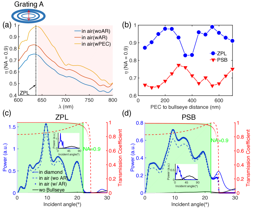
We first investigate for the collection efficiency of the NV ZPL into an NA of 0.9, which corresponds to a maximum collection angle of 21.9∘ in diamond. We optimize the circular grating structure to maximize (=637 nm, NA0=0.9), assuming the NV electric dipole is perpendicular to the diamond-air interface. This is a nonideal dipole orientation for efficient fluorescence collection, since most of the emission is at high modes which are difficult to collect efficiently. We choose this dipole orientation to demonstrate the effectiveness of the bullseye grating. The optimized circular grating (Grating A) achieves collection efficiency =75.2% , corresponding to a 210 fold enhancement from the baseline value of =0.36% . For comparison, the power emitted into the same collection window within diamond reaches 83.1% of the total emission power. The difference in is due to the nonunity Fresnel transmission coefficient (average 80%) of the bottom diamond-air surface. With an anti-reflection (AR) coating layer of index and thickness = nm on the bottom diamond surface, the averaged transmission for the bottom interface increases to 99% while increases to 83.0% .
The enhancement in collection efficiency is from the modification of far-field radiation profile to minimize . Fig.1(c) inset shows the simulated far-field pattern projected to air for Grating A with AR coating. Note that both the dipole emitter and the grating, and the resulting far-field pattern, have the same circular symmetry. The mode in Bullseye A is p polarized because the vertically polarized dipole source has only p polarized emission. The angular power distribution of polarization component for Grating A with AR coating (Fig.2(c)) indicates that bullseye structure effectively converts the nondirectional dipole emission (black solid line) into the collection window (plot in blue lines). Additionally, the AR coating improves the collection efficiency by maximizing the bottom interface transmission (plot in red lines) from an average value of 80% to 99%.
Lastly, the collection efficiency can be further improved by placing a reflector over the grating to minimize . The reflector could consist of an NSOM tip or silver coated fiber facet with piezo controlled stage 27. We find that when the reflector is 550 nm over the diamond surface, the collection reaches 98.9% . We assumed here a perfect reflector, modeled as perfect electric conductor in the simulation. The yellow line in Fig.2(a) shows the spectrally resolved collection efficiency for this reflector position.
We also evaluate the collection efficiency over the PSB with Grating A. We plot the power angular dependence for weighted averaged PSB emission in Fig.2(d) and found similar enhancement with an AR coating layer. We also simulated with PEC reflector over the grating for PSB case, which is shown in Fig.2(b), indicating that the optimal distance for PSB collection is 300 nm with (NA0=0.9, =640-800 nm) = 77.3% .
Grating B for scheme (c)
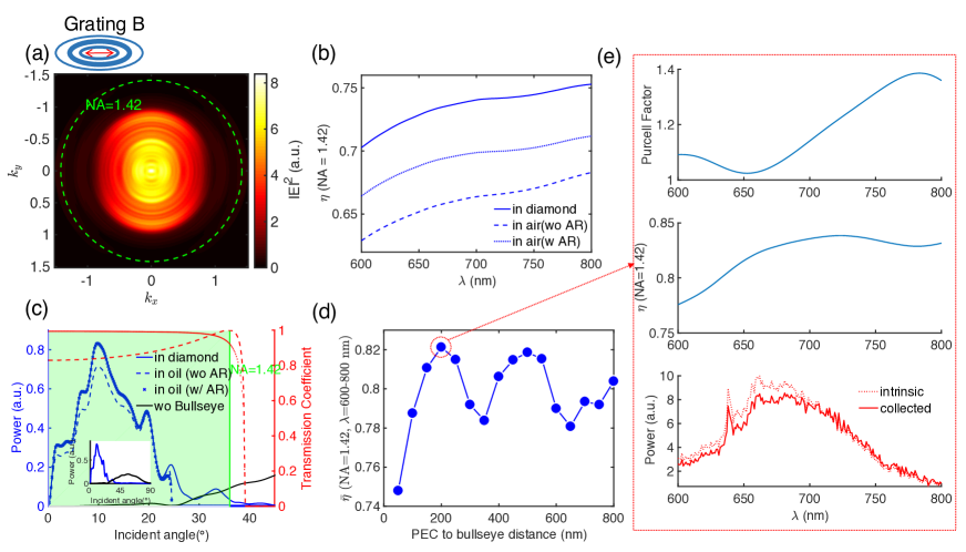
For many quantum sensing applications, efficient collection over the whole NV spectrum is required. These experiments are performed at room temperature with high-NA oil immersion objectives. Here we set the FOM of the optimization to be the collection efficiency weighted by the NV emission spectrum and averaged over the range = 600–800 nm. This we denote as (NA0=1.42, =600-800 nm) = NA0, where is the normalized power spectral density of NV emission. We also assume the collection medium is n=1.518 oil and a horizontal dipole configuration, which corresponds to a NV in a (111) terminated diamond film.
The performance of the optimized grating design (Grating B) is shown in Fig.3. The far-field emission pattern shown in Fig.3(a) indicates that the broadband emission can be largely captured by a lens with an NA of 1.42. The unweighted collection efficiency within this NA is plotted as a function of wavelength in Fig.3(b), illustrating the broadband performance of this design. The wavelength-averaged weighted collection efficiency for this grating is = 65.9% , which is increased to = 69.4% when a thin-film AR coating optimized for 662 nm is added to the diamond-oil interface. For comparison, the average weighted power emitted within the same NA in diamond is = 73.45%. The benefit of the AR coating is further illustrated by comparing the angular distribution of the emitted power without [Fig.3(c), dashed line] and with [Fig.3(c), crosses] the AR coating. The collected power is enhanced over a large angular range ( 0–24∘) and brought close to the intrinsic power measured in the diamond.
To further increase the collection efficiency by minimizing the power lost in the upwards direction, a PEC mirror is placed over the grating. As indicated in Fig.3(d), the optimal position of the mirror is 200 nm above the grating, which results in an averaged weighted collection efficiency of =82.2% , corresponding to a 6.5-fold enhancement relative to an NV in an unpatterned diamond film.
To verify that the optimized design is tailored for the input NV emission spectrum, we plot in Fig.3(e) the Purcell factor and collection efficiency over 600-800 nm range. Better performance is seen in the wavelength range where NVs emission is stronger. Note that the Purcell factor lies within the optimal range for maximal SNR.24 The results show the advantage of the chirped circular grating for broadband operation, compared to conventional gratings40.
We also compare the intrinsic NV emission spectrum (indicated by the dotted red line, measured experimentally) with the predicted collected power (emission spectrum collection efficiency Purcell factor, solid red line), indicating that near-unity photon collection is possible with these gratings.
Tolerance of the chirped circular gratings to NV displacement
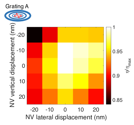
It is also important to consider the robustness of grating performance against the NV displacement from the grating center. The NV placement uncertainty for Nitrogen ion implantation is estimated from the statistical displacement range given by The Stopping and Range of Ions in Matter (SRIM) simulation 52. For an NV depth of 100 nm, the lateral and longitudinal displacements are both 20 nm. We calculate the collection efficiency of Grating A (under the same conditions as scheme (a), without AR coating or PEC mirror) as a function of NV displacement. Here the emitter is modeled as NV with both along the [01] direction and along [2] (a pair of dipoles whose contributions are summed incoherently, see Supporting Information S2 for the emission dipole orientations. This case is as also discussed by Sage et al. 22). The results in Fig.4 show the versus the displacement in lateral and longitudinal directions, with being the collection efficiency for zero displacement. The results indicate that the collection efficiency for Grating A is within 15.9% of under 20 nm of NV displacement. Such alignment accuracy can be achieved using the self-aligned ion implantation technique53, 54.
Conclusions
We proposed and numerically optimized chirped circular grating structures for near unity collection of NV fluorescence. The grating design is compatible with fabrication on a bulk diamond surface. Using an objective lens with an NA of 0.9, we show collection efficiency of 98.9% for NV ZPL emission, and averaged collection efficiency of 77.3% over the PSB range. For collection over 600 - 800 nm, we obtain weighted-averaged collection efficiency of 82.2% into NA of 1.42 oil objective and moderate averaged Purcell factor of 1.18. The detailed results are summarized in Table 1. For the emitter-grating alignment, the collection efficiency varies 15.9% for displacements within 20 nm from the center. Our approach is also applicable to emitters such as quantum dots or other solid state defects.
The narrow emission angle of the chirped grating could also allow efficient coupling into high-NA single-mode fibers55.
Furthermore, a dual grating-lens design where a second grating is added on the backside of the diamond film, can efficiently collimate the emission to certain target optical modes. Alternatively, a flat metasurface lens 56 could be positioned on the diamond backside for efficient interfacing to corresponding photonic structures.
Such grating structures can be fabricated using transferred hard mask lithography57, or direct fabrication on the diamond using electron beam lithography or optical lithography58.
Discussion on the intrinsic NV- emission rate, dipolar component orientations of NV, estimation of baseline collection efficiency values for dipole near diamond surface, further simulation comparison with other structures, and limitations of grating depth are shown in Supporting Information.
This research used resources of the Center for Functional Nanomaterials, which is a U.S. DOE Office of Science User Facility, at Brookhaven National Laboratory under Contract No. DE-SC0012704. The authors thank Tim Schröder, Noel Wan and Matthew Trusheim for valuable discussions. J.Z. acknowledges partial support from the Office of Naval Research (N00014-13-1-0316). E.H.C. was supported by the NASA Office of the Chief Technologist’s Space Technology Research Fellowship. D.E. acknowledges partial support from the NSF program EFRI ACQUIRE:“Scalable Quantum Communications with Error-Corrected Semiconductor Qubit” and the AFOSR Optimal Measurements for Scalable Quantum Technologies MURI.
References
- Nickerson et al. 2014 Nickerson, N. H.; Fitzsimons, J. F.; Benjamin, S. C. Freely Scalable Quantum Technologies Using Cells of 5-to-50 Qubits with Very Lossy and Noisy Photonic Links. Phys. Rev. X 2014, 4, 041041
- Nemoto et al. 2014 Nemoto, K.; Trupke, M.; Devitt, S. J.; Stephens, A. M.; Scharfenberger, B.; Buczak, K.; Nöbauer, T.; Everitt, M. S.; Schmiedmayer, J.; Munro, W. J. Photonic Architecture for Scalable Quantum Information Processing in Diamond. Phys. Rev. X 2014, 4, 031022
- Hensen et al. 2015 Hensen, B. et al. Loophole-free Bell inequality violation using electron spins separated by 1.3 kilometres. Nature 2015, 526, 682–686
- Ju et al. 2014 Ju, C.; Lei, C.; Xu, X.; Culcer, D.; Zhang, Z.; Du, J. NV-center-based digital quantum simulation of a quantum phase transition in topological insulators. Physical Review B 2014, 89, 045432
- Cramer et al. 2016 Cramer, J.; Kalb, N.; Rol, M. A.; Hensen, B.; Blok, M. S.; Markham, M.; Twitchen, D. J.; Hanson, R.; Taminiau, T. H. Repeated quantum error correction on a continuously encoded qubit by real-time feedback. Nature communications 2016, 7
- Neumann et al. 2013 Neumann, P.; Jakobi, I.; Dolde, F.; Burk, C.; Reuter, R.; Waldherr, G.; Honert, J.; Wolf, T.; Brunner, A.; Shim, J. H.; Suter, D.; Sumiya, H.; Isoya, J.; Wrachtrup, J. High-Precision Nanoscale Temperature Sensing Using Single Defects in Diamond. Nano Letters 2013, 13, 2738–2742, PMID: 23721106
- Degen et al. 2016 Degen, C.; Reinhard, F.; Cappellaro, P. Quantum sensing. arXiv preprint arXiv:1611.02427 2016,
- Laraoui et al. 2015 Laraoui, A.; Aycock-Rizzo, H.; Gao, Y.; Lu, X.; Riedo, E.; Meriles, C. A. Imaging thermal conductivity with nanoscale resolution using a scanning spin probe. Nature communications 2015, 6
- Pingault et al. 2017 Pingault, B.; Jarausch, D.-D.; Hepp, C.; Klintberg, L.; Becker, J. N.; Markham, M.; Becher, C.; Atatüre, M. Coherent control of the silicon-vacancy spin in diamond. Nat. Commun. 2017, 8, 15579
- Neu et al. 2011 Neu, E.; Fischer, M.; Gsell, S.; Schreck, M.; Becher, C. Fluorescence and polarization spectroscopy of single silicon vacancy centers in heteroepitaxial nanodiamonds on iridium. Physical Review B 2011, 84, 205211
- Müller et al. 2014 Müller, T.; Hepp, C.; Pingault, B.; Neu, E.; Gsell, S.; Schreck, M.; Sternschulte, H.; Steinmüller-Nethl, D.; Becher, C.; Atatüre, M. Optical signatures of silicon-vacancy spins in diamond. Nature communications 2014, 5
- Hepp et al. 2014 Hepp, C.; Müller, T.; Waselowski, V.; Becker, J. N.; Pingault, B.; Sternschulte, H.; Steinmüller-Nethl, D.; Gali, A.; Maze, J. R.; Atatüre, M.; Becher, C. Electronic Structure of the Silicon Vacancy Color Center in Diamond. Phys. Rev. Lett. 2014, 112, 036405
- Pingault et al. 2014 Pingault, B.; Becker, J. N.; Schulte, C. H. H.; Arend, C.; Hepp, C.; Godde, T.; Tartakovskii, A. I.; Markham, M.; Becher, C.; Atatüre, M. All-Optical Formation of Coherent Dark States of Silicon-Vacancy Spins in Diamond. Phys. Rev. Lett. 2014, 113, 263601
- Gaebel et al. 2004 Gaebel, T.; Popa, I.; Gruber, A.; Domhan, M.; Jelezko, F.; Wrachtrup, J. Stable single-photon source in the near infrared. New Journal of Physics 2004, 6, 98
- Iwasaki et al. 2015 Iwasaki, T. et al. Germanium-Vacancy Single Color Centers in Diamond. Sci. Rep. 2015, 5, 12882
- Aharonovich et al. 2010 Aharonovich, I.; Castelletto, S.; Simpson, D. A.; Greentree, A. D.; Prawer, S. Photophysics of chromium-related diamond single-photon emitters. Physical Review A 2010, 81, 043813
- Widmann et al. 2015 Widmann, M. et al. Coherent control of single spins in silicon carbide at room temperature. Nat. Mater. 2015, 14, 164–168
- Taylor et al. 2008 Taylor, J.; Cappellaro, P.; Childress, L.; Jiang, L.; Budker, D.; Hemmer, P.; Yacoby, A.; Walsworth, R.; Lukin, M. High-sensitivity diamond magnetometer with nanoscale resolution. Nature Physics 2008, 4, 810–816
- Budker and Romalis 2007 Budker, D.; Romalis, M. Optical magnetometry. Nat Phys 2007, 3, 227–234
- Hong et al. 2013 Hong, S.; Grinolds, M. S.; Pham, L. M.; Sage, D. L.; Luan, L.; Walsworth, R. L.; Yacoby, A. Nanoscale magnetometry with NV centers in diamond. MRS Bulletin 2013, 38, 155–161
- Epstein et al. 2005 Epstein, R.; Mendoza, F.; Kato, Y.; Awschalom, D. Anisotropic interactions of a single spin and dark-spin spectroscopy in diamond. Nature physics 2005, 1, 94–98
- Le Sage et al. 2012 Le Sage, D.; Pham, L. M.; Bar-Gill, N.; Belthangady, C.; Lukin, M. D.; Yacoby, A.; Walsworth, R. L. Efficient photon detection from color centers in a diamond optical waveguide. Phys. Rev. B 2012, 85, 121202
- Doherty et al. 2013 Doherty, M. W.; Manson, N. B.; Delaney, P.; Jelezko, F.; Wrachtrup, J.; Hollenberg, L. C. L. The nitrogen-vacancy colour centre in diamond. Phys. Rep. 2013, 528, 1–45
- Wolf et al. 2015 Wolf, S. A.; Rosenberg, I.; Rapaport, R.; Bar-Gill, N. Purcell-enhanced optical spin readout of nitrogen-vacancy centers in diamond. Phys. Rev. B 2015, 92, 235410
- Bogdanov et al. 2017 Bogdanov, S.; Shalaginov, M. Y.; Akimov, A.; Lagutchev, A. S.; Kapitanova, P.; Liu, J.; Woods, D.; Ferrera, M.; Belov, P.; Irudayaraj, J.; Boltasseva, A.; Shalaev, V. M. Electron spin contrast of Purcell-enhanced nitrogen-vacancy ensembles in nanodiamonds. arXiv: 1703.06991 2017,
- Patel et al. 2016 Patel, R. N.; Schröder, T.; Wan, N.; Li, L.; Mouradian, S. L.; Chen, E. H.; Englund, D. R. Efficient photon coupling from a diamond nitrogen vacancy center by integration with silica fiber. Light: Science & Applications 2016, 5, e16032
- Israelsen et al. 2014 Israelsen, N. M.; Kumar, S.; Tawfieq, M.; Neergaard-Nielsen, J. S.; Huck, A.; Andersen, U. L. Increasing the photon collection rate from a single NV center with a silver mirror. Journal of Optics 2014, 16, 114017
- Marseglia et al. 2011 Marseglia, L.; Hadden, J. P.; Stanley-Clarke, A. C.; Harrison, J. P.; Patton, B.; Ho, Y.-L. D.; Naydenov, B.; Jelezko, F.; Meijer, J.; Dolan, P. R.; Smith, J. M.; Rarity, J. G.; O’Brien, J. L. Nanofabricated solid immersion lenses registered to single emitters in diamond. Applied Physics Letters 2011, 98, 133107
- Hadden et al. 2010 Hadden, J.; Harrison, J.; Stanley-Clarke, A.; Marseglia, L.; Ho, Y.-L.; Patton, B.; O’Brien, J.; Rarity, J. Strongly enhanced photon collection from diamond defect centers under microfabricated integrated solid immersion lenses. Applied Physics Letters 2010, 97, 241901
- Schell et al. 2014 Schell, A. W.; Neumer, T.; Shi, Q.; Kaschke, J.; Fischer, J.; Wegener, M.; Benson, O. Laser-written parabolic micro-antennas for efficient photon collection. Applied Physics Letters 2014, 105
- Babinec et al. 2010 Babinec, T. M.; Hausmann, B. J.; Khan, M.; Zhang, Y.; Maze, J. R.; Hemmer, P. R.; Lončar, M. A diamond nanowire single-photon source. Nature nanotechnology 2010, 5, 195–199
- Riedel et al. 2014 Riedel, D.; Rohner, D.; Ganzhorn, M.; Kaldewey, T.; Appel, P.; Neu, E.; Warburton, R.; Maletinsky, P. Low-loss broadband antenna for efficient photon collection from a coherent spin in diamond. Physical Review Applied 2014, 2, 064011
- Momenzadeh et al. 2015 Momenzadeh, S. A.; Stöhr, R. J.; de Oliveira, F. F.; Brunner, A.; Denisenko, A.; Yang, S.; Reinhard, F.; Wrachtrup, J. Nanoengineered Diamond Waveguide as a Robust Bright Platform for Nanomagnetometry Using Shallow Nitrogen Vacancy Centers. Nano Letters 2015, 15, 165–169, PMID: 25438091
- Choy et al. 2011 Choy, J. T.; Hausmann, B. J.; Babinec, T. M.; Bulu, I.; Khan, M.; Maletinsky, P.; Yacoby, A.; Lončar, M. Enhanced single-photon emission from a diamond-silver aperture. Nature Photonics 2011, 5, 738–743
- Choy et al. 2013 Choy, J. T.; Bulu, I.; Hausmann, B. J. M.; Janitz, E.; Huang, I.-C.; Lončar, M. Spontaneous emission and collection efficiency enhancement of single emitters in diamond via plasmonic cavities and gratings. Applied Physics Letters 2013, 103, 161101
- Scheuer et al. 2006 Scheuer, J.; Green, W. M.; Yariv, A. Annular Bragg resonators (ABR): the ideal tool for biochemical sensing, nonlinear optics, and cavity QED. Integrated Optoelectronic Devices 2006. 2006; pp 61230S–61230S
- Scheuer and Yariv 2004 Scheuer, J.; Yariv, A. Circular photonic crystal resonators. Phys. Rev. E 2004, 70, 036603
- Davanço et al. 2011 Davanço, M.; Rakher, M.; Schuh, D.; Badolato, A.; Srinivasan, K. A circular dielectric grating for vertical extraction of single quantum dot emission. Applied Physics Letters 2011, 99, 041102
- Ateş et al. 2012 Ateş, S.; Sapienza, L.; Davanço, M.; Badolato, A.; Srinivasan, K. Bright Single-Photon Emission From a Quantum Dot in a Circular Bragg Grating Microcavity. Selected Topics in Quantum Electronics, IEEE Journal of 2012, 18, 1711–1721
- Li et al. 2015 Li, L.; Chen, E. H.; Zheng, J.; Mouradian, S. L.; Dolde, F.; Schröder, T.; Karaveli, S.; Markham, M. L.; Twitchen, D. J.; Englund, D. Efficient Photon Collection from a Nitrogen Vacancy Center in a Circular Bullseye Grating. Nano Letters 2015, 15, 1493–1497, PMID: 25714414
- Kärtner et al. 1997 Kärtner, F. X.; Matuschek, N.; Schibli, T.; Keller, U.; Haus, H. A.; Heine, C.; Morf, R.; Scheuer, V.; Tilsch, M.; Tschudi, T. Design and fabrication of double-chirped mirrors. Optics letters 1997, 22, 831–833
- Agrawal and Peumans 2008 Agrawal, M.; Peumans, P. Broadband optical absorption enhancement through coherent light trapping in thin-film photovoltaic cells. Opt. Express 2008, 16, 5385–5396
- Zheng et al. 2014 Zheng, J.; Barton, R. A.; Englund, D. Broadband Coherent Absorption in Chirped-Planar-Dielectric Cavities for 2D-Material-Based Photovoltaics and Photodetectors. ACS Photonics 2014, 1, 768–774
- Lee et al. 2011 Lee, K.; Chen, X.; Eghlidi, H.; Kukura, P.; Lettow, R.; Renn, A.; Sandoghdar, V.; Götzinger, S. A planar dielectric antenna for directional single-photon emission and near-unity collection efficiency. Nat Photon 2011, 5, 166–169
- Hodges et al. 2012 Hodges, J. S.; Li, L.; Lu, M.; Chen, E. H.; Trusheim, M. E.; Allegri, S.; Yao, X.; Gaathon, O.; Bakhru, H.; Englund, D. Long-lived NV − spin coherence in high-purity diamond membranes. New Journal of Physics 2012, 14, 093004
- Piracha et al. 2016 Piracha, A. H.; Rath, P.; Ganesan, K.; Kühn, S.; Pernice, W. H. P.; Prawer, S. Scalable Fabrication of Integrated Nanophotonic Circuits on Arrays of Thin Single Crystal Diamond Membrane Windows. Nano Letters 2016, 16, 3341–3347, PMID: 27111636
- Jung et al. 2016 Jung, T.; Kreiner, L.; Pauly, C.; Mücklich, F.; Edmonds, A. M.; Markham, M.; Becher, C. Reproducible fabrication and characterization of diamond membranes for photonic crystal cavities. Phys. Status Solidi 2016, 213, 3254–3264
- Schröder et al. 2017 Schröder, T.; Trusheim, M. E.; Walsh, M.; Li, L.; Zheng, J.; Schukraft, M.; Sipahigil, A.; Evans, R. E.; Sukachev, D. D.; Nguyen, C. T.; Pacheco, J. L.; Camacho, R. M.; Bielejec, E. S.; Lukin, M. D.; Englund, D. Scalable focused ion beam creation of nearly lifetime-limited single quantum emitters in diamond nanostructures. Nat. Commun. 2017, 8, 15376
- Novotny and Hecht 2012 Novotny, L.; Hecht, B. Principles of nano-optics; Cambridge university press, 2012
- Chu et al. 2014 Chu, Y. et al. Coherent Optical Transitions in Implanted Nitrogen Vacancy Centers. Nano Letters 2014, 14, 1982–1986, PMID: 24588353
- Ofori-Okai et al. 2012 Ofori-Okai, B. K.; Pezzagna, S.; Chang, K.; Loretz, M.; Schirhagl, R.; Tao, Y.; Moores, B. A.; Groot-Berning, K.; Meijer, J.; Degen, C. L. Spin properties of very shallow nitrogen vacancy defects in diamond. Physical Review B 2012, 86, 081406
- Ziegler et al. 2010 Ziegler, J. F.; Ziegler, M.; Biersack, J. {SRIM} – The stopping and range of ions in matter (2010). Nuclear Instruments and Methods in Physics Research Section B: Beam Interactions with Materials and Atoms 2010, 268, 1818 – 1823, 19th International Conference on Ion Beam Analysis
- Schukraft et al. 2016 Schukraft, M.; Zheng, J.; Schröder, T.; Mouradian, S. L.; Walsh, M.; Trusheim, M. E.; Bakhru, H.; Englund, D. R. Invited Article: Precision nanoimplantation of nitrogen vacancy centers into diamond photonic crystal cavities and waveguides. APL Photonics 2016, 1, 020801
- Schröder et al. 2017 Schröder, T.; Walsh, M.; Zheng, J.; Mouradian, S.; Li, L.; Malladi, G.; Bakhru, H.; Lu, M.; Stein, A.; Heuck, M.; Englund, D. Scalable fabrication of coupled NV center - photonic crystal cavity systems by self-aligned N ion implantation. Opt. Mater. Express, OME 2017, 7, 1514–1524
- Preble et al. 2015 Preble, S. F.; Fanto, M. L.; Steidle, J. A.; Tison, C. C.; Howland, G. A.; Wang, Z.; Alsing, P. M. On-Chip Quantum Interference from a Single Silicon Ring-Resonator Source. Phys. Rev. Applied 2015, 4, 021001
- Yu et al. 2011 Yu, N.; Genevet, P.; Kats, M. A.; Aieta, F.; Tetienne, J.-P.; Capasso, F.; Gaburro, Z. Light Propagation with Phase Discontinuities: Generalized Laws of Reflection and Refraction. Science 2011, 334, 333–337
- Li et al. 2015 Li, L.; Bayn, I.; Lu, M.; Nam, C.-Y.; Schröder, T.; Stein, A.; Harris, N. C.; Englund, D. Nanofabrication on unconventional substrates using transferred hard masks. Scientific reports 2015, 5
- Schröder et al. 2016 Schröder, T.; Mouradian, S. L.; Zheng, J.; Trusheim, M. E.; Walsh, M.; Chen, E. H.; Li, L.; Bayn, I.; Englund, D. Quantum nanophotonics in diamond [Invited]. J. Opt. Soc. Am. B, JOSAB 2016, 33, B65–B83