Real-space study of the optical absorption in alternative phases of silicon
Abstract
We introduce a real-space approach to understand the relationship between optical absorption and crystal structure. We apply this approach to alternative phases of silicon, with a focus on the Si20 crystal phase as a case study. We find that about 83% of the changes in the calculated low-energy absorption in Si20 as compared to Si in the diamond structure can be attributed to reducing the differences between the on-site energies of the bonding and anti-bonding orbitals as well as increasing the hopping integrals for specific Si-Si bonds.
I Introduction
In order to reduce the cost of solar-cell energy generation, a great deal of effort has been put into attempts to increase the number of charge carriers collected by the solar cell relative to the number of incident photons (quantum efficiency). Silicon is the most widely used photovoltaic material. In terms of global annual power production, a recent market survey shows that crystalline silicon dominates the photovoltaic industry 90%. One of the major reasons for its popularity is that silicon is non-toxic and abundant. There are also benefits from technologies developed over the years in the microelectronics industry.
Despite its widespread usage as a photovoltaic material, silicon does not efficiently absorb most of the light in the solar spectrum. The solar spectrum that is received at the Earth’s surface (under the so-called air mass of 1.5 or AM 1.5 for shortast ) ranges from 0.3 eV to 4.4 eV and is the strongest around 1.2 eV. Since silicon has a direct band gap of 3.3 eV, optical absorption due to direct transitions can only take place at the high-energy end of the solar spectrum between 3.3 and 4.4 eV. Phonon-assisted indirect transitionsNoffsinger et al. (2012); Macfarlane et al. (1958) lower the onset of optical absorption to 1.2 eV. Even then, absorption coefficients due to indirect transitions alone are smaller and require the solar cell to be thick in order to amplify the phonon contributions. With a thicker absorber layer, the solar cell has to have high purity to prolong its carriers lifetime. Together, the increased thickness and need for material purity add to the cost of production.
Under ambient conditions, the diamond cubic phase (diamond-Si) is the most stable crystal phase of silicon, and this is also the crystal phase of silicon most commonly used to make solar cells today. However, silicon is known to exist in other crystal phases as well. For instance, with increase in pressure, silicon undergoes phase transitions from the diamond-Si phase to the -Sn phase,Jamieson (1963) Imma phaseMcMahon et al. (1994), simple hexagonal phase Olijnyk et al. (1984); Hu and Spain (1984); Chang and Cohen (1984); Chang et al. (1985) and Cmca phaseHanfland et al. (1999). Pressure release from the -Sn phase does not recover the diamond-Si phase. Instead, a slow pressure release produces the metastable R8 phasePiltz et al. (1995) which subsequently transforms into the BC8 phase,Minomura and Drickamer (1962); Kasper and Richards (1964); Wentorf and Kasper (1963); Malone et al. (2008a) while a very rapid pressure release leads to two other tetragonal phases.Zhao et al. (1986) Many of these phases are not suitable to make solar cells. For example, the first four phases mentioned above only exist under high pressure. The -Sn and simple hexagonal phases are also metallicChang and Cohen (1984); Chang et al. (1985) while the BC8 phaseMalone et al. (2008a) is semi-metallic. On the other hand, phases like the R8Malone et al. (2008b) and body-centered tetragonalMalone et al. (2010) phases are semiconducting, and since they have direct band gaps smaller than diamond-Si’s, they in principle can also absorb light over a wider energy rangeCohen and Malone (2011) than diamond-Si.
One approachCohen and Malone (2011) to increasing the absorption range of silicon is then to find a crystal phase of silicon that has a smaller direct band gap than that of diamond-Si. With the advent of first-principles computational techniques, it has become possible to searchWang et al. (2010); Cerqueira et al. (2015); Pickard and Needs (2006); Lee et al. (2016) for crystal phases that have not been previously discovered. Botti et al. Botti et al. (2012) found several crystal phases of silicon that have lower energies than the R8 and BC8 phases and have quasiparticle band gaps ranging from 0.8 to 1.5 eV from GW calculations. Wang et al. Wang et al. (2014) proposed phases of silicon that have band gaps from 0.39 to 1.25 eV obtained within density functional theory (DFT) using the hybrid HSE functional. Focusing on silicon with direct gaps, Lee et al. Lee et al. (2014) presented several other silicon phases.
Recently, Xiang et al. in Ref. Xiang et al., 2013 found the structure of Si20 (also called Si20-T) using the particle swarm optimization (PSO)Wang et al. (2010) approach. Their calculated band gap of Si20 is 1.55 eV within DFT-HSE, which is close to the optimal gap (1.3–1.4 eV)Rühle (2016); Queisser (2009) for solar energy conversion according to the Shockley-Quiesser model.Shockley and Queisser (1961) One of the structural features of Si20, which is not found in diamond-Si, is that some of the bonds form equilateral triangles. In Ref. Xiang et al., 2013, it was suggested that these bonds might be related to its improved optical absorption. Nevertheless, the microscopic reason for the increase in the calculated absorption in Si20 remained unknown. In a related work, Guo et al. in Ref. Guo et al., 2015 proposed an alternative ground state of silicon with a band gap of 0.61 eV from DFT-HSE that also contains triangular bonds.
The purpose of this work is to understand how the structure of an alternative silicon phase may lead to an improved calculated absorption relative to diamond-Si. While there are many proposed metastable phases of silicon with improved absorption, we focus here on Si20 as a case study for our approach since Si20 has a desired calculated optical absorption. (We also note that Si20 has a somewhat high formation energy,Lee et al. (2014); Amsler et al. (2014); Xiang et al. (2014) which may make it harder to access experimentally.)
One of the obstacles in establishing the relationship between the crystal structure and optical absorption is the fact that the crystal structures of Si20 and diamond-Si are very different. For example, one cannot be related to the other by the removal or addition of a single atom, or by a small structural distortion that will not drastically disturb the bonding network of the silicon atoms. Moreover, the primitive unit cell of diamond-Si contains two atoms whereas that of Si20 contains 20 atoms. Therefore, a conventional analysis of optical absorption in the reciprocal space is non-trivial as each k-point in Si20 contains 40 valence and 40 conduction -like bands (unlike diamond-Si, which only has four of each).
To overcome this difficulty, we study the optical absorption in a real space representation. Our real space analysis reveals that about 33% of the enhanced optical absorption of Si20 can be attributed to the decreased differences of the on-site energies between the bonding and anti-bonding orbitals. Roughly 50% is due to the increased hopping integrals between the bonding and anti-bonding orbitals. The remaining 17% is due to a variety of other contributions.
II Method
In this section, we will first describe the conventional density functional theory (DFT) interband-transition approach and the GW plus Bethe-Salpeter equation (GW-BSE) approach for computing optical absorption in reciprocal space. The latter approach includes electron self-energy and electron-hole (excitonic) effects. Next we briefly introduce a real-space representation of the electronic structure in terms of Wannier functions. Finally, we transform the expression for the optical absorption from the reciprocal space representation into the real space representation.
II.1 Optical absorption
Optical absorption can be expressed through , the imaginary part of the dielectric function. Within the independent-particle DFT approach and neglecting the photon momentum, the diagonal elements of can be computed using the random-phase approximation for a specific light polarization,
| (1) | ||||
Here is the wave vector, is the polarization direction, is the position operator, is the frequency of absorbed photon, and are the DFT eigenvalues, and are the DFT Bloch eigenstates and and are the valence and conduction bands. The matrix element describes a transition of an electron from state into state upon the absorption of a photon.
The calculated within the DFT approach is shown in Fig. 1a for diamond-Si (black) and Si20 (red). In this calculation we used a norm-conserving pseudopotential and we used the local density approximation as implemented in Quantum-ESPRESSO.Giannozzi et al. (2009) The plane-wave cutoff for the electron wavefunction is 36 Ry. For diamond-Si, the Wannier functions are constructed from a coarse k-mesh of and they are used to interpolate quantities on a fine k-mesh of to calculate . For Si20, the coarse k-mesh is and the fine k-mesh is .
From Fig. 1a, it is clear that within the DFT approach, the onset of optical absorption in Si20 is 1.7 eV lower in energy than in diamond-Si. However, absorption of Si20 at the absorption edge is relatively small, and it increases significantly only at 0.8 eV above the absorption edge. Comparing the steep edges of the absorption spectra, the steep edge of Si20 is still about 0.9 eV lower in energy than it is for diamond-Si.
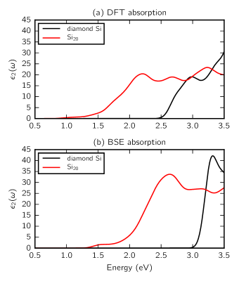
In what follows, we discuss two well-known limitations of the optical absorption calculated within the DFT-RPA approach. The first limitation is that the calculated DFT-LDA band gap is typically too small due the fact that DFT eigenvalues are not quasiparticle excitation energies. The GW approximationHybertsen and Louie (1986) removes this limitation by properly including the electron self energy effects. In the case of Si20 and diamond-Si, the inclusion of the GW correctiontob separates the DFT valence and conduction bands by 0.7–0.8 eV (depending on the k-points and electron bands) which is close to the value obtained by the hybrid-functional approach in Ref. Xiang et al., 2013.
The second limitation of the optical absorption calculated within the DFT approach is that it does not consider electron-hole interactions. Within the interacting many-electron picture, an electron is excited from a ground state to an excited excitonic state in which the electron interacts with the hole that it left behind. This process can be calculatedRohlfing and Louie (2000) by solving the BSE and is then expressed as,
| (2) |
Here S labels the exciton states and is the exciton eigenenergy.
The spectra calculatedtob by solving the BSE for Si20 and diamond-Si are shown in Fig. 1b. Comparing the GW-BSE and DFT absorption spectra, we see two main differences. First, the absorption edge in the GW-BSE spectrum is 0.6 eV higher in energy than the edge in the DFT spectrum. This shift is close to the shift resulting from the GW correction (0.7 eV). The second difference with the GW-BSE approach is that is larger in amplitude by a factor of about 1.5–2.0 near the band edge.
Therefore, while the optical absorption in absolute terms is very different between the GW-BSE and DFT approaches, the corrections made by the GW-BSE approach are nearly the same for both Si20 and diamond-Si. To better understand the improved absorption of Si20, it is sufficient to focus on an analysis of results from the DFT-RPA approach, since the geometric effect of the crystal structure is already present at the DFT-RPA level.
II.2 Localized representation
The Bloch states appearing in the expression for (in Eq. 1) have a well-defined crystal momentum . They are eigenstates of the Kohn-Sham Hamiltonian,
| (3) |
By superposing the Bloch states of different crystal momenta , one can construct a well localized Wannier state,
| (4) |
Here is a real-space lattice vector and is an arbitrary unitary matrix that mixes the Bloch bands at . In this paper, we use indices and to denote individual Wannier functions and indices and to denote individual Bloch bands.
One often chooses the matrices according to the scheme introduced by Marzari and VanderbiltMarzari and Vanderbilt (1997) so that is as localized in real space around the centers of mass of the Wannier functions as possible. For this reason, is also called the maximally localized Wannier function. The Bloch functions can be reconstructed back from the Wannier functions through an inverse transformation,
| (5) |
Since the set of Wannier functions contains the same amount of information as the set of Bloch bands from which it is generated, it is convenient to rewrite the Hamiltonian and position operators in the Wannier basis. The Hamiltonian in the Wannier (or real space) representation is simply which can be calculated by a Fourier transform of ,
| (6) |
There are two types of Hamiltonian matrix elements that we will focus on in this paper. For the first type, we have and . We will refer to this type of matrix element,
| (7) |
as the on-site energy of Wannier function . The remaining matrix elements
| (8) |
are known as the hopping integrals. The hopping integral measures the probability amplitude for Wannier function in cell to tunnel to the Wannier function in the unit cell at the origin.
Wannier functions are constructed from a set of Bloch bands so a different choice of Bloch bands will lead to different Wannier functions. Since the expression for optical absorption in Eq. 1 refers explicitly to occupied and empty Bloch states, we constructed the Wannier functions either from only empty or only occupied Bloch states. Therefore, by construction, is zero unless bra and ket are either both derived from empty or occupied states.
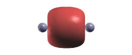
(a) Bonding Wannier function
(b) Anti-bonding Wannier function
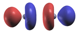
We will refer to the Wannier functions constructed from the occupied Bloch states as bonding Wannier functions and those from the empty states of the relevant conduction bands as anti-bonding Wannier functions since they typically have real-space forms that resemble bonding and anti-bonding molecular orbitals. Since silicon bonds are highly covalent, the valence charges are localized on the bonds between these two nearest-neighboring silicon atoms. Therefore, the bonding and anti-bonding Wannier states are localized in the region between these two silicon atoms, as shown in Fig. 2 for the case of diamond-Si. Each Si-Si bond has only one -like bonding and one -like anti-bonding Wannier function (per each spin). For convenience, we will label the on-site energy for the bonding and anti-bonding states as,
respectively. Similarly, we denote the hopping integral between anti-bonding states as .
II.3 Optical absorption in the localized basis
The optical absorption calculated using (Eq. 1) within the DFT-RPA approach depends on the energy of the Bloch states , and the matrix element of the position operator. The Bloch state energies are fully determined by and . Similarly, the position operator matrix element can be computed from its representation in the Wannier basis
| (9) |
In all, optical absorption is exactly determined given the following three real-space quantities: , , and .
III Results and discussion
In this section, we will compare , , and in diamond-Si and Si20 and relate them to the structural differences between the two materials, as well as the differences in their optical absorption.
III.1 Comparison of structures
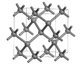
Figures 3 and 4 show the crystal structures of diamond-Si and Si20. Both of their conventional unit cells have cubic lattices. In our calculations, we use fully relaxed structures of Si20 and diamond-Si. The lattice parameters of the conventional unit cells of Si20 and diamond-Si are 7.40 Å and 5.43 Å. On the average, Si20 has one Si atom every 20.2 Å3 (2.30 g/cm3) and diamond-Si has one atom every 20.0 Å3 (2.33 g/cm3).
Each Si atom in diamond-Si is tetrahedrally coordinated to four other Si atoms, such that every bond angle is exactly 109.5∘. Every Si-Si bond in diamond-Si is symmetrically equivalent. The distance between the bond centers of two nearest-neighboring bonds is 1.9 Å.
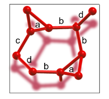
For Si20, every Si atom is also coordinated to four other Si, but in a distorted tetrahedron. The distortions bring some of the bond centers of Si20 closer together and others further apart. There are four symmetry-inequivalent groups of Si-Si bonds in Si20 and they are labelled from a to d in Fig. 4. One feature of the Si20 structure is the type-a bonds which form triangles. These bonds are highly strained as they are distorted from 109.5∘ to a narrow 60.0∘. As a result, the distance between two nearest-neighboring bond centers ranges from as short as 1.2 Å (between two type-a bonds of the same triangle) to 2.1 Å. We will label this range, 1.2–2.1 Å, as the nearest-neighbor hopping regime.
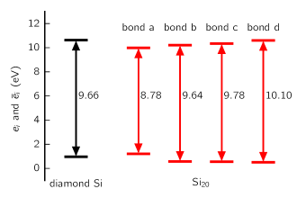
III.2 On-site energy
Here we compare on-site energies of diamond-Si and Si20. Since we can assign a single bonding and anti-bonding Wannier function to each Si-Si bond, we will focus here on comparing the on-site energies, and , for the same bond in the crystal.
Calculated values of and for diamond-Si and Si20 are shown in Fig. 5 with horizontal lines. The arrow represents the difference between and for a given set of symmetry-related bonds in the structure. In the case of diamond-Si, for its Si-Si bond is 9.66 eV. On the other hand, for Si20 ranges from 8.78 to 10.10 eV. The smallest value (8.78 eV) belongs to the highly strained type-a bonds. Its large deviation from diamond-Si’s 9.66 eV is likely because of its strain, due to the distortion from 109.5∘ to 60∘. Less strained type-b and type-c bonds have similar to that in diamond-Si (9.64 and 9.78 eV). Finally, type-d bonds have the largest ( eV).
We expect that the smaller of type-a bonds would lower the optical absorption edge of Si20 with respect to diamond-Si’s. This will be analyzed in more detail in Sec. III.5.
III.3 Hopping integral
After analyzing , we now focus on the hopping integral of diamond-Si and Si20.
For the analysis of , we will define the hopping distance as the distance between the centers of mass of the Wannier functions and ,
In what follows, we will relate with its hopping distance.
III.3.1 Bonding states
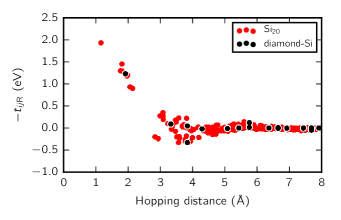
First, we discuss the hopping integrals between bonding Wannier functions. As shown in Fig. 6, the hopping integrals of both diamond-Si and Si20 are nearly zero for hopping distances beyond 5 Å. This behavior is characteristic of the exponential localizationBrouder et al. (2007) of Wannier functions for insulators.
The hopping integral with the largest magnitude for diamond-Si is eV. This hopping integral couples a bonding Wannier function with its nearest bonding neighbor and has a hopping distance of 1.9 Å. In Fig. 6, it is denoted by the leftmost black dot. For Si20, hopping integrals coupling the nearest bonding neighbors are distributed over the range of 1.2–2.1 Å (see Sec. III.1). In Fig. 6, they are represented by the group of red dots surrounding the above-mentioned black dot.
The largest for Si20 corresponds to the hopping integral with the shortest hopping distance of 1.2 Å. This hopping integral couples type-a bonds and is 0.70 eV larger than the largest of diamond-Si. The presence of this large hopping integral in Si20 is due to the fact that the distance between triangular bonds is Å shorter than the shortest bond–bond distance in diamond-Si.
As we will analyze later in more detail, we expect the larger hopping integrals of the occupied Wannier functions to raise the valence band edge in Si20 as we expect the valence bands to have a larger bandwidth.
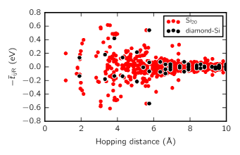
III.3.2 Anti-bonding states
Now, we look at the hopping integrals between the anti-bonding states. Figure 7 shows that the largest for diamond-Si is 0.54 eV and has a hopping distance of 5.8 Å. Unlike the bonding states, this largest does not couple the nearest-neighboring Wannier functions. That hopping integral is four times smaller (0.13 eV). For Si20, the largest is 0.62 eV and has a hopping distance of 3.5 Å. It is somewhat larger than diamond-Si’s largest and it also does not couple the nearest-neighboring Wannier functions.
Nevertheless, in the nearest-neighbor hopping regime of 1.2–2.1 Å, the largest in Si20 is 0.40 eV. This value is significantly larger than the corresponding for diamond-Si (0.13 eV) in the same regime.
Notably, even though for anti-bonding Wannier functions are nearly zero above hopping distance of 9 Å, it does not increase monotonically below 9 Å as the hopping distance decreases. The distribution of (Fig. 7) is more dispersive than that of (Fig. 6). This is likely related to the fact that the anti-bonding Wannier functions (Fig. 2b) have more nodes than the bonding Wannier functions (Fig. 2a). They are also more diffuse than the bonding Wannier functions. In addition, anti-bonding Wannier functions hybridize with the continuum, making them somewhat sensitive to the choice of the frozen window used in the Wannier disentanglementSouza et al. (2001) procedure. (For consistency, we have chosen the frozen windows in both diamond-Si and Si20 to span from the conduction band minimum (CBM) to 3.7 eV above the CBM.)
Hopping integrals between anti-bonding Wannier states of Si20 are distributed over a wider energy range than diamond-Si. We expect the larger hopping integrals between the empty Wannier functions of Si20 to increase the bandwidth of the conduction bands and lower its lower band edge. This will be further discussed in Sec. III.5.
III.4 Position integral
Now we discuss the third real-space object required to compute the optical absorption: position operator in the real space representation, , between a bonding Wannier function and an anti-bonding Wannier function. (The matrix elements between two bonding or two anti-bonding Wannier functions do not enter into Eq. (1).)
For diamond-Si, is the largest when and are both centered on the same bond, as can be expected. Its value is Å2 and it is seven times as large than that between the neighboring bonds (0.09 Å2). For Si20, the largest are also on the same bond. Their values for four types of Si20 bonds are nearly the same. Their average value is 0.530.02 Å2. (The next largest value is only 0.15 Å2.)
Here, two observations can be made. First, we see that in the real space representation, , like the Hamiltonian, is highly localized. Second, the largest for Si20 and diamond-Si have nearly the same numerical value. This is likely because the Wannier functions of Si20 have similar real-space character as those in diamond-Si.
III.5 Relating and to the optical absorption
Now, we will relate the magnitudes of and to the optical absorption in diamond-Si and Si20. For this purpose, we compute the optical absorption in three model systems, which are hybrids between diamond-Si and Si20. These hybrid systems have the same Hamiltonian as Si20, except for some , , and which are modified to resemble those in diamond-Si. Figure 8 shows the calculated optical spectra of diamond-Si (in solid black), Si20 (in solid red), and the hybrid systems (in dashed, dotted-and-dashed, and dotted red).
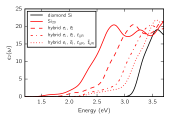
The dashed red curve in Fig. 8 shows the calculated optical absorption of the first hybrid system, where all on-site energies, and , of Si20 are made to be equal to those of diamond-Si.
The dotted-and-dashed curve in Fig. 8 represents the second hybrid system where, on top of the modifications made for the first hybrid system, hopping integrals between bonding Wannier functions are modified as well. This modification is done in the following way. First, we identify hopping integrals in Si20 larger than the nearest-neighbor hopping integral in diamond-Si (their values are , , , and eV). Second, we modify these hopping integrals so that they are equal to the nearest-neighbor hopping integral in the diamond-Si ( eV).
Finally, the dotted red curve in Fig. 8 shows the optical absorption of the third hybrid system which, in addition to the modifications made for the first and second hybrid system, has modified hopping integrals between the anti-bonding Wannier functions, . Here we follow the same logic as is used for hopping integrals between the bonding Wannier functions. We first identify hopping integrals in Si20 in the nearest-neighbor regime that are larger than the nearest-neighbor hopping integral in diamond-Si (their magnitudes are 0.18, 0.20, 0.23, 0.32, 0.34, and 0.40 eV). Next, we modify these hopping integrals to the nearest-neighbor hopping integral between anti-bonding states in diamond-Si (0.13 eV).
As can be seen from Fig. 8, modifying only and shifts the leading edge of the absorption spectrum of Si20 to a higher energy by about 0.30 eV. This is about 33% of its difference with diamond-Si. Modifying , , and further shifts the leading edge of the absorption spectrum by another 0.30 eV. When , , and are all modified, the edge of the absorption spectrum is shifted by a total of 0.75 eV from the original calculated spectrum which accounts for approximately 83% of its difference with diamond-Si.
This behavior can be understood by considering a simple tight-binding model of a periodic one-dimensional mono-atomic chain. The band structure of such a model is given by where is the on-site energy, is the hopping integral between the nearest-neighboring orbitals, and is the distance between atoms. Therefore, on-site energy can be thought of as an average energy of the band while the hopping integral determines its bandwidth. This means that smaller and larger and found in Si20 will lower the average band gap.
Interestingly, the steep edges of the four absorption curves in Fig. 8 are nearly shifted by the same amount. This is consistent with the fact that the position matrix elements do not change much between the different structures. Instead, the different spectra mostly result from the different on-site energies and hopping integrals.
The modifications that are made to the hybrid systems do not account for the remaining 17% and an absorption tail at low energy. This can be attributed to the following two simplifications. First, we only modified some of the larger hopping integrals in our calculations of the hybrid models. Second, even though we modified the hopping integrals in our calculations, we have always kept the structure of Si20 the same. Therefore, for a given Bloch state, relative phases between its amplitude and those of its neighboring bonding sites will still be different from diamond-Si. In other words, even if the hopping integrals were somehow made exactly the same in the two structures, their optical absorption edges may still not be the same because of this effect.
IV Conclusion
The different structure of Si20, relative to diamond-Si, leads to smaller on-site energy differences and larger hopping integrals between some of its Wannier functions. We have identified that most of these differences are due to the strained bonds forming triangles (i.e. type-a bonds) in Si20. Different on-site energies and large hopping integrals are responsible for approximately 83% of the improved optical absorption in Si20 for photovoltaic applications relative to diamond-Si. The remaining difference is attributed to contributions from the smaller hopping integrals and the relative phase changes in the electron wavefunctions.
Introducing strain to the bonds in the crystal structure turns out to be important when looking for crystal phases of silicon that have band gaps smaller than diamond-Si. However, as strain may reduce the band gap of diamond-Si, it also reduces the stability of the crystal structure. It is possible that a large band gap reduction may require a strain that is too large for the crystal structure to be thermodynamically stable. Hence, in the search for a practically viable silicon crystal phase that has a band gap smaller than that of diamond-Si, it is a balance between reducing the band gap and increasing the strain in the crystal structure.
Acknowledgements.
This work was supported by National Science Foundation Grant No. DMR-1508412 which provided for the DFT calculations and the Wannier functions analysis, and by the Theory of Materials Program at the Lawrence Berkeley National Lab funded by the Director, Office of Science and Office of Basic Energy Sciences, Materials Sciences and Engineering Division, U.S. Department of Energy under Contract No. DE-AC02-05CH11231 which provided for the GW-BSE calculations. Computational resources have been provided by the DOE at Lawrence Berkeley National Laboratory’s NERSC facility. C.S.O. acknowledges support from the Singapore National Research Foundation (Clean Energy) PhD Scholarship.References
- (1) ASTM G173-03(2012) Standard Tables for Reference Solar Spectral Irradiances: Direct Normal and Hemispherical on 37∘ Tilted Surface, ASTM International, West Conshohocken, PA, 2012.
- Noffsinger et al. (2012) J. Noffsinger, E. Kioupakis, C. G. Van de Walle, S. G. Louie, and M. L. Cohen, Phys. Rev. Lett. 108, 167402 (2012).
- Macfarlane et al. (1958) G. G. Macfarlane, T. P. McLean, J. E. Quarrington, and V. Roberts, Phys. Rev. 111, 1245 (1958).
- Jamieson (1963) J. C. Jamieson, Science 139, 762 (1963).
- McMahon et al. (1994) M. I. McMahon, R. J. Nelmes, N. G. Wright, and D. R. Allan, Phys. Rev. B 50, 739 (1994).
- Olijnyk et al. (1984) H. Olijnyk, S. Sikka, and W. Holzapfel, Physics Letters A 103, 137 (1984).
- Hu and Spain (1984) J. Hu and I. Spain, Solid State Communications 51, 263 (1984).
- Chang and Cohen (1984) K. J. Chang and M. L. Cohen, Phys. Rev. B 30, 5376 (1984).
- Chang et al. (1985) K. J. Chang, M. M. Dacorogna, M. L. Cohen, J. M. Mignot, G. Chouteau, and G. Martinez, Phys. Rev. Lett. 54, 2375 (1985).
- Hanfland et al. (1999) M. Hanfland, U. Schwarz, K. Syassen, and K. Takemura, Phys. Rev. Lett. 82, 1197 (1999).
- Piltz et al. (1995) R. O. Piltz, J. R. Maclean, S. J. Clark, G. J. Ackland, P. D. Hatton, and J. Crain, Phys. Rev. B 52, 4072 (1995).
- Minomura and Drickamer (1962) S. Minomura and H. Drickamer, Journal of Physics and Chemistry of Solids 23, 451 (1962).
- Kasper and Richards (1964) J. Kasper and S. Richards, Acta Crystallographica 17, 752 (1964).
- Wentorf and Kasper (1963) R. H. Wentorf, Jr. and J. S. Kasper, Science 139, 338 (1963).
- Malone et al. (2008a) B. D. Malone, J. D. Sau, and M. L. Cohen, Phys. Rev. B 78, 035210 (2008a).
- Zhao et al. (1986) Y.-X. Zhao, F. Buehler, J. R. Sites, and I. L. Spain, Solid State Communications 59, 679 (1986).
- Malone et al. (2008b) B. D. Malone, J. D. Sau, and M. L. Cohen, Phys. Rev. B 78, 161202 (2008b).
- Malone et al. (2010) B. D. Malone, S. G. Louie, and M. L. Cohen, Phys. Rev. B 81, 115201 (2010).
- Cohen and Malone (2011) M. L. Cohen and B. D. Malone, Journal of Applied Physics 109, 102402 (2011).
- Wang et al. (2010) Y. Wang, J. Lv, L. Zhu, and Y. Ma, Phys. Rev. B 82, 094116 (2010).
- Cerqueira et al. (2015) T. F. T. Cerqueira, R. Sarmiento-Pérez, M. Amsler, F. Nogueira, S. Botti, and M. A. L. Marques, Journal of Chemical Theory and Computation 11, 3955 (2015).
- Pickard and Needs (2006) C. J. Pickard and R. J. Needs, Phys. Rev. Lett. 97, 045504 (2006).
- Lee et al. (2016) I.-H. Lee, Y. J. Oh, S. Kim, J. Lee, and K. Chang, Computer Physics Communications 203, 110 (2016).
- Botti et al. (2012) S. Botti, J. A. Flores-Livas, M. Amsler, S. Goedecker, and M. A. L. Marques, Phys. Rev. B 86, 121204 (2012).
- Wang et al. (2014) Q. Wang, B. Xu, J. Sun, H. Liu, Z. Zhao, D. Yu, C. Fan, and J. He, Journal of the American Chemical Society 136, 9826 (2014).
- Lee et al. (2014) I.-H. Lee, J. Lee, Y. J. Oh, S. Kim, and K. J. Chang, Phys. Rev. B 90, 115209 (2014).
- Xiang et al. (2013) H. J. Xiang, B. Huang, E. Kan, S.-H. Wei, and X. G. Gong, Phys. Rev. Lett. 110, 118702 (2013).
- Rühle (2016) S. Rühle, Solar Energy 130, 139 (2016).
- Queisser (2009) H. J. Queisser, Materials Science and Engineering: B 159–160, 322 (2009).
- Shockley and Queisser (1961) W. Shockley and H. J. Queisser, Journal of Applied Physics 32, 510 (1961).
- Guo et al. (2015) Y. Guo, Q. Wang, Y. Kawazoe, and P. Jena, Scientific reports 5 (2015), 10.1038/srep14342.
- Amsler et al. (2014) M. Amsler, J. A. Flores-Livas, S. Botti, M. A. L. Marques, and S. Goedecker, Phys. Rev. Lett. 112, 199801 (2014).
- Xiang et al. (2014) H. J. Xiang, B. Huang, E. Kan, S.-H. Wei, and X. G. Gong, Phys. Rev. Lett. 112, 199802 (2014).
- Giannozzi et al. (2009) P. Giannozzi et al., Journal of Physics: Condensed Matter 21, 395502 (19pp) (2009).
- Hybertsen and Louie (1986) M. S. Hybertsen and S. G. Louie, Phys. Rev. B 34, 5390 (1986).
- (36) Chin Shen Ong, Bradford A. Barker, Steven G. Louie, to be published.
- Rohlfing and Louie (2000) M. Rohlfing and S. G. Louie, Phys. Rev. B 62, 4927 (2000).
- Marzari and Vanderbilt (1997) N. Marzari and D. Vanderbilt, Phys. Rev. B 56, 12847 (1997).
- Brouder et al. (2007) C. Brouder, G. Panati, M. Calandra, C. Mourougane, and N. Marzari, Phys. Rev. Lett. 98, 046402 (2007).
- Souza et al. (2001) I. Souza, N. Marzari, and D. Vanderbilt, Phys. Rev. B 65, 035109 (2001).