The perfect spin injection in silicene FS/NS junction
Abstract
We theoretically investigate the spin injection from a ferromagnetic silicene to a normal silicene (FS/NS), where the magnetization in the FS is assumed from the magnetic proximity effect. Based on a silicene lattice model, we demonstrated that the pure spin injection could be obtained by tuning the Fermi energy of two spin species, where one is in the spin orbit coupling gap and the other one is outside the gap. Moreover, the valley polarity of the spin species can be controlled by a perpendicular electric field in the FS region. Our findings may shed light on making silicene-based spin and valley devices in the spintronics and valleytronics field.
Key words: silicene, spin injection, FS/NS junctions
PACS: 73.43.-f, 73.43.Nq, 72.80.Ey
Abstract
Теоретично вивчається спiнова iнжекцiя з феромагнiтного силiцену в нормальний силiцен (FS/NS перехiд), коли намагнiченiсть в FS припускається з магнiтного ефекту близькостi. На основi граткової моделi силiцену показано, що чисто спiнова iнжекцiя може бути отримана пiдлаштуванням енергiй Фермi спiнiв двох сортiв, коли один сорт є в зонi спiн-орбiтальної взаємодiї, а iнший поза зоною. Крiм того, долинова полярнiсть спiнових сортiв може контролюватися перпендикулярно напрямленим електричним полем в FS областi. Нашi результати можуть пролити свiтло на створення на основi силiцену спiнових i долинових пристроїв для спiноелектронiки i велiтронiки.
Ключовi слова: силiцен, спiнова iнжекцiя, FS/NS переходи
1 Introduction
Silicene, monolayer of silicon with low-buckled structure, is one of the most fascinating Dirac materials following graphene [1, 2, 3]. Silicene possesses almost every remarkable properties with graphene, such as two inequivalent valleys at the corners of the first Brillioun zone, a linear band structure near the points [4, 5] as well as the Klein paradox [6]. In contrast to graphene, silicene has a large spin-orbit coupling (SOC) due to the low-buckled geometry which opens a gap between the conduction and valence bands, and the energy gap can be further tuned by an external electric field perpendicular to the silicene sheet [7, 8]. Recently, the silicene nanoribbon has been synthesized on Ag surface [9, 10], and the silicene field effect transistor has also been successfully fabricated in experiment [11]. Besides the quantum spin Hall effect resulting from the strong SOC where the two spin species counter-propagate along one sample edge, the silicene has a long spin dephasing length at room temperature [12]. Furthermore, it can easily be incorporated into the traditional silicon-based nanotechnology [13], which makes a silicene a good candidate for the prospective spintronics.
A principal challenge in making silicene based spin devices is to realize a highly efficient spin injection from a spin resource to a silicene. At present, the central issue of a spin transport in a silicene is mainly focused on the manipulation of the spin polarized current, taking into account the edge state regime [2, 7, 14, 15, 16] or the bulk spin [17, 18, 19] by introducing a Zeeman field and a ferromagnetic gate to make the bulk silicene ferromagnetic locally. However, the spin injection from a spin resource to a silicene like that in graphene [20] is rarely discussed theoretically and experimentally, although some proposals were implemented in silicon [21, 22, 23, 24]. As concerns theoretic aspects, the best choice to realize a highly efficient spin injection is to construct a tunnel barrier in order to inhibit one spin species. In our previous work, we created an artificial tunnel barrier, i.e., a lattice void, at the interface of the ferromagnetic/normal graphene (FG/NG) and realized a nearly pure spin injection in the NG region along with the total internal reflection phenomenon [25]. In comparison with graphene, silicene has a relatively large energy gap which provides a natural tunnel barrier and can prevent all the bulk electrons, so that the unitary spin injection can be achieved in the ferromagnetic/normal silicene (FS/NS) junction. Moreover, the two valleys and can be distinguishable when the SOC and perpendicular electric field are both present which makes it possible to control the valley character of the spin species in the NS region.
In this work, we theoretically study the spin injection from the FS into NS where the electrons are injected into the FS by a point source and are collected in the NS by a drain electrode. A uniform ferromagnetism in the FS is assumed to stem from the magnetic proximity effect with a magnetic insulator supporting the silicene as shown in figure 1. Based on a tight-binding lattice model, we demonstrated that the perfect spin injection with efficiency can be realized by tuning the gate voltage in the FS. Moreover, the spin species can originate from one definite valley when a perpendicular electric field exists.
2 Model and formalism
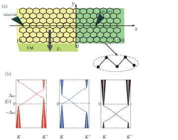
A two-terminal FS/NS device is schematically shown in figure 1, where the left-hand semi-infinite silicene nanoribbon is deposited on an ferromagnetic insulator that can induce an exchange field in the FS region, while the right-hand one is the NS on a ordinary nonmagnetic substrate. Meanwhile, an electric field is applied perpendicularly to the silicene sheet in the FS region between the top gate and the back gate which can induce sublattice potentials. The source electrode injects electrons into the FS while the drain electrode in the NS collects electrons.
We start with the tight-binding Hamiltonian of a silicene ribbon including the SOC [26]
| (2.1) |
where is the creation (annihilation) operator for an electron with spin on site , brackets and denote the summations over all the nearest and next-nearest neighbor sites. In the first term, denotes the on site energy of the FS (NS) region which can be controlled by varying the gate voltage or by doping the underlying substrate, is the exchange field in the FS region and the last one denotes the stagger on-site potential by a perpendicular electric field with the stagger potential amplitude , in which when represents a buckled up (down) atom. The second and third terms represent the nearest and next-nearest coupling with the hopping energy , and the effective SOC strength . is the pauli matrix of spin, and correspond to the anticlockwise and clockwise next-nearest-neighboring hopping with respect to the positive axis, respectively. The last term in equation (2.1) represents the Hamiltonian of the source and the detector leads described in the space and their coupling to the silicene lattices . Here, represent the source and the detecting electrodes and is the annihilation (creation) operator of the electrons in the electrode .
From equation (2.1) we get to know that a silicene will exhibit interesting topological properties and a discussion on its features is quite helpful prior to the numerical calculations. Figure 1 (b) shows the band structure in the FS and NS region with the zigzag edge. The most notable characteristic is the SOC gap which reads , between which the edge state bands connect the electron and the hole dispersions of different valleys. When the exchange field is involved, the two spin bands move up and down, so that one spin can be in the gap while the other one can lie in the conduction (valence) band by tuning the gate voltage. If the stagger potential is present, the energy gaps for the two valleys are not identical anymore and they are resolved, assuming for spin up and the reverse for spin down. As , the gap closes, but when it increases again the gap revives and enlarges and the system turns into a band insulator. For armchair ribbons, the two valleys can also become distinguishable although they overlap with each other under the perpendicular electric field.
When the flow of electrons is injected into a silicene in the FS region from a point electrode, the response signal is induced everywhere in the NS region. In order to investigate the spin injection efficiency in the silicene FS/NS junction, we will consider the response of the local particle density to the electrons injected from the source electrode. In a small bias limit and at zero temperature, the variation of the local particle density of spin per voltage is given by [27]
| (2.2) |
where the trace is over the local lattice sites coupling with the drain electrode. is the retarded (advanced) Green’s function and is given by [28]
| (2.3) |
where is the Fermi energy, is a unit matrix, is the first three terms in equation (2.1), and is the self-energy of the source (drain) electrodes. in equation (2.2) is the linewidth function of the source electrode. In actual calculations, we set the average value of the six discrete sites in a unit cell of honeycomb lattice as a real local quantity.
3 Results and discussions
In the numerical calculations, we set the nearest-neighbor carbon-carbon distance nm, the second nearestneighbor distance nm, the hopping energy eV and the SOC strength as in a real silicene sample.
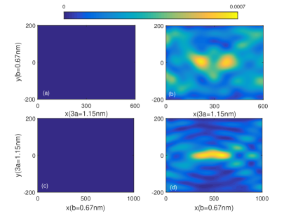
In figure 2, we present the local particle density variation of each spin in the NS region for an armchair and zigzag ribbon. It is shown that for the spin down species, the approaches zero in the whole NS region and the total quantity is of the order of . This clearly indicates that the spin down species is nearly non-existent because its Fermi energy lies in the energy gap. However, for the spin up species, the has a certain quantity in the NS region and reaches a maximum at the symmetry point of the source electrode which is caused by the negative refraction due to the Klein tunneling effect [25]. Meanwhile, the total quantity of in the whole NS region is 56.8 for the armchair ribbon and 63.2 for the zigzag ribbon. Therefore, the spin up species is distributed everywhere in the NS region and the complete spin injection is realized in the FS/NS junction. In fact, a pure spin injection can always occur as long as and so as to ensure that the Fermi energy of the two spin species locates inside and outside the bulk gap, respectively.
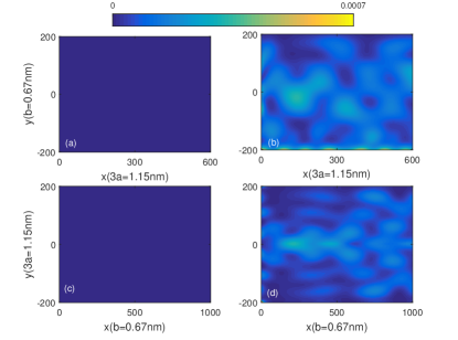
In figure 2 (b) and (d), the spin up electrons scattered in the NS region originate from two different valleys because they are still degenerate in the momentum space, meaning that one valley contributes half of the total quantity of in the NS region. As mentioned above, the presence of an electric field can adjust the bulk gap width of each valley. For instance, the bulk gap at the valley of spin up (down) enlarges but it shrinks at valley, as shown in figure 1 (b). When the Fermi energy locates in the gap of the valley of both spins by tuning the electric field, the spin up electrons in the region merely originate from the valley, the results being shown in figure 3 (b) and (d). As is shown, decreases as compared with figure 2 (b) and (d) in figure 3 (b) and (d), and the total quantity of in the whole NS region is 27.4 for the armchair ribbon and 30.8 for the zigzag ribbon which is about half the total quantity of figure 2 (b) and (d) due to the single valley contributions. Generally speaking, the single valley spin injection arises when and , or and for the case.
In the above, we only consider a spin injection in a bipolar silicene ribbon, for instance, the carriers are hole-like and electron-like on both sides of the interface. However, the results are not limited to the bipolar system provided that one spin species lies in the bulk gap while the other one is not. Moreover, the shape of the interface, a sharp or a smooth one, will not affect the spin injection which makes it feasible in a real experimental fabrication.
4 Conclusion
To conclude, we have studied a pure spin injection in the FS/NS junction and found that only one spin species can emerge in the NS region and the other one is eliminated by tuning the gate voltage in the FS region. Moreover, the spin species can originate from one valley at a certain electric field. The results are particularly interesting in view of the application for spintronics, which might be observable in doped silicene. Our findings may provide a valuable guidance for designing and fabricating spin devices based on a silicene ribbon in practical applications.
Acknowledgements
This work is supported by the National Natural Science Foundation of China (Nos. 11447218, 11547189, 11447216, 11404278), the Science Foundation of Guizhou Science and Technology Department under grant No. QKHJZ[2015]2150, and the Science Foundation of Guizhou Provincial Eduction Department under grant No. QJHKYZ[2016]092.
References
- [1] Vogt P., De Padova P., Quaresima C., Avila J., Frantzeskakis E., Asensio M.C., Resta A., Ealet B., Le Lay G., Phys. Rev. Lett., 2012, 108, No. 15, 155501, doi:10.1103/PhysRevLett.108.155501.
- [2] Ezawa M., Phys. Rev. Lett., 2013, 110, No. 2, 026603, doi:10.1103/PhysRevLett.110.026603.
- [3] Wang J., Deng S., Liu Z., Liu Z., Natl. Sci. Rev., 2015, 2, No. 1, 22, doi:10.1093/nsr/nwu080.
- [4] Cahangirov S., Topsakal M., Aktürk E., Şahin H., Ciraci S., Phys. Rev. Lett., 2009, 102, No. 23, 236804, doi:10.1103/PhysRevLett.102.236804.
- [5] Xu Y., Yan B., Zhang H.-J., Wang J., Xu G., Tang P., Duan W., Zhang S.-C., Phys. Rev. Lett., 2013, 111, No. 13, 136804, doi:10.1103/PhysRevLett.111.136804.
- [6] Hajati Y., Rashidian Z., AIP Adv., 2016, 6, No. 2, 025307, doi:10.1063/1.4942043.
- [7] Ezawa M., Phys. Rev. Lett., 2012, 109, No. 5, 055502, doi:10.1103/PhysRevLett.109.055502.
- [8] Ezawa M., New J. Phys., 2012, 14, No. 3, 033003, doi:10.1088/1367-2630/14/3/033003.
- [9] Aufray B., Kara A., Vizzini S., Oughaddou H., Léandri C., Ealet B., Le Lay G., Appl. Phys. Lett., 2010, 96, No. 18, 183102, doi:10.1063/1.3419932.
- [10] De Padova P., Quaresima C., Ottaviani C., Sheverdyaeva P.M., Moras P., Carbone C., Topwal D., Olivieri B., Kara A., Oughaddou H., Aufray B., Le Lay G., Appl. Phys. Lett., 2010, 96, No. 26, 261905, doi:10.1063/1.3459143.
- [11] Tao L., Cinquanta E., Chiappe D., Grazianetti C., Fanciulli M., Dubey M., Molle A., Akinwande D., Nat. Nanotechnol., 2015, 10, No. 3, 227, doi:10.1038/nnano.2014.325.
- [12] Bishnoi B., Ghosh B., RSC Adv., 2013, 3, No. 48, 26153, doi:10.1039/c3ra43491e.
-
[13]
Yamakage A., Ezawa M., Tanaka Y., Nagaosa N., Phys. Rev. B, 2013, 88, No. 8, 085322,
doi:10.1103/PhysRevB.88.085322. - [14] Liu C.-C., Feng W., Yao Y., Phys. Rev. Lett., 2011, 107, No. 7, 076802, doi:10.1103/PhysRevLett.107.076802.
- [15] Pan H., Li Z., Liu C.-C., Zhu G., Qiao Z., Yao Y., Phys. Rev. Lett., 2014, 112, No. 10, 106802, doi:10.1103/PhysRevLett.112.106802.
- [16] Ezawa M., Phys. Rev. B, 2013, 87, No. 15, 155415, doi:10.1103/PhysRevB.87.155415.
- [17] Tsai W.-F., Huang C.-Y., Chang T.-R., Lin H., Jeng H.-T., Bansil A., Nat. Commun., 2013, 4, 1500, doi:10.1038/ncomms2525.
- [18] Gupta G., Lin H., Bansil A., Jalil M.B.A., Huang C.-Y., Tsai W.-F., Liang G., Appl. Phys. Lett., 2014, 104, No. 3, 032410, doi:10.1063/1.4863088.
- [19] Yokoyama T., Phys. Rev. B, 2013, 87, No. 24, 241409, doi:10.1103/PhysRevB.87.241409.
- [20] Han W., Wang W.H., Pi K., McCreary K.M., Bao W., Li Y., Miao F., Lau C.N., Kawakami R.K., Phys. Rev. Lett., 2009, 102, No. 13, 137205, doi:10.1103/PhysRevLett.102.137205.
- [21] Ando Y., Hamaya K., Kasahara K., Kishi Y., Ueda K., Sawano K., Sadoh T., Miyao M., Appl. Phys. Lett., 2009, 94, No. 18, 182105, doi:10.1063/1.3130211.
- [22] Li C.H., van ’t Erve O.M.J., Jonker B.T., Nat. Commun., 2011, 2, 245, doi:10.1038/ncomms1256.
- [23] Tang J., Wang K.L., Nanoscale, 2015, 7, No. 10, 4325, doi:10.1039/C4NR07611G.
- [24] Zhang S., Dayeh S.A., Li Y., Crooker S.A., Smith D.L., Picraux S.T., Nano Lett., 2013, 13, No. 2, 430, doi:10.1021/nl303667v.
- [25] Tian H.Y., Chan K.S., Wang J., Phys. Rev. B, 2012, 86, No. 24, 245413, doi:10.1103/PhysRevB.86.245413.
-
[26]
Yang M., Song X.L., Chen D.H., Bai Y.K., Phys. Lett. A, 2015, 379, No. 16–17, 1149,
doi:10.1016/j.physleta.2015.02.021. -
[27]
Tao W.W., Liu B., Dai Q., Wang S.-K., Commun. Theor. Phys., 2014, 61, No. 3, 391,
doi:10.1088/0253-6102/61/3/20. - [28] Xing Y., Wang J., Sun Q.-F., Phys. Rev. B, 2010, 81, No. 16, 165425, doi:10.1103/PhysRevB.81.165425.
Ukrainian \adddialect\l@ukrainian0 \l@ukrainian Досконала спiнова iнжекцiя на переходi FS/NS силiцен Г.-Я. Тьян, Т. Хю, Г. Люо, Ч.-Д. Рен
Фiзичний факультет, Технологiчний iнститут Янченг, Цзянсу 224051, Китай
Фiзичний факультет, Нормальний коледж Зунию, Гуйжоу 563002, Китай