Topology Optimized Multi-layered Meta-optics
Abstract
We propose a general topology optimization framework for metasurface inverse design that can automatically discover highly complex multi-layered meta-structures with increased functionalities. In particular, we present topology-optimized multi-layered geometries exhibiting angular phase control, including a single-piece nanophotonic metalens with angular aberration correction as well as an angle-convergent metalens that focuses light onto the same focal spot regardless of the angle of incidence.
pacs:
78.67Pt, 42.15Eq, 42.15Fr, 42.30Va, 42.79BhPhase-gradient metasurfaces yu2011light have recently received widespread attention due to their successful applications in important technologies such as beam steering, imaging and holography aieta2015multiwavelength ; arbabi2015dielectric ; khorasaninejad2016metalenses . Although they offer many advantages in terms of size and scaling over traditional refractive bulk optics, their capabilities are limited with respect to spectral and angular control estakhri2016wave ; arbabi2017fundamental . Theoretical analysis of ultra-thin metasurfaces suggests that to circumvent such limitations, it might be necessary to employ exotic elements such as active permittivities (e.g. optical gain), bi-anisoptropy, magnetic materials, or even nonlocal response estakhri2016wave . Although materials with such properties might be found in the radio-frequency (RF) regime, they are not readily available at optical frequencies. Alternatively, device functionalities may be enhanced by increasingly complex geometric design. For instance, multi-functional devices have been demonstrated by cascading a few layers of metasurfaces, each of which comprises typical dielectric materials arbabi2014planar ; arbabi2016miniature . So far, most of these multi-layered meta-structures (MMS) fall into a category of structures where each layer is sufficiently far apart from the other and can be considered independently.
In this letter, we introduce a different class of MMS involving several, tightly spaced layers which allow richer physical interactions within and between layers and thereby offer increased functionalities. The key property of these MMS is that each layer cannot be treated independently of the other but must be considered integrally in the design process. Such a consideration often leads to a greatly extended design space that cannot be handled by traditional design methods, which rely on pre-compiled libraries of intuitive geometrical elements. Below, we propose a general topology optimization (TO) framework that can automatically discover highly complex MMS with broad functionalities. As a proof of concept, we present two TO multi-layered geometries exhibiting angular phase control: a single-piece nanophotonic metalens with angular aberration correction (Fig. 1a) and an angle-convergent metalens that focuses light onto the same focal spot regardless of incident angle (Fig. 1b).
Inverse design formulation.— Topology optimization (TO) is an efficient computational technique that can handle an extensive design space, considering the dielectric permittivity at every spatial point as a degree of freedom (DOF) Yablonovitch05 ; Jensen11 . A typical TO electromagnetic problem can be written as:
| (1) | ||||
| (2) | ||||
| (3) |
Here, the DOFs are related to the position-dependent dielectric profile via , where denotes the relative permittivity of the structural (background) dielectric material. While may take intermediate values between 0 and 1, one can ensure a binary (digital) structure via penalization and filter projection methods Jensen11 . The objective and constraint are often functions of the electric field , a solution of Maxwell’s equation,
| (4) |
which yields the steady-state in response to incident currents at a given frequency . While the solution of (4) is straightforward and commonplace, the key to making optimization problems tractable is to obtain a fast-converging and computationally efficient adjoint formulation of the problem. Within the scope of TO, this requires efficient calculations of the derivatives at every spatial point , performed by exploiting the adjoint-variable method Jensen11 .
Recently, inverse-design techniques based on TO have been successfully applied to a variety of photonic systems including on-chip mode splitters, nonlinear frequency converters and Dirac cone photonic crystals Jensen11 ; liang2013formulation ; lu2013nanophotonic ; men2014robust ; piggott2015inverse ; shen2015integrated ; lin2016cavity ; ZinEP3 ; ZinZIM . However, to the best of our knowledge, there is an apparent lack of large-scale computational techniques specifically tailored for metasurface design, with the possible exception of Ref. JFan17 , which is limited to grating deflectors. Here, we introduce a general optimization framework for designing a generic meta-optics device, single or multi-layered, with arbitrary phase response. The key to our formulation is the familiar superposition principle: given a desired phase profile , the ideal wavefront and the complex electric field will constructively interfere if and only if their phase difference vanishes. Defining for a given polarization , we define the following optimization function:
| (5) |
where and the spatial integration is performed over a reference plane (typically one or two wavelengths away from the meta-device) where is defined. Note that is none other than a spatially-averaged cosine of the phase difference between and ,
with the property . Therefore, can be used to gague and characterize the performance of the device under construction, with indicating that the algorithm has converged to an optimal solution. In practice, the optimization algorithms discovered devices with for many of the problems under investigation.
Angular phase control.— An attractive feature of nano-scale meta-devices is their potential for arbitrary wavefront manipulation under various control variables including wavelength, polarization or incident angle. Although spectral and polarization control have been explored in a number of previous works aieta2015multiwavelength ; mueller2017metasurface , to the best of our knowledge, angular control has not been achieved so far. In fact, realizing angular control in traditional single-layer ultra-thin metasurfaces might prove fundamentally impossible since the interface is constrained by the generalized Snell’s laws yu2011light . On the other hand, MMS with thicknesses on the order of a wavelength or more (whose internal operation cannot be described via ray optics) can overcome such a limitation; in principle, they can be engineered to exhibit directionality even though conventional approaches which rely on intuitive, hand designs might prove unequal to such a task. Here, we leverage our optimization algorithm to develop multi-functional structures where an arbitrary phase response that varies with the angle of incidence can be imprinted on the same device.
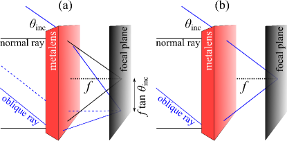
The traditional objective in the design of metalenses is the creation of a single, hyperbolic phase profile, , characterized by the focal length , in response to a normally incident plane wave aieta2015multiwavelength . Here, denotes the center of the lens whereas denotes an arbitrary phase reference that can be varied as an additional degree of freedom in the metasurface design khorasaninejad2017achromatic . As discussed in the Ref. aieta2013aberrations , such a design is free of spherical aberrations but still suffer from angular and off-axis aberrations such as coma and field curvature. These errors arise out of an incorrect phase profile that skews the oblique off-axis rays. A corrected phase profile free from aberration is therefore necessarily angle-dependent, as given by:
|
|
Note that the above expression can be deduced by considering the optical path length contrast between a generic ray and the orthonormal ray directed towards a focusing spot laterally shifted by (see Fig. 1a, blue dashed line). Here, we leverage our TO algorithm to design a 2D miniature angle-corrected metalens that exactly embodies the ideal angle-dependent phase profile given above. Note that though our miniature design is a proof-of-concept theoretical prototype, it is completely straightforward (though computationally intensive) to design a full 3D wide-area (centimeter-scale) single-piece monochromatic aberration-free lens using our TO technique. We emphasize that such a “next generation” lens fundamentally differs from the traditional aberration-corrected doublet because the latter exclusively relies on classical ray tracing techniques whereas the former intricately exploits nano-scale electromagnetic effects to achieve angular control.
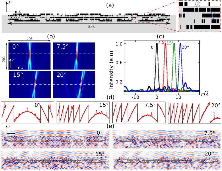
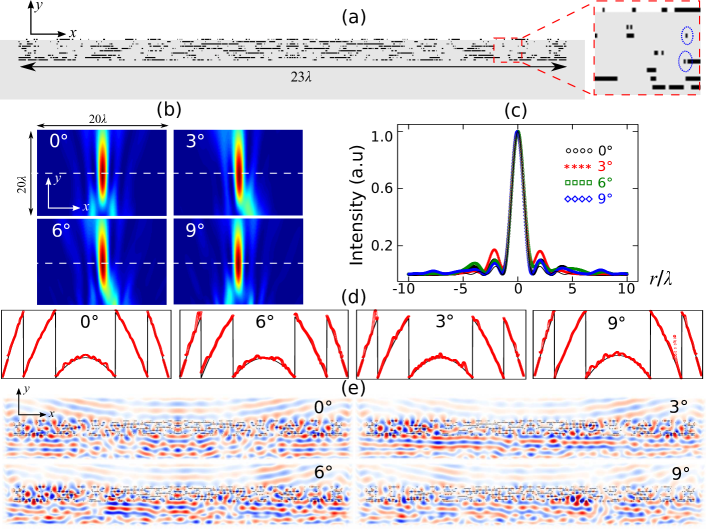
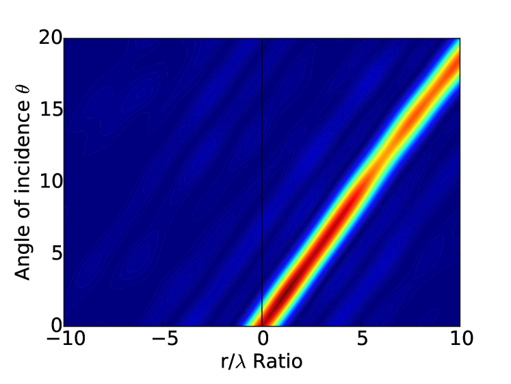
We design a lens with an NA of 0.35 and a focal length of . The device consists of five layers of topology-optimized aperiodic silicon gratings (invariant along ) against amorphous alumina background (Fig. 2a). Each silicon layer is thick and is separated by alumina gaps. We specifically chose silicon and alumina with a view to eventual fabrication at mid or far IR wavelengths () by stacking patterned 2D slabs via repeated lithography, material deposition and planarization processes 3d2 ; 3d4 . The entire lens has a thickness of , offering ample space for complex electromagnetic interactions while, at the same time, maintaining orders of magnitude smaller thickness compared to traditional multi-lens systems. The lens is aberration corrected for four incident angles as well as their negative counterparts . Note that the largest possible angle for diffraction-limited focusing is and is determined by the numerical aperture. For simplicity, we consider off-axis propagation in the plane with an -polarized electric field parallel to the direction of the gratings, . FDTD analysis of the far field (Fig. 2b) reveals focusing action with diffraction limited intensity profiles (Fig. 2c), while the transmission efficiencies average around for the four angles. To evaluate the deviation of our design from the ideal phase profile, we computed the wave aberration function (WAF) for each angle aieta2013aberrations , obtaining , which clearly satisfy the Marèchal criterion except for the incident angle. The errors in the latter case primarily arise from the difficulty over optimizing the extremities of the lens, which can be mitigated by extending the optimized lens area (or equivalently designing a larger NA). It is worth noting that the residual phase errors apparent in the optimized design primarily stem from a need to force the optimal design to be binary while being constrained by a limited resolution. In this work, we implemented a spatial resolution step size over a -long simulation domain while our optimization algorithm handles approximately 5600 degrees of freedom. These parameters are solely dictated by the limited computational resources currently available to us. We find that without the binary constraint (i.e. when each DOF is allowed to take intermediate values between 0 and 1), the optimal designs easily achieve perfect phase profiles with WAFs smaller than . We expect that given better computational facilities, optimization over higher resolution domains will lead to fully binary structures that also preserve vanishing .
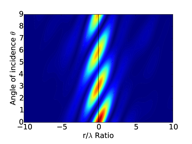
Next, to demonstrate the versatility of our approach, we design a 2D metalens that focuses light onto the same spot regardless of the angle of incidence (Fig. 1b) – a device which we will choose to call angle-convergent metalens. Specifically, we impose the phase profile on the outgoing field under multiple discrete incident angles . The lens has an NA of 0.35 and a focal length of . The lens materials consist of ten layers of thick silicon in silica separated by gaps (Fig. 3a), making the entire device approximately one thick. Such a device can be fabricated using advanced 3D photonic integration techniques 3d2 , including those enabled by CMOS foundries 3d1 . Far field analysis (Fig. 3b) shows focusing action at the same focal spot for all the angles. Although the field intensities at the focal spot do not exactly follow the profile of an ideal Airy disk due to residual phase errors, their bandwidth (aka full width at half maximum) clearly satisfies the diffraction limit (Fig. 3c). The diffraction-limited focusing is also consistent with small WAFs which are found to satisfy the Marèchal criterion: . The transmission efficiency of the device averages around 15% over all angles.
Conclusion and outlook.— To summarize, we proposed a general optimization framework for inverse design of multi-layered meta-optics. We leveraged our formulation to engineer angular phase control in multi-layered metalens. It is important to note that, in this paper, as we focus on establishing the validity and versatility of our optimization approach, we have not sought to pursue “the best possible design” for any particular problem that we chose to investigate. For example, the number, positioning and thicknesses of layers are arbitrarily chosen in each problem. It is entirely possible that depending on the desired level of performance, one can achieve viable designs using fewer and/or thicker layers, which could render the entire device even thinner and easier to fabricate.
While the optimization framework we have proposed exclusively focuses on phase, work is currently under way to implement additional features such as amplitude uniformity and high efficiency constraints, which can be straightforwardly added to our formulation. Although the addition of extra conditions would presumably strain the optimization process, we expect that a full 3D multi-layered device platform should be able to accommodate any additional demands. Ultimately, we surmise that multi-layered volumetric structures (no more than a few wavelengths thick) will help deliver unprecedented wavefront manipulation capabilities at the nano-scale that involve phase, intensity and polarization control as well as spectral and angular dispersion engineering altogether in a single device. The TO technique is by far the most efficient tool that can handle the enormous design space available to such platforms. Although fabrication of multi-layered nanostructures might prove challenging for shorter operational wavelengths, they can be readily implemented in mid to far IR regimes, through state-of-the-art 3D fabrication technologies 3d2 such as two-photon lithography 3d5 and laser writing processes 3d3 , advanced foundry access 3d1 as well as ultra-high resolution EUV lithography euv .
Acknowledgements.— We would like to thank Raphael Pestourie, Steven Johnson, Pawel Latawiec, Robert Devlin, Wei-Ting Chen and Alexander Zhu for useful discussions. Z. Lin is supported by the National Science Foundation Graduate Research Fellowship Program under Grant No. DGE1144152. The work was partially supported by the Air Force Office of Scientific Research (MURI grant no. FA9550-14-1-0389), by the National Science Foundation under Grant No. DMR-1454836, by the National Science Foundation under EFRI-1005093 and by the Princeton Center for Complex Materials, a MRSEC supported by NSF Grant No. DMR 1420541.
References
- [1] Nanfang Yu, Patrice Genevet, Mikhail A Kats, Francesco Aieta, Jean-Philippe Tetienne, Federico Capasso, and Zeno Gaburro. Light propagation with phase discontinuities: generalized laws of reflection and refraction. science, 334:333, 2011.
- [2] Francesco Aieta, Mikhail A Kats, Patrice Genevet, and Federico Capasso. Multiwavelength achromatic metasurfaces by dispersive phase compensation. Science, 347:1342, 2015.
- [3] Amir Arbabi, Yu Horie, Mahmood Bagheri, and Andrei Faraon. Dielectric metasurfaces for complete control of phase and polarization with subwavelength spatial resolution and high transmission. Nature Nanotechnology, 10:937, 2015.
- [4] Mohammadreza Khorasaninejad, Wei Ting Chen, Robert C Devlin, Jaewon Oh, Alexander Y Zhu, and Federico Capasso. Metalenses at visible wavelengths: Diffraction-limited focusing and subwavelength resolution imaging. Science, 352:1190, 2016.
- [5] Nasim Mohammadi Estakhri and Andrea Alù. Wave-front transformation with gradient metasurfaces. Physical Review X, 6:041008, 2016.
- [6] Amir Arbabi and Andrei Faraon. Fundamental limits of ultrathin metasurfaces. Scientific Reports, 7:43722, 2017.
- [7] Amir Arbabi, Yu Horie, and Andrei Faraon. Planar retroreflector. In Lasers and Electro-Optics (CLEO), page 1, 2014.
- [8] Amir Arbabi, Ehsan Arbabi, Seyedeh Mahsa Kamali, Yu Horie, Seunghoon Han, and Andrei Faraon. Miniature optical planar camera based on a wide-angle metasurface doublet corrected for monochromatic aberrations. Nature Communications, 7, 2016.
- [9] Chiu Y Kao, Stanley Osher, and Eli Yablonovitch. Maximizing band gaps in two-dimensional photonic crystals by using level set methods. Applied Physics B: Lasers and Optics, 81:235, 2005.
- [10] Jakob S Jensen and Ole Sigmund. Topology optimization for nano-photonics. Laser and Photonics Reviews, 5:308, 2011.
- [11] Xiangdong Liang and Steven G Johnson. Formulation for scalable optimization of microcavities via the frequency-averaged local density of states. Optics express, 21:30812, 2013.
- [12] Jesse Lu and Jelena Vučković. Nanophotonic computational design. Optics express, 21:13351, 2013.
- [13] Han Men, Karen YK Lee, Robert M Freund, Jaime Peraire, and Steven G Johnson. Robust topology optimization of three-dimensional photonic-crystal band-gap structures. Optics express, 22:22632, 2014.
- [14] Alexander Y Piggott, Jesse Lu, Konstantinos G Lagoudakis, Jan Petykiewicz, Thomas M Babinec, and Jelena Vučković. Inverse design and demonstration of a compact and broadband on-chip wavelength demultiplexer. Nature Photonics, 9:374, 2015.
- [15] Bing Shen, Peng Wang, Randy Polson, and Rajesh Menon. An integrated-nanophotonics polarization beamsplitter with 2.4 2.4 m2 footprint. Nature Photonics, 9:378, 2015.
- [16] Zin Lin, Xiangdong Liang, Marko Lončar, Steven G Johnson, and Alejandro W Rodriguez. Cavity-enhanced second-harmonic generation via nonlinear-overlap optimization. Optica, 3:233, 2016.
- [17] Zin Lin, Adi Pick, Marko Lončar, and Alejandro W Rodriguez. Enhanced spontaneous emission at third-order dirac exceptional points in inverse-designed photonic crystals. Physical Review Letters, 117:107402, 2016.
- [18] Zin Lin, Lysander Christakis, Yang Li, Eric Mazur, Alejandro W Rodriguez, and Marko Lončar. Topology-optimized Dual-Polarization Dirac Cones. ArXiv e-prints, 2017.
- [19] David Sell, Jianji Yang, Sage Doshay, Rui Yang, and Jonathan A Fan. Large angle, multi-functional metagratings based on freeform multi-mode geometries. Nano Letters, 2017.
- [20] Jan P. Balthasar Mueller, Noah A Rubin, Robert C Devlin, Benedikt Groever, and Federico Capasso. Metasurface polarization optics: Independent phase control of arbitrary orthogonal states of polarization. Physical Review Letters, 118:113901, 2017.
- [21] Mohammadreza Khorasaninejad, Zhujun Shi, Alexander Y Zhu, Wei-Ting Chen, Vyshakh Sanjeev, Aun Zaidi, and Federico Capasso. Achromatic metalens over 60 nm bandwidth in the visible and metalens with reverse chromatic dispersion. Nano Letters, 17:1819, 2017.
- [22] Francesco Aieta, Patrice Genevet, Mikhail Kats, and Federico Capasso. Aberrations of flat lenses and aplanatic metasurfaces. Optics express, 21:31530, 2013.
- [23] Nicolás Sherwood-Droz and Michal Lipson. Scalable 3d dense integration of photonics on bulk silicon. Optics express, 19:17758, 2011.
- [24] Minghao Qi, Elefterios Lidorikis, Peter T Rakich, Steven G Johnson, JD Joannopoulos, Erich P Ippen, and Henry I Smith. A three-dimensional optical photonic crystal with designed point defects. Nature, 429:538, 2004.
- [25] Michael Hochberg and Tom Baehr-Jones. Towards fabless silicon photonics. Nature Photonics, 4:492, 2010.
- [26] Timo Gissibl, Simon Thiele, Alois Herkommer, and Harald Giessen. Two-photon direct laser writing of ultracompact multi-lens objectives. Nature Photonics, 10:554, 2016.
- [27] Fabian Niesler and Yann Tanguy. 3d printers for the fabrication of micro-optical elements. Optik & Photonik, 11:44, 2016.
- [28] Charles W Gwyn, R Stulen, D Sweeney, and D Attwood. Extreme ultraviolet lithography. Journal of Vacuum Science & Technology B: Microelectronics and Nanometer Structures Processing, Measurement, and Phenomena, 16:3142, 1998.
I Supplement
II Phase profile of an ideal aberration-free lens
Here, we examine the angle-dependent phase profile necessary to correct monochromatic aberrations in a lens:
| (S1) |
Here, is the origin of the lens. It is easily seen that the aberration-corrected is simply a hyperbolic profile shifted by a distance which is the location of focal spot in the far field. When the angle of incidence is zero, we obtain the familiar hyperbolic phase profile for the normal incidence. Given , we can exactly compute the far field by convoluting with the standard Green’s function propagator:
| (S2) |
In our paper, we have exactly computed the ideal far field intensity profile based on the convolution integral above (Eq. S2) and compared it with the simulated far field of the optimized design for each incident angle. It should be noted that for , the width (FWHM) of the far field begins to violate the diffraction limit .
III Comparison against standard normal-incidence metalens design
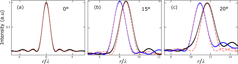
We examine the standard single-layered metalens () with the same parameters as our topology-optimized aberration-corrected design given in the main text. Precisely speaking, a standard lens is one which is optimized only for diffraction-limited focusing at the normal incidence . Figure S1a (black circle data points) shows that the standard lens ensures perfect diffraction limited focusing along the ideal Airy profile (red dashed line). For incident angle (Fig. S1b), the field maximum (black circle data points) of the standard lens deviates from the ideal spot on the focal plane while exhibiting slight broadening and marked asymmetry. Note that a displaced replica of the ideal profile (red dashed line) is superimposed on the black circle data points for an easy comparison of the two linewidths between the standard and ideal lenses. Blue circle data points represent the field profile of the topology-optimized angle-corrected meta-lens which almost perfectly follows the ideal profile. Deviations in the standard lens are even more pronounced for the larger incident angle of (Fig. S1c).
IV Angle Sweep
In Figure S2, we examine the topology-optimized designs for different angles of incidence. The aberration-corrected meta-lens (Figure 2(a)) has a continuous focusing function while the angle-convergent on-axis focusing meta-lens has discrete focal spots at the optimized angles of incidence (Figure 2(b)). We expect the result can be further improved by optimizing many more angles.
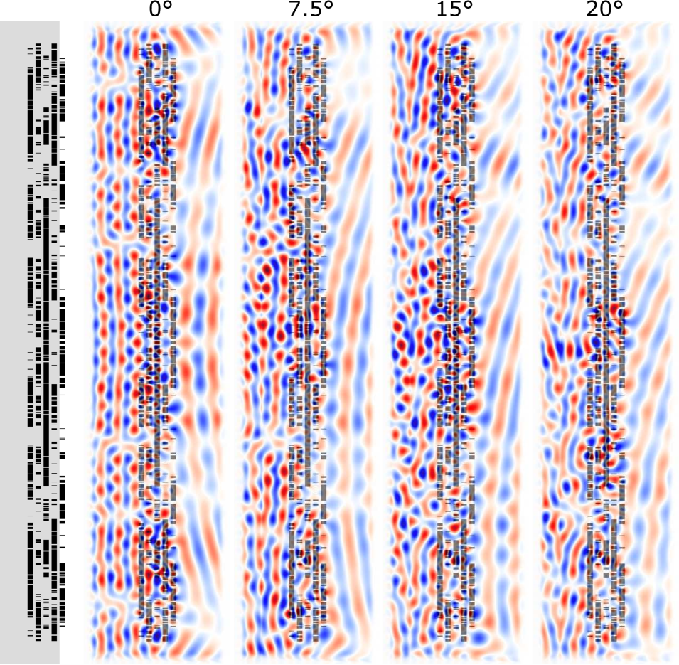
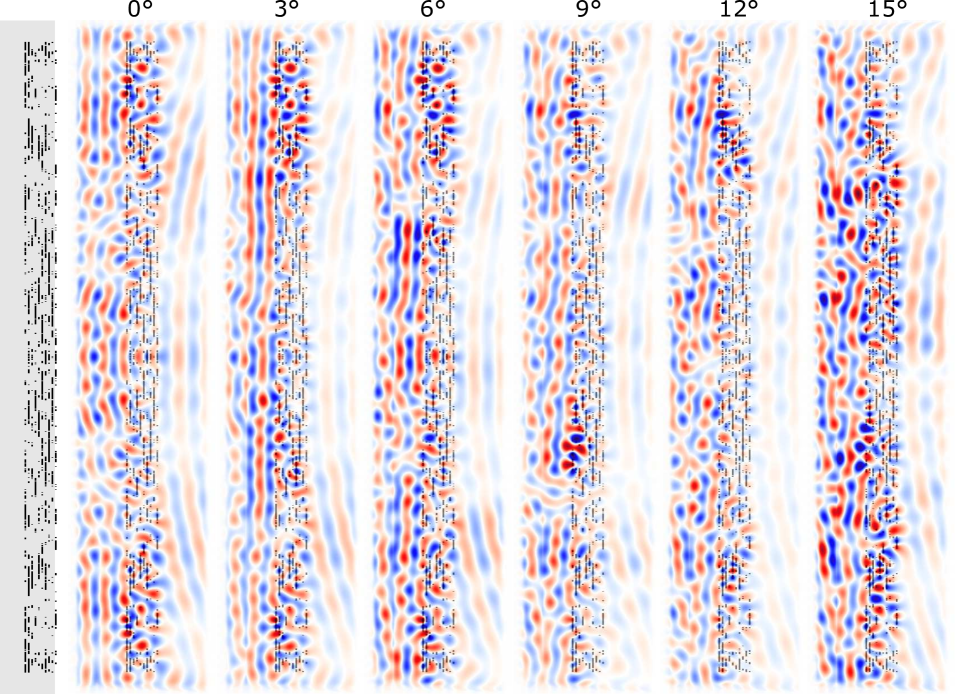
V Detailed structures of the topology-optimized meta-lenses and field profiles
Detailed structural images of the angle-corrected and angle-convergent metalenses are given in Figs. S3 and S4, together with the corresponding “out-of-page” -polarization near-field profiles showing almost perfect spherical wavefronts. Note that the design of the angle-convergent metalens (Fig. S4) has been tweaked to accommodate on-axis focusing at the larger angles of and . Although we achieve diffraction-limited focusing for these angles as well (not shown), the transmission efficiencies become much smaller . In future works, this issue will be fixed by explicitly incorporating a high-transmission efficiency constraint into the optimization process.