An argon ion beam milling process for native layers enabling coherent superconducting contacts
Abstract
We present an argon ion beam milling process to remove the native oxide layer forming on aluminum thin films due to their exposure to atmosphere in between lithographic steps. Our cleaning process is readily integrable with conventional fabrication of Josephson junction quantum circuits. From measurements of the internal quality factors of superconducting microwave resonators with and without contacts, we place an upper bound on the residual resistance of an ion beam milled contact of at a frequency of . Resonators for which only 6% of the total foot-print was exposed to the ion beam milling, in areas of low electric and high magnetic field, showed quality factors above in the single photon regime, and no degradation compared to single layer samples. We believe these results will enable the development of increasingly complex superconducting circuits for quantum information processing.
The research field of superconducting quantum electronics has been developing at an accelerated pace for the last two decades, and it is now one of the leading candidates for the implementation of quantum mechanical computational machines which could eventually outperform classical computers Devoret and Schoelkopf (2013). On the path to achieving this scientific landmark, microelectronic quantum circuits are required to become increasingly complex, to implement an ever growing set of functionalities, such as: fast single and multiple qubit operations Plantenberg et al. (2007); Barends et al. (2014), quantum non-demolition readout Wallraff et al. (2004); Castellanos-Beltran and Lehnert (2007); Vijay et al. (2011); Abdo et al. (2011), remote qubit entanglement Ristè et al. (2013); Steffen et al. (2013); Chow et al. (2014); Roch et al. (2014) and qubit-qubit interactions Berkley (2003); Steffen et al. (2006); Majer et al. (2007), or autonomous feedback Shankar et al. (2013); Geerlings et al. (2013). Not only are these goals challenging by themselves, but it is paramount that they are achieved without compromising on the quantum coherence of the device.
Several quantum circuit integration approaches are currently pursued with promising results. Flip-chip strategies Minev et al. (2016); Brecht et al. (2015) or complex 2.5D circuit designs Kelly et al. (2015); Ristè et al. (2015) have recently shown coherence comparable with state of the art single devices Paik et al. (2011); Rigetti et al. (2012); Barends et al. (2013). Their fabrication often requires several lithography steps, involving different clean-room technologies. One of the challenges of integrating different microelectronic fabrication layers Sandberg et al. (2012); Vissers et al. (2012); Braumüller et al. (2015), is to obtain not only a very good galvanic contact, but also a very high quality factor at microwave frequencies.
Aluminum is one of the most widely used materials for superconducting quantum electronics, thanks to the controllable and convenient growth of the oxide barrier between the electrodes of Josephson junctions, and its relatively low surface dielectric loss tangent O’Connell et al. (2008); Wang et al. (2015). However, aluminum also forms an insulating oxide when exposed to atmosphere, which has to be removed prior to contacting different lithographic layers.
In this letter we present an argon ion beam milling process to remove the native aluminum oxide, which enables the fabrication of state of the art coherent devices. We show that overlap contacts obtained using ion beam milling did not cause any measurable degradation in quality factor compared to a continuous metallic film, when embedded into microwave resonators with internal quality factors on the order of in the single photon regime.
We perform the argon ion beam milling using the Kaufman ion source connected to the load lock of a MEB 550 S shadow evaporation machine at a base pressure in the range of mbar immediately before the deposition of aluminum thin films. The parameters of the ion source during cleaning are set as follows: 4 sccm argon-gas at a beam voltage of , an accelerating voltage of and an ion current of . Between the end of the milling process and the opening of the shutter for the aluminum deposition the time interval is approximately . The rate of the aluminum deposition is . All samples are fabricated using an optical lithography lift-off technique on double-side polished thick c-plane sapphire wafers.
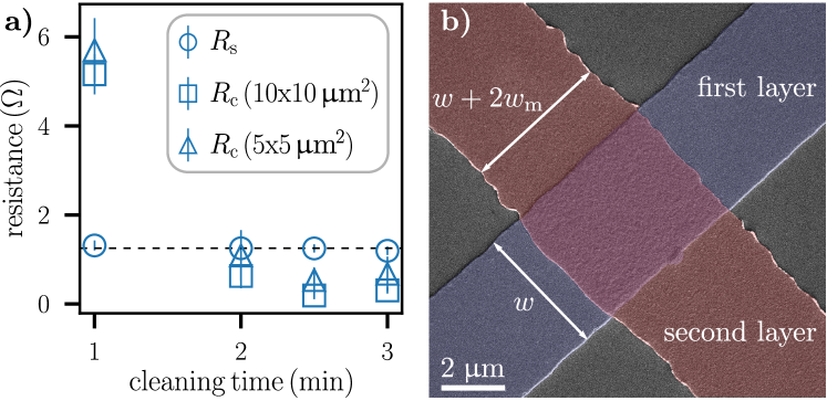
We calibrate the duration of the milling process by measuring the decrease in DC resistance of overlap contacts, as shown in Fig. 1a. After of milling the DC contact resistance is smaller than the sheet resistance of a single-layer aluminum film, which defines the measurable upper bound for in our setup. Figure 1b shows a SEM image where we can observe the effect of the aggressive cleaning step on the patterned resist: a widening of the strips by together with a roughening of the edges. By completely milling aluminum films with and without exposure to atmosphere, we estimate a ratio of 1:10 for the milling rates of native aluminum oxide and pure aluminum. Given the thicknesses of the native oxide layer () and the underlying pure aluminum thin film (), we expect comparable milling times for their removal. Therefore, it is crucial not to overetch the overlapping area of the contacts. Figure 1b shows that after of cleaning, one minute longer than what is needed for a negligible DC resistance, the first aluminum electrode is still continuous, illustrating the robustness of the process with respect to possible ion beam milling inhomogeneities.
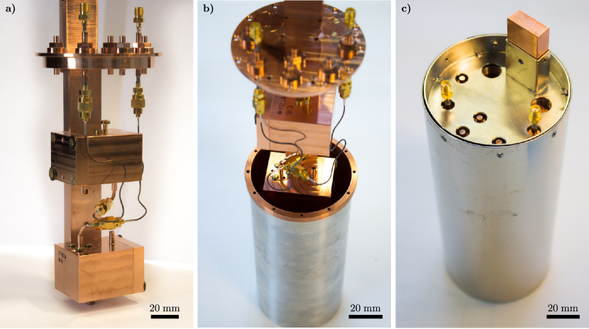
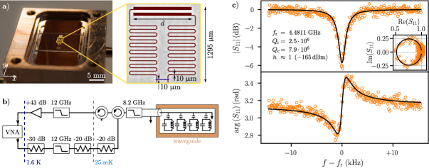
To measure the coherence of the contacts between lithographic layers we fabricate superconducting resonators with and without overlap contacts and compare their quality factors. All lithographic layers are done in conventional lift-off technique. Figure 2a shows a picture of a sapphire chip with four resonators mounted in a 3D copper waveguide sample holder, following a design that was recently used to perform simultaneous readout of fluxonium qubits Kou et al. (2017). The sample holder has a pass band of approximately starting from the cutoff frequency of the waveguide at . Inside the band, the reflection from the waveguide to the coaxial cables of our measurement setup is below . A copper cap closes and shorts the waveguide at a distance of (approximately for frequencies in the bandwidth) from the sapphire chip. Silver paste fixes the sapphire chip to the waveguide body and an indium wire seal ensures good electrical contact as well as tight sealing between the waveguide body and the cap. Two shields machined from a copper/aluminum sandwich and -metal around the closed waveguide sample holder provide IR radiation Barends et al. (2011) and magnetic shielding (see supplementary material). The entire assembly is thermally anchored to the base plate of a commercial dilution refrigerator at .
In the inset of Fig. 2a we show an optical microscope image of one of the measured resonators. For all resonators, the length of the meandering inductor is and its width is , while the capacitor length takes the values 1000, 950, 900, and , which distribute the resonant frequencies in a range of around . We deliberately design these frequencies below the cutoff frequency of the waveguide to decouple the resonators from the microwave environment and achieve coupling quality factors in the range of (see Fig. 3a). To test the quality factor of the argon ion milled overlap contacts, for half of the measured resonators the aluminum film of the meander is interrupted in the middle, and reconnected in a second lithographic step using a strip of the same width that we call bridge.
Figure 2b shows a schematic of our cryogenic measurement setup. A vector network analyzer (VNA) measures the complex response of the resonators. The input signal is in total attenuated by -100 dB, -30 dB at room temperature and -70 dB distributed at different temperature stages of the cryostat, including the attenuation of the resistive coaxial microwave cables. Two cryogenic circulators provide signal routing and isolation on the output line, respectively. A commercial high electron mobility transistor amplifier on the stage of the cryostat amplifies the outgoing signal by +43 dB. At room temperature a second commercial amplifier adds +60 dB to the signal.
Figure 2c shows a typical measured and fitted resonator response at an input power of -165 dBm corresponding to an average number of photons circulating in the resonator of . We use a circle fit routine in the complex plane to extract the quality factor and the resonant frequency Probst et al. (2015).
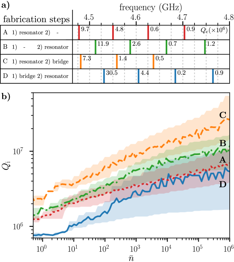
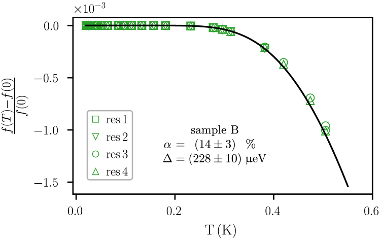
For each sample, Fig. 3 gives an overview of the fabrication sequence, the measured internal quality factors , the resonant frequencies, and corresponding coupling quality factors . Notice that the frequencies of the resonators on samples A and C are significantly lower than those of samples B and D. This can be explained by the fact that the entire resonator, except the bridge region, is deposited in lithography step 1 for samples A and C, and in step 2 for B and D. The frequency shift between the two groups of samples is caused by the ion milling step which increases the meander width (see Fig. 1) by , effectively reducing the number of squares, , for samples B and D, and thereby decreasing the kinetic inductance. The observed shift of approximately could be explained by a widening of the strip on the order of , which is consistent with the values indicated in Fig. 1b. Additionally, the milling lowers the geometric inductance of the meander, and also increases the capacitance by reducing the distance between the capacitor pads. However, these two modifications to the resonator geometry will only be on the order of 1%, the resulting changes in resonant frequency will have opposite signs, and they can therefore be neglected. We estimate that the difference between the film thickness of samples A, C () and B, D () will result in a 10 % change of the kinetic inductance fraction Gao (2008). For sample B we measured (see Fig. 4), which implies that the frequency shift between samples A, C and B, D, due to the change in kinetic inductance fraction should be less than .
The measured frequency difference between resonators fabricated in the same lithographic step without, A and B, and with a contact bridge, C and D, respectively, is only on the order of a few . Surprisingly, the resonant frequencies of samples with a contact bridge are all higher than the frequencies of the corresponding single layer resonators, indicating a negligible contribution from the kinetic inductance of the overlap contacts. The shift to higher frequencies for resonators on sample C compared to sample A could again be explained by a widening of the bridge during the argon ion milling, consistent with the arguments presented in the previous paragraph. Finally, for sample D, we expect smaller frequencies compared to sample B, however, they are measured to be significantly higher. This shift, observed for samples where the entire area of the resonator was subjected to the ion milling, could also arise from random fluctuations of the width of structures fabricated in different positions on the wafer. Possible causes for this variations include a non-uniform ion beam profile or inhomogeneities in the UV-beam exposure over the two inch diameter of the wafer.
The solid lines in Fig. 3b show the mean of all resonators for each sample as a function of the average number of circulating photons . The spread between the highest and lowest of each sample is indicated by the shaded area. We would like to emphasize that the single-layer samples A and B, and sample C, where the cleaning process is only applied to the connecting bridge, show internal quality factors larger than in the single photon regime. Remarkably, we measure the highest average on the resonators of sample C which include an ion beam milled contact bridge. From the mean internal quality factors of samples with a bridge (C, D) we extract an upper bound on the residual resistance of the contacts of (see supplementary material). From 3D finite element simulations we extract a participation ratio of the metal-substrate and metal-air interfaces of the resonator of , which is smaller than in coplanar geometries, due to the larger mode volume of the waveguide sample holder. This allows us to extract a surface dielectric loss tangent , which is in the range of commonly reported values Wang et al. (2015).
A potential inhomogeneity of the argon ion beam could have caused stronger milling of sample D and a degradation of the substrate Dunsworth et al. (2017), thereby explaining the lower quality factors of all resonators of sample D, compared to those of sample B.
To measure the kinetic inductance fraction of sample B, for which the entire surface of the resonators was subjected to the milling, we measure the temperature dependence of the resonant frequencies. The measured change of the resonant frequency as a function of temperature (see Fig. 4) is modeled using the following equation,
| (1) |
where the kinetic inductance fraction and the superconducting gap are used as fit parameters.
The fit is performed for all four resonators of sample B individually. Taking the average of all fitted parameters yields mean values of %, and which corresponds to a BCS critical temperature of . Therefore, we do not observe any change in the intrinsic properties of the aluminum thin film deposited after the ion beam milling process compared to standard aluminum thin films Gao (2008).
We have demonstrated an argon ion beam milling process for the removal of the native oxide layer forming on aluminum thin films. Measurements of superconducting microwave resonators in the single photon regime show no degradation of at a level of when the milling process is used on a small area of the superconducting circuit. Very recently, similar bounds on coherence were reported for overlap Josephson junctions Wu et al. (2017) and contacts Dunsworth et al. (2017). If the milling is performed on the entire area of the resonator it induces at most a factor of two degradation in . These results enable the development of increasingly complex superconducting circuit designs with several interconnected lithographic layers, without compromising their coherence properties, thereby opening the way to the integration of very different and often complementary quantum systems such as Josephson junctions and superconducting high kinetic inductance nanowires Mooij and Nazarov (2006); Astafiev et al. (2012), or mesoscopic semiconductor structures Cleuziou et al. (2006); Larsen et al. (2015); de Lange et al. (2015).
We are grateful to L. Radtke, A. Lukashenko, and P. Winkel for technical support. Facilities use was supported by the KIT Nanostructure Service Laboratory (NSL). Funding was provided by the Alexander von Humboldt foundation in the framework of a Sofja Kovalevskaja award endowed by the German Federal Ministry of Education and Research. IMP and MW acknowledge partial financial support from the KIT Young Investigator Network (YIN). MW acknowledges funding by the European Research Council (CoG 648011). DG acknowledges support from the Karlsruhe House of Young Scientists (KHYS). AU acknowledges partial support from the Russian Federation Ministry of Education and Science (NUST MISIS contract no. K2-2016-063).
References
- Devoret and Schoelkopf (2013) M. H. Devoret and R. J. Schoelkopf, Science 339, 1169 (2013).
- Plantenberg et al. (2007) J. H. Plantenberg, P. C. de Groot, C. J. P. M. Harmans, and J. E. Mooij, Nature 447, 836 (2007).
- Barends et al. (2014) R. Barends, J. Kelly, A. Megrant, A. Veitia, D. Sank, E. Jeffrey, T. C. White, J. Mutus, A. G. Fowler, B. Campbell, Y. Chen, Z. Chen, B. Chiaro, A. Dunsworth, C. Neill, P. O’Malley, P. Roushan, A. Vainsencher, J. Wenner, A. N. Korotkov, A. N. Cleland, and J. M. Martinis, Nature 508, 500 (2014).
- Wallraff et al. (2004) A. Wallraff, D. I. Schuster, A. Blais, L. Frunzio, R.-S. Huang, J. Majer, S. Kumar, S. M. Girvin, and R. J. Schoelkopf, Nature 431, 162 (2004).
- Castellanos-Beltran and Lehnert (2007) M. A. Castellanos-Beltran and K. W. Lehnert, Applied Physics Letters 91, 083509 (2007).
- Vijay et al. (2011) R. Vijay, D. H. Slichter, and I. Siddiqi, Physical Review Letters 106 (2011), 10.1103/PhysRevLett.106.110502.
- Abdo et al. (2011) B. Abdo, F. Schackert, M. Hatridge, C. Rigetti, and M. Devoret, Applied Physics Letters 99, 162506 (2011).
- Ristè et al. (2013) D. Ristè, M. Dukalski, C. A. Watson, G. de Lange, M. J. Tiggelman, Y. M. Blanter, K. W. Lehnert, R. N. Schouten, and L. DiCarlo, Nature 502, 350 (2013).
- Steffen et al. (2013) L. Steffen, Y. Salathe, M. Oppliger, P. Kurpiers, M. Baur, C. Lang, C. Eichler, G. Puebla-Hellmann, A. Fedorov, and A. Wallraff, Nature 500, 319 (2013).
- Chow et al. (2014) J. M. Chow, J. M. Gambetta, E. Magesan, D. W. Abraham, A. W. Cross, B. R. Johnson, N. A. Masluk, C. A. Ryan, J. A. Smolin, S. J. Srinivasan, and M. Steffen, Nature Communications 5 (2014), 10.1038/ncomms5015.
- Roch et al. (2014) N. Roch, M. E. Schwartz, F. Motzoi, C. Macklin, R. Vijay, A. W. Eddins, A. N. Korotkov, K. B. Whaley, M. Sarovar, and I. Siddiqi, Physical Review Letters 112 (2014), 10.1103/PhysRevLett.112.170501.
- Berkley (2003) A. J. Berkley, Science 300, 1548 (2003).
- Steffen et al. (2006) M. Steffen, M. Ansmann, R. C. Bialczak, N. Katz, E. Lucero, R. McDermott, M. Neeley, E. M. Weig, A. N. Cleland, and J. M. Martinis, Science 313, 1423 (2006).
- Majer et al. (2007) J. Majer, J. M. Chow, J. M. Gambetta, J. Koch, B. R. Johnson, J. A. Schreier, L. Frunzio, D. I. Schuster, A. A. Houck, A. Wallraff, A. Blais, M. H. Devoret, S. M. Girvin, and R. J. Schoelkopf, Nature 449, 443 (2007).
- Shankar et al. (2013) S. Shankar, M. Hatridge, Z. Leghtas, K. Sliwa, A. Narla, U. Vool, S. M. Girvin, L. Frunzio, M. Mirrahimi, and M. H. Devoret, Nature 504, 419 (2013).
- Geerlings et al. (2013) K. Geerlings, Z. Leghtas, I. M. Pop, S. Shankar, L. Frunzio, R. J. Schoelkopf, M. Mirrahimi, and M. H. Devoret, Physical Review Letters 110 (2013), 10.1103/PhysRevLett.110.120501.
- Minev et al. (2016) Z. K. Minev, K. Serniak, I. M. Pop, Z. Leghtas, K. Sliwa, M. Hatridge, L. Frunzio, R. J. Schoelkopf, and M. H. Devoret, Physical Review Applied 5 (2016), 10.1103/PhysRevApplied.5.044021.
- Brecht et al. (2015) T. Brecht, M. Reagor, Y. Chu, W. Pfaff, C. Wang, L. Frunzio, M. H. Devoret, and R. J. Schoelkopf, Applied Physics Letters 107, 192603 (2015).
- Kelly et al. (2015) J. Kelly, R. Barends, A. G. Fowler, A. Megrant, E. Jeffrey, T. C. White, D. Sank, J. Y. Mutus, B. Campbell, Y. Chen, Z. Chen, B. Chiaro, A. Dunsworth, I.-C. Hoi, C. Neill, P. J. J. O’Malley, C. Quintana, P. Roushan, A. Vainsencher, J. Wenner, A. N. Cleland, and J. M. Martinis, Nature 519, 66 (2015).
- Ristè et al. (2015) D. Ristè, S. Poletto, M.-Z. Huang, A. Bruno, V. Vesterinen, O.-P. Saira, and L. DiCarlo, Nature Communications 6, 6983 (2015).
- Paik et al. (2011) H. Paik, D. I. Schuster, L. S. Bishop, G. Kirchmair, G. Catelani, A. P. Sears, B. R. Johnson, M. J. Reagor, L. Frunzio, L. I. Glazman, S. M. Girvin, M. H. Devoret, and R. J. Schoelkopf, Physical Review Letters 107 (2011), 10.1103/PhysRevLett.107.240501.
- Rigetti et al. (2012) C. Rigetti, J. M. Gambetta, S. Poletto, B. L. T. Plourde, J. M. Chow, A. D. Córcoles, J. A. Smolin, S. T. Merkel, J. R. Rozen, G. A. Keefe, M. B. Rothwell, M. B. Ketchen, and M. Steffen, Physical Review B 86 (2012), 10.1103/PhysRevB.86.100506.
- Barends et al. (2013) R. Barends, J. Kelly, A. Megrant, D. Sank, E. Jeffrey, Y. Chen, Y. Yin, B. Chiaro, J. Mutus, C. Neill, P. O’Malley, P. Roushan, J. Wenner, T. C. White, A. N. Cleland, and J. M. Martinis, Physical Review Letters 111 (2013), 10.1103/PhysRevLett.111.080502.
- Sandberg et al. (2012) M. Sandberg, M. R. Vissers, J. S. Kline, M. Weides, J. Gao, D. S. Wisbey, and D. P. Pappas, Applied Physics Letters 100, 262605 (2012).
- Vissers et al. (2012) M. R. Vissers, M. P. Weides, J. S. Kline, M. Sandberg, and D. P. Pappas, Applied Physics Letters 101, 022601 (2012).
- Braumüller et al. (2015) J. Braumüller, J. Cramer, S. Schlör, H. Rotzinger, L. Radtke, A. Lukashenko, P. Yang, S. T. Skacel, S. Probst, M. Marthaler, L. Guo, A. V. Ustinov, and M. Weides, Physical Review B 91 (2015), 10.1103/PhysRevB.91.054523.
- O’Connell et al. (2008) A. D. O’Connell, M. Ansmann, R. C. Bialczak, M. Hofheinz, N. Katz, E. Lucero, C. McKenney, M. Neeley, H. Wang, E. M. Weig, A. N. Cleland, and J. M. Martinis, Applied Physics Letters 92, 112903 (2008).
- Wang et al. (2015) C. Wang, C. Axline, Y. Y. Gao, T. Brecht, Y. Chu, L. Frunzio, M. H. Devoret, and R. J. Schoelkopf, Applied Physics Letters 107, 162601 (2015).
- Kou et al. (2017) A. Kou, W. C. Smith, U. Vool, I. M. Pop, K. M. Sliwa, M. H. Hatridge, L. Frunzio, and M. H. Devoret, arXiv:1705.05712 [quant-ph] (2017).
- Barends et al. (2011) R. Barends, J. Wenner, M. Lenander, Y. Chen, R. C. Bialczak, J. Kelly, E. Lucero, P. O’Malley, M. Mariantoni, D. Sank, H. Wang, T. C. White, Y. Yin, J. Zhao, A. N. Cleland, J. M. Martinis, and J. J. A. Baselmans, Applied Physics Letters 99, 113507 (2011).
- Probst et al. (2015) S. Probst, F. B. Song, P. A. Bushev, A. V. Ustinov, and M. Weides, Review of Scientific Instruments 86, 024706 (2015).
- Gao (2008) J. Gao, The Physics of Superconducting Microwave Resonators, Phd dissertation, California Institute of Technology (2008).
- Dunsworth et al. (2017) A. Dunsworth, A. Megrant, C. Quintana, Z. Chen, R. Barends, B. Burkett, B. Foxen, Y. Chen, B. Chiaro, A. Fowler, R. Graff, E. Jeffrey, J. Kelly, E. Lucero, J. Mutus, M. Neeley, C. Neill, P. Roushan, D. Sank, A. Vainsencher, J. Wenner, T. White, and J. M. Martinis, arXiv:1706.00879 [quant-ph] (2017).
- Wu et al. (2017) X. Wu, J. L. Long, H. S. Ku, R. E. Lake, M. Bal, and D. P. Pappas, arXiv:1705.08993 [cond-mat.supr-con] (2017).
- Mooij and Nazarov (2006) J. E. Mooij and Y. V. Nazarov, Nature Physics 2, 169 (2006).
- Astafiev et al. (2012) O. V. Astafiev, L. B. Ioffe, S. Kafanov, Y. A. Pashkin, K. Y. Arutyunov, D. Shahar, O. Cohen, and J. S. Tsai, Nature 484, 355 (2012).
- Cleuziou et al. (2006) J.-P. Cleuziou, W. Wernsdorfer, V. Bouchiat, T. Ondarçuhu, and M. Monthioux, Nature Nanotechnology 1, 53 (2006).
- Larsen et al. (2015) T. W. Larsen, K. D. Petersson, F. Kuemmeth, T. S. Jespersen, P. Krogstrup, J. Nygård, and C. M. Marcus, Physical Review Letters 115 (2015), 10.1103/PhysRevLett.115.127001.
- de Lange et al. (2015) G. de Lange, B. van Heck, A. Bruno, D. J. van Woerkom, A. Geresdi, S. R. Plissard, E. P. A. M. Bakkers, A. R. Akhmerov, and L. DiCarlo, Physical Review Letters 115 (2015), 10.1103/PhysRevLett.115.127002.
Supplementary material
DC contact measurements
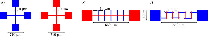
We identify two contributions to the resistance between two metal layers: an edge resistance resulting from the reduced cross-section of the metal layer at the transition to the overlap contact, and a contact resistance between two aluminum layers fabricated in separate lithographic steps. In order to be able to extract , we perform a four probe measurement on a set of four test patterns. Figure 5 shows schematic drawings of the four patterns, where layer 1 is drawn in blue and layer 2 is drawn in red. At first, we measure the sheet resistance of both aluminum thin films (see Fig. 5a). Here, the superscript corresponds to the respective number of the layer. Multiple measurements show very similar values for of both films. Measuring the DC resistance of the structure sketched in Fig. 5b allows to calculate the edge resistance by the following equation,
| (2) |
where is the number of squares of the red layer. From measurements on different samples we extract an upper bound for the edge resistance of . Knowing and allows to calculate with the equation below,
| (3) |
Calculation of the residual resistance
Based on the average of samples with argon ion milled contacts and a bridge (see Fig. 3b), we extract an upper bound on the residual resistance of the contacts. For the calculation we assume that all dissipation is caused by inductive loss, since the bridge and contacts are at a position of small electric and high magnetic field. The quality factor of a lossy inductor is defined as . Here, corresponds to the frequency, to the total inductance, and to the resistance of the inductor.
We estimate the total inductance by calculating the geometric inductance of a microstrip with a width of and a total length of , and taking into account the kinetic inductance fraction (see Fig. 4). For a frequency we calculate the residual resistance to be
| (4) |
Since all resonators with a bridge have two contacts, we divide the total resistance by two and then multiply by the area of one argon ion milled contact. This gives a residual resistance of one overlap contact of,
| (5) |
which we round up to to quote a conservative upper bound in the main text.
Parameter list of resonators
| sample | -120 dBm | -130 dBm | -140 dBm | -150 dBm | -160 dBm | -170 dBm | ||
|---|---|---|---|---|---|---|---|---|
| A | 4.4774 | 9.7 | 8.3 | 6.0 | 4.2 | 3.4 | 2.7 | 2.3 |
| 4.5503 | 4.8 | 7.4 | 5.8 | 4.3 | 3.0 | 1.3 | 0.5 | |
| 4.6257 | 0.6 | The amplitude signal shows an asymmetric response, which is not | ||||||
| captured in our model. Therefore, no values for can be extracted | ||||||||
| 4.7035 | 0.9 | 3.2 | 2.7 | 2.3 | 1.9 | 1.6 | 0.8 | |
| B | 4.5128 | 11.9 | 13.7 | 10.4 | 6.4 | 2.8 | 1.3 | 0.9 |
| 4.5872 | 2.6 | 8.7 | 7.7 | 5.5 | 3.6 | 2.0 | 1.5 | |
| 4.6649 | 0.7 | Not converging111The amplitude response shows a slight asymmetry, that dominates at higher readout powers. For smaller powers this only influences the shape of the amplitude response of the resonator marginally and is therefore neglected. | 4.1 | 2.5 | 1.6 | 1.2 | ||
| 4.7474 | 1.2 | 4.9 | 4.0 | 3.2 | 2.3 | 1.9 | 1.0 | |
| C | 4.4811 | 7.3 | 11.3 | 8.8 | 6.6 | 4.2 | 3.4 | 1.6 |
| 4.5586 | 1.4 | 11.7 | 9.5 | 7.0 | 4.0 | 3.4 | 1.4 | |
| 4.6370 | 0.5 | 21.9 | 14.6 | 9.0 | 5.4 | 2.9 | 2.4 | |
| The meander of the fourth resonator was interrupted during fabrication. | ||||||||
| D | 4.5310 | 30.5 | 8.6 | 6.4 | 3.0 | 1.1 | Not converging222Due to the very weak coupling the resonator response exhibits a very poor signal to noise ratio at low readout powers | |
| 4.6050 | 4.4 | 3.9 | 3.3 | 2.4 | 1.2 | 0.8 | 0.5 | |
| 4.6839 | 0.2 | The amplitude response shows a peak instead of a dip, which is not | ||||||
| captured in our model. Therefore, no values for can be extracted | ||||||||
| 4.7646 | 0.9 | 1.5 | 1.3 | 1.2 | 1.0 | 0.8 | 0.5 | |
Sample shielding