Charge-spin correlation in van der Waals antiferromagenet NiPS3
Abstract
Strong charge-spin coupling is found in a layered transition-metal trichalcogenide NiPS3, a van der Waals antiferromagnet, from our study of the electronic structure using several experimental and theoretical tools: spectroscopic ellipsometry, x-ray absorption and photoemission spectroscopy, and density-functional calculations. NiPS3 displays an anomalous shift in the optical spectral weight at the magnetic ordering temperature, reflecting a strong coupling between the electronic and magnetic structures. X-ray absorption, photoemission and optical spectra support a self-doped ground state in NiPS3. Our work demonstrates that layered transition-metal trichalcogenide magnets are a useful candidate for the study of correlated-electron physics in two-dimensional magnetic material.
pacs:
71.20.-b, 75.50.Ee, 78.20.CiIt is a fundamental question of modern condensed matter physics how the three-dimensional (3D) physics that we are familiar with breaks down upon reducing the dimension. It is generally believed that in one-dimensional physical systems, dimensional fluctuations will become stronger and ultimately destroy any long-range order. However, the same question for two dimensions is nontrivial and extremely hard to solve.
For this goal of new physics, layered van der Waals (vdW) materials, such as graphene and transition metal (TM) dichalcogenides, have attracted much attention over the last decade 1 ; 2 ; 3 . A remarkable advantage of these materials is that they can easily be mechanically exfoliated to produce two-dimensional (2D) crystals 1 ; 2 ; 3 . The intriguing collective quantum phenomena found in 2D vdW materials include charge density waves and superconductivity 4 ; 5 ; 6 ; 7 ; 8 . These observations open a new window of opportunity for novel device applications through the manipulation of collective quantum states in atomically thin 2D phases 3 ; 6 ; 9 . Despite the extensive study of vdW materials, it is striking that there have been very few studies of magnetic 2D vdW materials.
Only recently has attention been focused on new magnetic 2D vdW materials of ternary transition-metal trichalcogenide (TMTC) families, such as CrBTe3 (B = Si or Ge) and TMPX3 (TM = 3d TMs; X = chalcogens) 10 ; 11 ; 12 . These TMTC bulk samples exhibit various magnetic orderings: ferromagnetic (FM), zig-zag antiferromagnetic (AF), Néel AF, and stripy AF 11 ; 12 . Moreover, all three key magnetic Hamiltonians, i.e., Ising, XY, and Heisenberg types, are realized in TMPX3 13 ; 14 ; 15 ; 16 . Of further interest, long-range magnetic ordering has recently been reported to persist even in the monolayer limit, e.g., FePS3 and CrGeTe3 10 ; 10-1 ; 14 . Thus, it has become clear that the TMTC families, i.e., the layered vdW magnets, are a fertile playground for exploring rich and intriguing phenomena related to 2D magnetism, which will ultimately pave the way to novel applications in spintronics.
Compared with other nonmagnetic vdW materials, these new magnetic vdW materials offer another distinct and fundamental opportunity, namely insight into strongly correlated electronic systems in the 2D limit. Over the past few decades, researchers have attempted to unravel correlation physics using 2D materials 17 ; 18 ; 19 ; e.g., oxide ultrathin films produced by pulsed laser deposition (PLD) and molecular beam epitaxy (MBE), where a variety of emergent phenomena are reported to take place 21 ; 22 . With magnetism being an intrinsic property of TMTC, it is natural for us to expect to see some correlation physics, even in the 2D limit of those materials. It is well-known that in magnetic TM oxides, electron-electron correlation plays a central role in magnetic interactions, including superexchange and double exchange mechanisms 25 ; 24 . For instance, many 3d TM oxides exhibit AF ordering as a consequence of the superexchange processes associated with d-d hopping, whose amplitude is directly related to the correlation interaction energy. To date, the electron correlation effects in TMTC remain largely unexplored experimentally, despite their potential importance.
In this Letter, we report on the electronic structure of bulk NiPS3 single crystal, a TMTC antiferromagnet in which the electronic and spin (or magnetic) structures are closely related to one another. Using optical spectroscopy techniques we observed clear anomalies in the optical spectral weight at the Néel temperature, driven mainly by the magnetic ordering, which is a hallmark of correlated electronic systems 26 ; 27 . Subsequent x-ray absorption and photoemission studies also showed, together with cluster model calculations, that NiPS3 is a self-doped negative charge transfer (NCT) insulator. That is, the ligand (sulfur atoms) has a strong hole-like character due to a NCT energy, unlike more conventional systems. Such an intriguing electronic and magnetic ground state was also confirmed by density functional theory (DFT) with Coulomb interaction (U) calculations. Our studies identify NiPS3 as a unique vdW magnet showing clear evidence of strong correlation and NCT behavior.
High-quality single crystals of NiPS3 were grown by a chemical vapor transport method, as described in Ref. 28 ; 28-1 . For the optical measurements, we used a 55-m-thick single crystal sample and an M-2000 ellipsometer (J. A. Woollam Co.). In addition, we carried out the DFT+U calculations using the Quantum Espresso package 31 ; 32 ; 33 ; 34 ; 35 ; 36 ; 37 ; 38 (for details on the DFT method, see Supplemental Materials (a-1) 30 ).
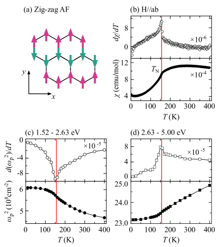
NiPS3 is one of the transition-metal phosphorous trichalcogenides (TMPX3) with an AF long-range ordering at 154 K. It has a monoclinic structure with C symmetry and features edge-sharing NiS6 octahedra arranged on a honeycomb lattice 28 ; 39 . At the center of the honeycomb lattice, two P atoms are located above and below the TM plane. They are then connected to the S atoms like a dumbbell, forming a (P2S6)4– bipyramid structure 39 ; 40 . It is known that the magnetic moments of Ni ions are aligned in a so-called “zig-zag” pattern; i.e., chains of ferromagnetically coupled spins are arranged antiferromagnetically, as shown in Fig. 1(a) 32 . Our in-plane magnetic susceptibility (T) shows an AF magnetic anomaly at the Néel temperature ( 154 K) [Fig. 1(b)].
The optical conductivity spectra ) show that NiPS3 is an insulator with an optical gap of about 1.8 eV [Fig. 2(a)]. At the same time, there are strong narrow absorption peaks in the visible-ultraviolet energy regions, near 2.2, 3.5, and 4.6 eV [labeled A, B, and C, respectively, in Fig. 2(a)]. Below the gap, there exists two additional weak peaks near 1.1 and 1.7 eV denoted as and , respectively [see the inset of Fig. 2(a)]. For comparison, NiO, which has the same formal valence of Ni (+2) as NiPS3, is reported to have weak on-site d-d transitions at 1.13 and 1.75 eV 41 . Due to the similarities in the energy positions and strengths of the peaks, it is most likely that the and peaks are the on-site d-d transitions, a transition within one Ni ion. It should be noted that the hybridization of Ni 3d orbitals with S 3p can provide a much larger bandwidth than that with O 2p in NiO. Nonetheless, the narrowness of the A, B, and C peaks, in addition to the existence of the and peaks, suggest the presence of well-localized Ni 3d orbital states near the Fermi surface (EF) in the electronic structure.
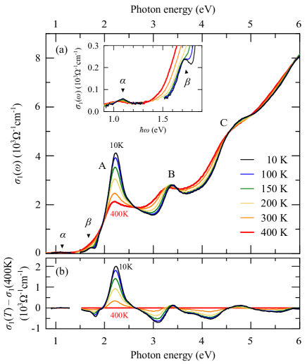
When we measure the temperature dependence of the optical conductivity of NiPS3, it displays strong temperature variations. For example, Fig. 2(b) shows the difference curve of ) at various temperatures after subtracting off the 400 K spectrum. Note that peak A shows strong enhancement in intensity while peaks B and C sharpen without much change in intensity upon cooling. To quantify the temperature evolution, we calculated the squares of the plasma frequency : = 42 , which we refer to as the spectral weight (SW). The optical sum rule is satisfied when we integrate up to 4.2 eV, implying the clear SW shifts from peak A to peaks B and C (see Supplemental Materials (b) 30 ). At the same time, satisfaction of the optical sum rule indicates that most of the temperature-dependent changes in the electronic structure should occur near the Fermi level, EF.
When we further examined the temperature dependence, we found clear anomalies in the SW changes of the main peaks occurring at TN. Figures 1(c) and 1(d) show the SW changes in the energy ranges of 1.52–2.63 eV and of 2.63–5.00 eV, respectively. The former represents the SW changes of peak A, and the latter represents those of peaks B and C. The lower panel of Fig. 1(c) shows that the (T) of peak A increased with decreasing temperature, with a kink structure at EF. The anomaly was seen more clearly in the first derivative of , as plotted on the upper panel. A similar feature was also observed in the temperature evolution of the SW of peaks B and C, as shown in Fig. 1(d). Thus, the observation of SW anomalies at EF constitutes the compelling evidence of strong coupling between the electronic and spin structures in NiPS3.
Conventionally, most ground states of strongly correlated compounds can be categorized via the Zaanen-Sawatzky-Allen (ZSA) classification scheme 43 ; 44 . Depending on the relative size of on-site U and charge-transfer energy (), the insulating ground state can be classified as either Mott-Hubbard or charge transfer insulators. In the former, the lowest energy charge fluctuation occurs between inter-site TM ions (dndn) (dn+1dn-1) with an energy cost of U, and in the latter, between ligand and TM ions (dnp6 dn+1p5) with (see Supplemental Materials (d) 30 ). However, there is a less-explored region in the ZSA scheme, where compounds can have NCT energy ( 0). In this region, electrons of the ligand p-orbital transfer to the TM d levels in the ground state, creating holes at the ligands without external doping. Because of this, they are often referred to as “self-doped” 45 . The ligand hole can naturally make an important contribution to the conductivity and magnetism 46 . To some extent, the nature of the self-doped state is analogous to the ground state of the Zhang-Rice singlet states found in hole-doped cuprates 47 ; 48 .
Indeed, this interpretation of the self-doped ground state agrees with XAS and XPS results of NiPS3. We obtained the Ni L2,3 edge XAS spectra of bulk NiPS3 which was subsequently analyzed using a cluster model (see Supplemental Materials (e-2) 30 ). At the L3 edge, NiPS3 show a main peak near 851 eV, which are clearly distinguished from that of compounds with large positive values, such as NiO ( 4.6 eV) or NiCl2 ( 3.6 eV), where the main peak shows clear splitting 49 . We simulated the Ni L2,3 edge XAS spectra using cluster model and found the NiPS3 belongs to the regime of 0 eV (see Supplemental Materials (e-3) [30]). In addition, the Ni 2p3/2 core XPS spectrum is found to be nearly identical to that of NiGa2S4, a first reported NCT sulfide 50 ; 55 (see Supplemental Materials (e-2) 30 ). The NiS6 cluster model used on NiGa2S4 also reproduces the Ni 2p3/2 XPS spectrum of NiPS3 well, using the parameters of = –1.0 and U = 5.0 eV. Note the calculated ground state is given as , where L indicates a ligand (sulfur) hole, with = 0.25, = 0.60 and = 0.15. Above findings support NiPS3 should have a self-doped ground state with dominant character, and demonstrate NiPS3 as the only known example of a magnetically ordered vdW material with an NCT insulating state.
To gain further insight, we performed DFT+U calculations. We used a magnetic ground state with a zig-zag AF ordering [Fig. 1(a)] and an effective U value of 4 eV. The solid line in Fig. 3(a) shows the theoretical calculation of in-plane ) after rescaling the data, in a way that satisfies the sum rule, to match the energy position of the first transition peak (see Supplemental Materials (a-2) 30 ). The theoretical ) reproduced most of the key features found in our experimental data.
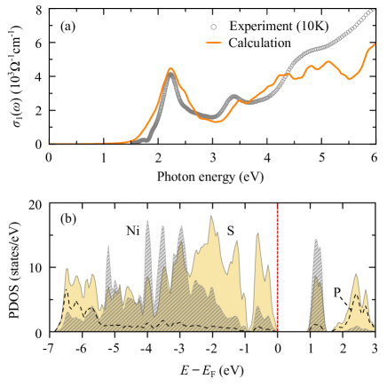
The DFT+U calculations also support our interpretation of the self-doped NCT ground state for NiPS3. Figure 3(b) shows the projected density of states (PDOS) for Ni, P, and S orbitals in NiPS3; as shown by the dashed curve, the P 3p states are located mostly above 2 eV or below –5 eV, and show a strong hybridization with the S 3p orbitals as a result of covalent bonding in the P2S6 bipyramids 39 ; 40 . On the other hand, the PDOS for Ni and S orbitals is much higher near EF than that of P 3p [Fig. 3(b)]. Thus, the valence bands near EF are mainly S 3p orbital states, and the occupied Ni 3d orbital states are located mostly at lower energies. Narrow Ni 3d bands hybridized with the S 3p show up at 1.3 eV above EF. The S 3p orbitals are located at higher energies than most Ni d orbitals, which indicates charge transfer from S to Ni ions in the ground state, and is consistent with the NCT picture 46 . Thus, the ground state is expected to have strong contributions from and configurations, in addition to .
The total number of d-electrons from the PDOS analysis of our DFT+U was larger than expected from the formal valence, which is consistent with a self-doped NCT ground state. While Ni2+ ion in the formal valence is expected to have an occupation number of 8, we obtained 8.6 from our PDOS analysis. Such an increase in the occupation number was also found in a DFT study of Cs2Au2Cl6, which showed a larger occupation number of d-electrons than expected from the formal valence because 0 56 .
The picture of the self-doped ground state also finds support from the magnetic properties. According to our DFT+U calculations, the theoretical value of the ordered magnetic moment is 1.24 per Ni ions, as opposed to the formal value of 2 . This reduction in the magnetic moment can be easily understood using the results of our cluster calculations. As mentioned earlier, the ground state consists of three configurations, each with different spin numbers: (SNi = 1), (SNi = 1/2), and (SNi = 0). In addition, our calculations show that four S ions in each NiS6 octahedron have spin polarizations (0.15 ) aligned in the same direction as the spin of the central Ni ion. The remaining S positioned in the middle of two adjacent FM chains, as well as the P ions, are nonmagnetic (see Supplemental Materials (a-3) 30 ). Here, we would like to point out that a recent neutron diffraction experiment on NiPS3 also reported a large reduction in the Ni moment with an experimental ordered moment of 1.05 32 . We speculate that this reduction in the magnetic moment of Ni ions, consistently supported by our theory and experiment, is a natural consequence of the charge transfer energy being negative.
Let us revisit the temperature-dependent SW anomaly, shown in Figs. 1(c) and 1(d), within the simple cluster picture. In the state, the lowest energy transition, peak A, is expected to be enhanced when the neighboring Ni ions are bonded antiferromagnetically. The corresponding ground state should be composed of t2g6eg3 electrons at Ni 3d orbitals and one hole at S 3p orbitals (); i.e., t2g6eg3, with the 3A2g symmetry 50 (see Supplemental Materials (f) 30 ). According to the NiS6 cluster model, the lowest-energy ionization state was found to have 2Eg symmetry 50 ; 57 , and the corresponding state is clearly seen in XPS valence spectra (see Supplemental Materials (e-4) 30 ). This suggests that peak A could be assigned as an inter-site transition between NiS6 clusters that transfer an electron between two t2g6eg3 (3A2g) clusters. These transitions would split the ground state into a low spin t2g6eg2/t2g6eg32 state on one site and a low spin t2g6eg3/t2g6eg4 state on the other site. Considering spin conservation, such transitions may be allowed between AF-bonded clusters, but forbidden between FM-bonded clusters.
Therefore, the temperature-dependent SW and its anomaly should arise from the increased AF bonds in zig-zag-ordered honeycomb lattice. At the temperature above TN, there will be no preference between AF and FM bonds of NiS6 clusters. Below TN, however, the number of AF and FM bonds will differ: For the nearest neighboring Ni ions (with exchange interaction J1), there will be 2 FM and a AF bonds; for the second-nearest (J2), 2 FM and 4 AF bonds; and for the third-nearest (J3), 3 AF bonds only. Recent calculations on the monolayer of the NiPS3 predicted that J3 is nearly four times larger than J1, while the value of J2 is very small 58 ; 59 . Likewise, the dominant strength of J3 is consistent with the increased number of AF bonds below TN, and consequently the increased intensity of peak A. The SW, therefore, should reflect the degree of AF correlation present at a given temperature, which is consistent with SW anomalies observed across TN in the experiments [Fig. 1(c)].
In summary, we investigated the electronic structures of NiPS3, one of the layered vdW antiferromagnets. Our results showed strong charge-spin coupling; i.e., a close relationship between the electronic structure and the magnetic ordering. We also found that NiPS3 is a rare self-doped NCT insulator; i.e., a strong hole-character is present in the ground state. Our findings provide a basis to explore a novel material class of vdW magnets, which could lead to rich and intriguing phenomena related to 2D magnetism and enable new applications in novel spintronic devices.
Acknowledgements.
We gratefully acknowledge insightful discussions with K. W. Kim, K. Burch and B. C. Park. This work was supported by Institute for Basic Science (IBS) in Korea (Grant No. IBS-R009-D1, IBS-R009-G1). S. J. Moon was supported by Basic Science Research Program through the National Research Foundation of Korea (NRF) funded by the Ministry of Science, ICT and Future Planning (Grant No. 2014R1A2A1A11054351 and 2017R1A2B4009413). T. Y. Kim and C. -H. Park were supported by Korean NRF-2016R1A1A1A05919979. Experiments at PLS-II were supported in part by MSIP and POSTECH. The STXM experiment was supported by the National Council of Science & Technology grant (Grant No. CAP-16-01-KIST and NRF-2016K1A3A7A09005335). W. Kim specially thanks to N. Kim and H. Shin for their supporting for STXM measurement at PLS-II.E-mail address:
*soonjmoon@hanyang.ac.kr
†twnoh@snu.ac.kr
‡jgpark10@snu.ac.kr
References
- (1) K. S. Novoselov, D. Jiang, F. Schedin, T. J. Booth, V. V Khotkevich, S. V Morozov, and A. K. Geim, Proc. Natl. Acad. Sci. 102, 10451 (2005).
- (2) K. S. Novoselov, A. K. Geim, S. V. Morozov, D. Jiang, Y. Zhang, S. V. Dubonos, I. V. Grigorieva, and A. A. Firsov, Scinece 306, 666 (2004).
- (3) A. K. Geim, and I. V Grigorieva, Nature 499, 419 (2014).
- (4) X. Xi, L. Zhao, Z. Wang, H. Berger, L. Forró, J. Shan, and K. F. Mak Nat. Nanotechnol. 10, 765 (2015).
- (5) K. F. Mak, K. He, J. Shan, and T. F. Heinz, Nat. Nanotechnol. 7, 496 (2012).
- (6) K. S. Novoselov, A. Mishchenko, A. Carvalho, and A. H. Castro Neto, Science 353, 461 (2016).
- (7) M. V. Sadavskii, Physics-Uspekhi 59, 947 (2016).
- (8) A. H. Castro Neto, Phys. Rev. Lett. 86, 4382 (2001).
- (9) X. Li and J. Yang, Natl. Sci. Rev. 3, 365 (2016).
- (10) C. Gong, L. Li, Z. Li, H. Ji, A. Stern, Y. Xia, T. Cao, C. Wang, Y. Wang, Z. Q. Qiu, R. J. Cava, S. G. Louie, and J. Xia, Nature 546, 265 (2017).
- (11) Additionally, the ferromagnetism in monolayer was reported in CrI3 compound; see Bevin Huang, Genevieve Clark, Efrén Navarro-Moratalla, Dahlia R. Klein, Ran Cheng, Kyle L. Seyler, Ding Zhong, Emma Schmidgall, Michael A. McGuire, David H. Cobden, Wang Yao, Di Xiao, Pablo Jarillo-Herrero, and Xiaodong Xu, Nature 546, 270 (2017).
- (12) N. Sivadas, M. W. Daniels, R. H. Swendsen, S. Okamoto, and D. Xiao, Phys. Rev. B 91, 235425 (2015).
- (13) B. L. Chittari, Y. Park, D. Lee, M. Han, and A. H. Macdonald, Phys. Rev. B 94, 184428 (2016).
- (14) A. R. Wildes, K. C. Rule, R. I. Bewley, M. Enderle, and T. J. Hicks, J. Phys. Condens. Matter 24, 416004 (2012).
- (15) J.-U. Lee, S. Lee, J. H. Ryoo, S. Kang, T. Y. Kim, P. Kim, C.-H. Park, J. Park, and H. Cheong, Nano Lett. 16, 7433 (2016).
- (16) A. R. Wildes, B. Roessli, B. Lebech, and K. W. Godfrey, J. Phys. Condens. Matter 10, 6417 (1998).
- (17) J. Park, J. Phys. Condens. Matter 28, 301001 (2016).
- (18) D. Neilson, A. Perali, and M. Zarenia, J. Phys. Conf. Ser 702, 012008 (2016) .
- (19) J. Sabio, J. Nilsson, and A. H. Castro Neto, Phys. Rev. B 78, 075410 (2008).
- (20) J. Crossno, J. K. Shi, K. Wang, X. Liu, A. Harzheim, A. Lucas, S. Sachdev, P. Kim, T. Taniguchi, K. Watanebe, T. A. Ohki, and K. C. Fong, Science 351, 1058 (2016).
- (21) J. H. Ngai, F. J. Walker, and C. H. Ahn, Annu. Rev. Mater. Res. 44, 1 (2014).
- (22) P. Zubko, S. Gariglio, M. Gabay, P. Ghosez, and J.-M. Triscone, Annu. Rev. Condens. Matter Phys. 2, 141 (2011).
- (23) D. I. Khomskii, Basic Aspects of the Quantum Theory of Solids (Cambridge University Press, New York, 2010).
- (24) D. I. Khomskii, Transition Metal Compounds (Cambridge University Press, New York, 2014), 1st ed..
- (25) D. N. Basov, R. D. Averitt, D. Van Der Marel, M. Dressel, and K. Haule, Rev. Mod. Phys. 83, 471 (2011).
- (26) Millis, A. J., Optical Conductivity and Correlated Electron Physics, edited by D. Baeriswyl and L. Degiorgi, Strong Interactions in Low Dimensions, (Kluwer Academic Publishers, Dordrecht, 2004), pp. 195-236.
- (27) C. T. Kuo, M. Neumann, K. Balamurugan, H. J. Park, S. Kang, H. W. Shiu, J. H. Kang, B. H. Hong, M. Han, T. W. Noh, and J. G. Park, Sci. Rep. 6, 20904 (2016).
- (28) We subsequently checked the stoichiometry using a scanning electron microscope (COXI EM30; COXEM), equipped with an energy-dispersive x-ray spectrometer (Bruker Quantax 100), which was followed by magnetic susceptibility measurements obtained with a SQUID-VSM (MPMS 3; Quantum Design).
- (29) E. Stavitski and F. M. F. de Groot, Micron 41, 687 (2010).
- (30) See Supplemental Materials
- (31) S. L. Dudarev, G. A. Botton, S. Y. Savrasov, C. J. Humphreys, and A. P. Sutton, Phys. Rev. B 57, 1505 (1998).
- (32) A. R. Wildes, V. Simonet, E. Ressouche, G. J. McIntyre, M. Avdeev, E. Suard, S. A. J. Kimber, D. Lançon, G. Pepe, B. Moubaraki, and T. J. Hicks, Phys. Rev. B 92, 224408 (2015).
- (33) D. R. Hamann, Phys. Rev. B 88, 85117 (2013).
- (34) M. Schlipf and F. Gygi, Comput. Phys. Commun. 196, 36 (2015).
- (35) J. P. Perdew, K. Burke, and M. Ernzerhof, Phys. Rev. Lett. 77, 3865 (1996).
- (36) A. Marini, C. Hogan, M. Gruning, and D. Varsano, Comput. Phys. Commun. 180, 1392 (1996).
- (37) Z. H. Levine and D. C. Allen, Phys. Rev. B 63, 1719 (1996).
- (38) P. Giannozzi, S. Baroni, N. Bonini, M. Calandra, R. Car, C. Cavazzoni, D. Ceresoli, G. L. Chiarotti, M. Cococcioni, I. Dabo, A. D. Corso, S. Fabris, G. Fratesi, S. de Gironcoli, R. Gebauer, U. Gerstmann, C. Gougoussis, A. Kokalj, M. Lazzeri, L. Martin-Samos, N. Marzari, F. Mauri, R. Mazzarello, S. Paolini, A. Pasquarello, L. Paulatto, C. Sbraccia, S. Scandolo, G. Sclauzero, A. P. Seitsonen, A. Smogunov, P. Umari, and R. M. Wentzcovitch, J. Phys. Condens. Matter 21, 395502 (2009).
- (39) R. Brec, Solid State Ionics 22, 3 (1986).
- (40) M. Piacentini, V. Grasso, S. Santangelo, M. Fanfoni, S. Modesti, and A. Savoia, Solid State Commun. 51, 467 (1984).
- (41) R. Newman and R. Chrenko, Phys. Rev. 114, 1507 (1959).
- (42) M. Dressel and G. Gruner, Electrodynamics of Solids: Optical Properties of Electrons in Matter (Cambridge University Press, New Yok, 2002).
- (43) J. Zaanen, G. A. Sawatzky, and J. W. Allen, Phys. Rev. Lett. 55, 418 (1985).
- (44) A. E. Bocquet, T. Mizokawa, T. Saitoh, H. Namatame, and A. Fujimori, Phys. Rev. B 46, 3771 (1992).
- (45) M. A. Korotin, V. I. Anisimov, D. I. Khomskii, and G. A. Sawatzky, Phys. Rev. Lett. 80, 4305 (1998).
- (46) G. Sawatzky, R. Green, J. van den Brink, E. Koch, and E. Pavarini, The Explicit Role of Anion States in High-Valence Metal Oxides, Modeling and Simulation 6, 420 (2016).
- (47) C. Monney, V. Bisogni, K. J. Zhou, R. Kraus, V. N. Strocov, G. Behr, S. L. Drechsler, H. Rosner, S. Johnston, J. Geck, and T. Schmitt, Phys. Rev. B 94, 165118 (2016).
- (48) D. Choudhury, P. Rivero, D. Meyers, X. Liu, Y. Cao, S. Middey, M. J. Whitaker, S. Barraza-Lopez, J. W. Freeland, M. Greenblatt, and J. Chakhalian, Phys. Rev. B 92, 201108 (2015).
- (49) G. van der Laan, J. Zaanen, G. A. Sawatzky, R. Karnatak, and J.-M. Esteva, Phys. Rev. B 33, 4253 (1986).
- (50) K. Takubo, T. Mizokawa, J. Y. Son, Y. Nambu, S. Nakatsuji, and Y. Maeno, Phys. Rev. Lett. 99, 037203 (2007).
- (51) S. Nakatsuji, Y. Nambu, H. Tonomura, O. Sakai, S. Jonas, C. Broholm, H. Tsunetsugu, Y. Qiu, and Y. Maeno, Science 309, 1697 (2005).
- (52) J. P. Perdew, Int. J. Quantum Chem. 28, 497 (1985).
- (53) X. Li, T. Cao, Q. Niu, J. Shi, and J. Feng, Proc. Natl. Acad. Sci. 110, 3738 (2013).
- (54) M. Bernasconi, G. L. Marra, G. Benedek, L. Miglio, M. Jouanne, C. Julien, M. Scagliotti, and M. Balkanski, Phys. Rev. B 38, 12089 (1988).
- (55) It seems that the lower electronegativity of chalcogen ions in TMTC can also drive the system into NCT regime, as in the cases of some TM oxides 45 ; 44 ; 46 ; 47 .
- (56) A. V Ushakov, S. V Streltsov, and D. I. Khomskii, J. Phys. Condens. Matter 23, 445601 (2011).
- (57) K. Takubo, T. Mizokawa, Y. Nambu, and S. Nakatsuji, Phys. Rev. B 79, 134422 (2009).
- (58) B. L. Chittari, Y. Park, D. Lee, M. Han, A. H. MacDonald, E. Hwang, and J. Jung, Phys. Rev. B 94, 184428 (2016).
- (59) The calculated exchange interaction strength value of bulk NiPS3 in our work also gave similar results for J1, J2 and J3 as in the monolayer case 58 .