Electron spin inversion in fluorinated graphene nanoribbons
Abstract
We consider a dilute fluorinated graphene nanoribbon as a spin-active element. The fluorine adatoms introduce a local spin-orbit Rashba interaction that induces spin-precession for electron passing by. The spin precession involving a single adatom is infinitesimal and accumulation of the spin precession events with many electron passages under adatoms is necessary to accomplish a spin flip. In order to arrange for this accumulation a circular n-p junction can be introduced to the ribbon by e.g. potential of the tip of an atomic force microscope. Alternatively a fluorinated quantum ring can be attached to the ribbon. We demonstrate that the spin-flip probability can be increased in this manner by as much as three orders of magnitude. The Zeeman interaction introduces spin-dependence of the Fermi wave vectors which changes the electron paths within the disordered system depending on the spin orientation. The effect destroys the accumulation of the spin precession events in the n-p junction. For side attached quantum rings however - for which the electron path is determined by the confinement within the channel – the accumulation of the spin precession is robust against the Zeeman spin splitting.
I Introduction
The coherent spin transport in semiconducting materials fabian is under extensive studies since the idea for the spin transistor was introduced datta . Graphene castro due to the absence of hyperfine interactions and long spin coherence times han ; maassen is a good candidate for a spin conductor. However, pristine graphene is a poor material for spin-active elements due to the weakness of the spin-orbit interaction manchon ; laird . Enhancement of the spin-orbit coupling was proposed by deposition of graphene on transition metal dichalcogenides (TMDC) avsar ; gmitra . The coupling with the TMDC layer gives rise to a strong Rashba interaction gmitra that accompany redistribution of the electron charge density and an appearance of the electric field component perpendicular to the graphene plane. Alternatively, the spin-orbit interaction can be introduced by adatoms kotov , hydrogen hy1 ; hy2 ; hy3 ; hy4 ; hy5 ; hy6 ; hy7 or fluorine fl1 ; fl2 ; fl3 ; fl4 ; fl5 ; fl6 ; irmer2015 . The latter is ten times more efficient than the former as the source of the spin-orbit coupling irmer2015 .
In this paper we consider transport across the graphene nanoribbon waha with a dilute fluorinated segment as a spin inverter of the Fermi level electrons that could be implemented as a spin transistor channel datta . The procedure to detect the spin flips on the electron motion within the spin-orbit coupled medium was recently demonstrated chuang . The system chuang employs two quantum point contacts which are transparent to a single spin direction only. The rotation of the electron spin on the way from one contact to the other results in the conductance drop.
We study the effects of the spin precession induced by the Rashba interaction near the adatoms. We find that in the absence of the external magnetic field the spin-flip probability is very low, which we attribute to cancellation of the spin precession effects by multiple electron backscattering since the direction of the spin precession in the Rashba field depends on the orientation of the electron momentum datta .
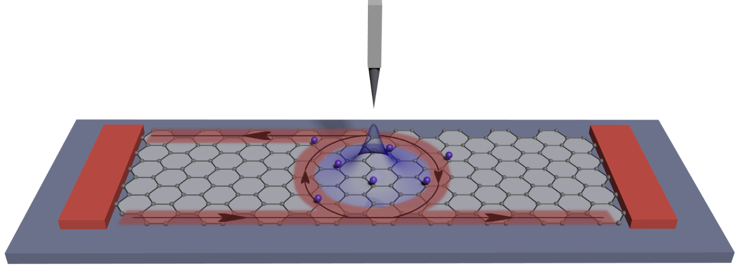
In order to strengthen the spin-orbit coupling effects we introduce an n-p junction in an external magnetic field. The n-p junctions in graphene can be induced by electrostatic potential which moves the Dirac point above or below the Fermi level castro . In the quantum Hall conditions these junctions form waveguides that confine currents wg1 ; wg2 ; wg3 ; wg5 ; wg4 ; wgx ; wg11 ; wgk . The confinement in the classical terms can be understood as a result of the Lorentz force pushing the electrons to the n-p junction at both its sides. The opposite orientation of the Lorentz force for the carriers of the conduction and valence band in classical terms produces snake-orbits wg4 ; wgx ; wg8 ; wg9 ; wg6 ; wg7 ; wg10 ; wg12 ; wgk winding along the junction. The magnetic confinement of the current along the junction is supported for a single direction of the current only. The effects of the spin-precession by the local Rashba interaction can be accumulated provided that the Fermi level electron passes many times under adatoms with weak backscattering. In order to recycle the electron passages we consider a circular n-p junction defined by e.g. an external gate of the scanning probe microscope gorini ; bhanda ; tapa ; mre1 ; mre2 . In the quantum Hall conditions the current comes to the junction from the edge and the lifetime of the localized resonances with the current circulation around the ring can be controlled by the gate potential, the Fermi energy mre1 and the external magnetic field mre2 . We find that for the current circulating around the junction the spin-flip probability on the electron transfer can be increased by as much as three orders of magnitude.
We also consider the fluorinated ribbon in the quantum Hall conditions with the external potential removed. In strong magnetic fields the localized resonances are associated with the current circulation from one adatom to the other and no backscattering along the path of incidence is possible. In these conditions for a number of magnetic field values the spin-flip probability produces high peaks. For low magnetic field we find a dip of conductance which is a signature of the weak localization effects that in graphene are present when the inter-valley scattering is strong wlg . In the present problem the adatoms as atomic scale perturbations to the lattice introduce strong intervalley scattering centers.
The effects of the accumulation of multiple spin flips requires that the electron trajectory remains unaffected by the spin orientation. The dependence of the trajectory within the disordered system on the spin orientation appears via the Zeeman interaction and the resulting spin dependence of the Fermi wave vector. In order to preserve large spin-flip probability the electron path across the fluorinated area needs to be weakly dependent on the wave vector. We show that this can be achieved with a fluorinated quantum ring side-attached to the ribbon. For one of the perpendicular magnetic field orientations the Fermi level wave function is injected to the ring provided that the Fermi energy is in resonance with states circulating within the ring mre2 . The resulting spin precession is stable against the spin Zeeman interaction. Quantum rings are defined in graphene ribbons with a well established by etching techniques qr1 ; qr2 ; qr3 ; qr4 ; szmel and the role o the magnetic focusing has been discussed recently mre2 ; szmel .
II Theory
II.1 Hamiltonian
We use the atomistic band tight-binding Hamiltonian, which in the absence of the fluorine adatoms takes the form
| (1) |
where and are the creation and annihilation operators for the electron on -th ion with spin . The first sum introduces the external potential at the position of the -th ion. The energy level corresponding to orbital is taken as the reference energy level. In the second summation runs over nearest neighbor carbon atoms and eV is the hopping parameter.
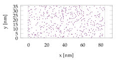
We consider a nanoribbon which in the absence of the adatoms is a strip of a crystal lattice of a finite width (see Fig. 1(a)). The experiments on graphene ribbons indicate a presence of the transport gap hantg ; chentg ; evaldtg near the charge neutrality point within which the system does not conduct electrical current. For that reason we consider here a semiconducting armchair ribbon. For the proof of principle in section III.A we take a ribbon that contains only 3 carbon atoms on its width. The rest of the results is obtained either for a thinner ribbon with 292 atoms across the width of nm (subsections III.B, III.C, III.D, and III.F) or for a wider ribbon (subsection III.E) with 1017 atoms across the width of nm. For the thinner (wider) ribbon the scattering region considered in this work is a central finite region 85.2 nm (127 nm) long with fluorine 400 (2165) adatoms in a dilute concentration. We also consider spin rotation within a fluorinated quantum ring of a circumference 283 nm [subsection III.F].
The locations of the fluorine atoms are generated at random with a uniform distribution. The results presented below are typical and quantitatively independent of the specific distribution. The position of the conductance peaks changes from one distribution to the other but the discussed physics does not. The fluorine atoms once adsorbed by graphene can only diffuse on its surface provided that the thermal excitations overcome migration barrier which for the fluorine adatoms is equal to 0.29 eV migratb . Therefore, the motion of the fluorine adatoms on the surface is frozen at low temperatures. The value changes with the carrier density level migratb2 , but below we consider mainly conditions of the lowest subband transport, i.e. low Fermi energies near the charge neutrality point.
A fluorine adatom [see Fig. 1(b)] introduces additional terms to the Hamiltonian irmer2015 ,
| (2) |
where stands for the orbital, and the spin-orbit coupling effects. The orbital contribution covers the level localized at the fluorine adatom () with the energy level eV and the hopping element eV between the fluorine and the carbon atom () that form a vertical dimer (, see Fig. 1(b)):
| (3) |
where is the annihilation operator for electron in the fluorine ion with spin , and is the annihilation operator for the fluorinated carbon atom.
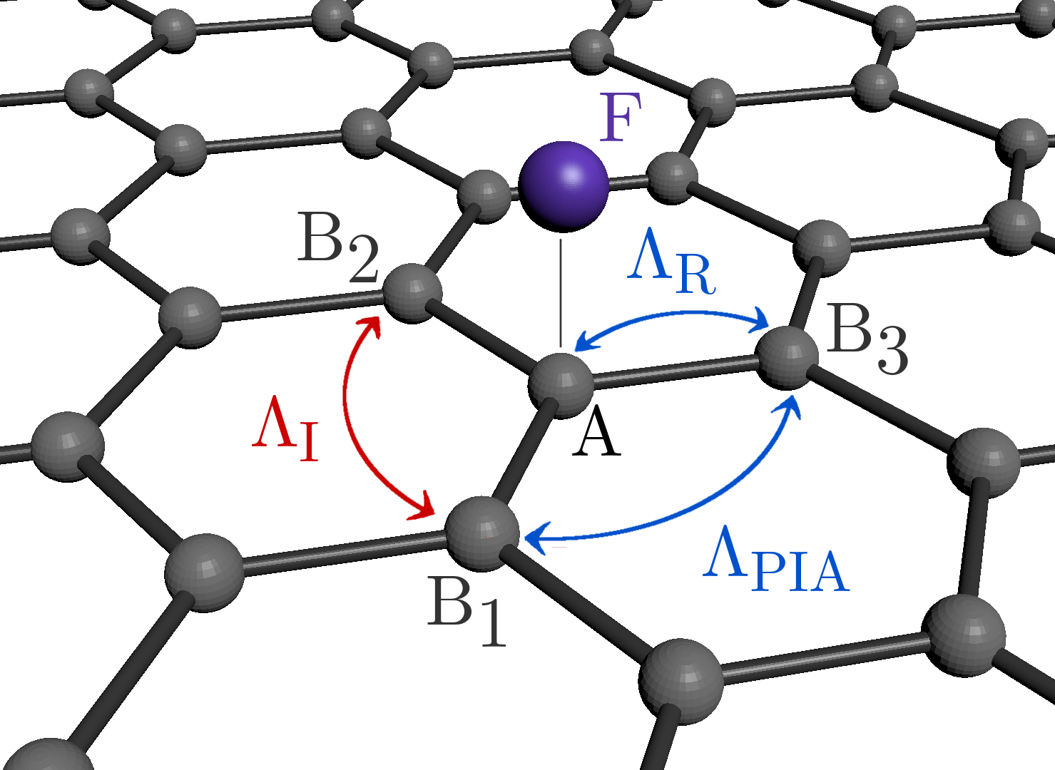
The three next nearest neighbor atoms of the fluorinated carbon are denoted by (see Fig. 1). The annihilation operator for the electron in the atoms is . With this notation the spin-orbital part has the form irmer2015
| (4) |
The first sum in the intrinsic spin-orbit coupling in the Kane-Mele form km which is spin-diagonal. The second term describes the Rashba interaction induced by the perpendicular electric field due to the deformation of the electron density by the adatom. The last term is the pseudospin-inversion-asymmetry next-nearest neighbor term that results from deformation of the graphene lattice by the adatom liu . The summation runs over the nearest neighbors of the fluorinated atom . The coefficient is () when the path from to via a common nearest neighbor , , is counterclockwise (clockwise) and is the unit vector in the plane oriented from ion to . The applied spin-orbit coupling parameters irmer2015 for concentration of the fluorine atoms are meV, meV and meV. Both the Rashba and the PIA terms induce spin variation in the electron motion across the fluorinated area. However, for the applied parameters the effect of the PIA is by an order of magnitude lower in terms of the spin-flipping transfer probability.
The orbital effects of the external perpendicular external magnetic field is introduced to the Hamiltonian by modification of the hopping parameters. For the Hamiltonian of Eq. (2) put in a general form,
| (5) |
in presence of the external magnetic field the hopping parameters are modified by the Peierls phase
| (6) |
where is the vector potential, is the magnetic flux quantum and is the position of -th ion.
The spin-effects of the magnetic field are introduced by the Zeeman interaction
| (7) |
with the Bohr magneton and .
II.2 Quantum rings: induced at the n-p junction and side-attached
In order to form an n-p junction within the ribbon we introduce an external potential of e.g. a charged tip of an atomic force microscope mre1 ; mre2 ; kolasinski2013 – see Fig. 2. The original tip potential is of the Coulomb form which is screened by deformation of the electron gas within the conducting plane. The Schrödinger-Poisson equations for the tip screened by the two-dimensional electron gas produce an effective tip potential kolasinski2013 which is close to the Lorentz form
| (8) |
where is the tip position over the plane, and is the effective width of the tip potential that is of the order of the tip-electron gas distance kolasinski2013 ), and depends on the charge accumulated by the tip. We adopt meV and nm as in the previous paper mre1 . In Hamiltonian given by Eq. (1), . For the workpoint we set meV with the fluorine concentration unless stated otherwise.
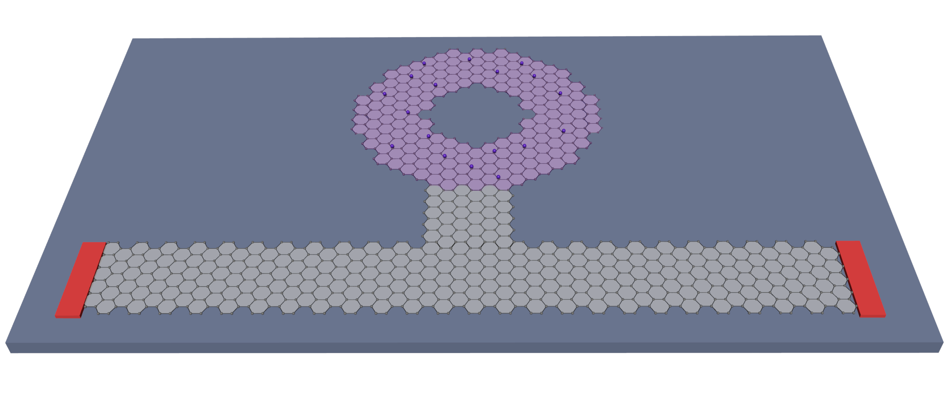
In presence of the Zeeman effect large spin-flips can be obtained when the electron path remains the same for both spin orientations. We arange for these conditions with a quantum ring side attached to the ribbon – see Fig. 3. The ribbon that is 293 atoms wide is considered for this purpose. The external and internal radii of the ring are 27 nm and 63 nm, respectively, and the arm of the ring contains about 293 atoms along its radius. The fluorine is adsorbed only within the ring.
II.3 Solution of the scattering problem
II.3.1 Implementation of the Landauer approach
Outside the scattering region the nanoribbon does not contain adatoms, so that the input and the output leads, i.e., the left and right ends of the ribbon, respectively, are free of the spin-orbit interaction. The eigenstates of the leads are spin-independent and are determined in the Bloch form
| (9) |
where is the wave vector for -th subband, numbers the elementary cells of the ribbons, and numbers the atoms inside the elementary cell. The wave function in the input lead is a superposition of the incident electron states with wave vectors and backscattered states with wave vectors ,
| (10) |
where the summation over runs over the subbands appearing at the Fermi level. At the output channel we have only the transferred, right-going waves
| (11) |
We solve for the scattering wave function that is an eigenstate of the Hamiltonian for an assumed Fermi energy that is glued to the boundary conditions given by Eqs. (10) and (11) for each incoming subband separately setting , for the electron incident from the subband . We use the wave function matching method wfmm , which produces the scattering amplitudes for the reflected () and transferred () waves.
For the Hamiltonian in form (6) the current flowing along the bonds between and ions is calculated as
| (12) |
where is the spin component of the wave function at the -th ion. The formula (12) accounts for the transfer of the current from one component of the spin to the other provided that the Hamiltonian contains the spin-orbit coupling components. This is indeed the case near the adatoms. Outside the fluorinated area the spin currents are conserved and can be calculated from Eq (12) for each component of .
We calculate the current fluxes outside the fluorinated area, at the ends of the ribbon which serve as the input and output leads,
| (13) |
where are the indices of the atoms across the ribbon and are their left (right) nearest neighbors in the ribbon left (right) lead where the flux is calculated. The electron transfer probability from the subband to the subband is calculated as
| (14) |
where and are the scattering amplitudes of the transferred wave function and incident wave functions, in the and modes, respectively. The overall transfer probability from the -th subband is , which is used in the Landauer formula for conductance
| (16) |
where is the flux quantum. In the following we set the incident electron spins and the Bloch functions in the leads as eigenstates of the operator. We calculate the spin conserving , , and spin flipping conductance contributions and by summation of with respect to the two spin orientations, where and stand for the eigenstates with eigenvalues -1 and +1, respectively.
II.3.2 Boundary conditions
Boundary conditions for left (input) and right (output) lead was calculated using Wave Function Matching (WFM) method wfmm . The Hamiltonian matrix for infinite ribbon that serves as the input or output lead to the scattering region can be put in form
| (17) |
where matrix is the Hamiltonian of single elementary cell , matrix describes connections between cells and . Matrices and are the size of where is the orbital number for the atom inside elementary cell (factor 2 arise from spinor splitting). For an ideal periodic infinite ribbon matrices and are identical, therefore the symbol will be omitted from this point. The eigenfunction of the Hamiltonian can be divided on eigenfunctions for each elementary cell
| (18) |
where is the vector of size ( orbitals for each spinor). The wave function satisfies the equation
| (19) |
Using Bloch form of the wave function (9) in substitution
where , we get
| (20) |
For equation (20) above can be written as
| (21) |
Described eigenproblem has solutions: left-going and right-going modes - decaying or propagating. It is straightforward to identify right and left going evanescent modes. The eigenvalue satisfies for right-going evanescent modes and for left-going evanescent modes. For the propagating modes of Bloch waves the eigenvalue satisfies , with real , hence . Then we look for values of for a given and determine the corresponding wave vectors and periodic functions .
II.3.3 Calculation of the scattering amplitudes
Transmission and reflection probabilities are calculated using scattering coefficients and , respectively. The scattering wave function in the left output lead takes the form
where the term with describes the incident electron and the sum stands for the superposition of the backscattered electron waves. We calculate the derivative of the wave function
| (22) |
from where we get the equation for the wave function outside the computational box
| (23) |
Using scalar product for the wave function in the first cell and the function we obtain
| (24) |
where denote the inner product in discrete form. Defining matrices , and the vector we can rewrite Eq. (24) in a matrix form
| (25) |
which satisfies
| (26) |
Using Eq. (26) in Eq. (24) we obtain the left boundary condition. For the right end ( cell) the wave function
| (27) |
Using similar approach to the right end of the computational box
| (28) |
from which we get the wave function outside the right side of the computational box
| (29) |
Using scalar product
| (30) |
we get
| (31) |
III Results and Discussion
III.1 Accumulation of the spin precession events
As a proof of principle for accumulation of the local spin precession evens we consider a narrow ribbon depicted in Fig. 4.
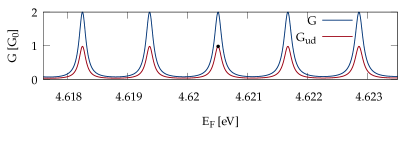
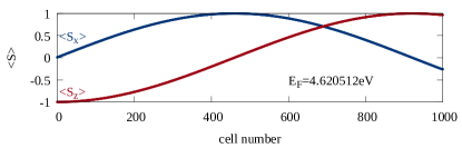
The ribbon is a sequence of hexagons with the fluorine atoms placed near the junctions of one hexagon to the other [Fig. 4]. No external magnetic field is applied and the electron is injected to the system with spin-down orientation from the left-hand side. The positions of the F atoms are repeated periodically within the ribbon, so the dependence on forms a series of resonances as for a superlattice band filter pacher . We set the value of the Fermi energy eV marked by the dot in Fig. 5 for which the system is transparent for electrons and look at the average spin and components calculated for subsequent hexagonal elementary cells of the ribbon in Fig. 6. For the resonant energy electron on its way across the system comes to fluorinated carbon atom with the same momentum and no backscattering is present. In total there are 400 atoms along the ribbon with the concentration . The overall conductance and the spin-flip contribution are depicted in Fig. 5.
Although an effect of a single fluorine atom to the orientation of the electron spin is very small we can see that upon transition below 400 fluorine atoms within the system which is nearly enough to rotate the electron spin from the the orientation. The source of the spin-flip transfer in the considered system is the Rashba component of the Hamiltonian that is due to the local electric field introduced by adatoms.
The Rashba spin-orbit interaction due to the adatom introduces an effective magnetic field meier meier , where is a constant, the electron momentum and the electric field vector. For the planar motion and the vertical electric field induced by the adatom, the is oriented along the direction, i.e. in-plane and perpendicular to the momentum orientation. The spin of the electron moving within the graphene layer precesses around datta ; chuang ; besza – in the case considered in Fig. 6 from the orientation to below the ribbon () through the orientation along the ribbon () for about 480th hexagonal cell of the ribbon to the orientation above the ribbon () for the 960th cell.

| (a) | |
|---|---|
| (b) | 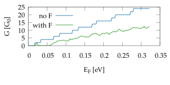 |
| (c) | 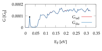 |
 |
III.2 Transport across a fluorinated layer at
The results of the preceeding subsection demonstrate that the spin flip is possible upon electron transition under many adatoms. Nevertheless, an experimental fabrication of the extremely narrow ribbon with ordered positions is rather unlikely. Let us then consider the ribbon which is 292 atoms wide with random locations of the atoms [see Fig. 1(a)].
The calculated electron transfer probability as a function of the Fermi energy is given in Fig. 7(a). The blue line indicates the ribbon conductance in the absence of the fluorine atoms, which in units is equal to the number of subbands that carry the flux to the right. The adatoms perturb the system and induce strong backscattering, which induces the drop of conductance in Fig. 7(a) with introduction of the adatoms. In the scattering region only 0.5% of the carbon atoms are fluorinated, but the perturbation of the potential by adatoms is strong and their random locations rule out the transparency of the system at resonances as in the ordered system of Fig. 5.
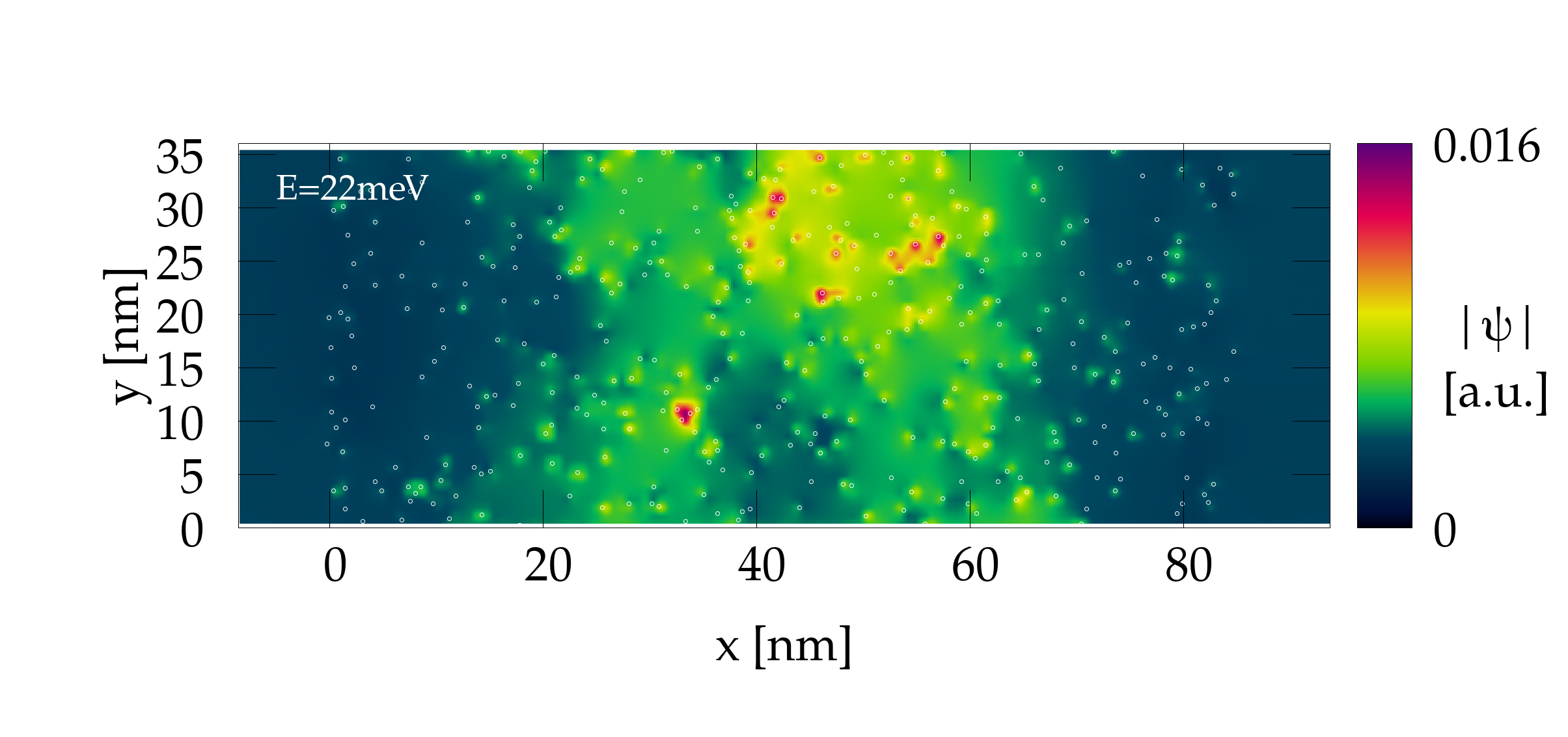
Only a very low spin-flip probability is observed [Fig. 7(b)]. A local maximum of the spin-flip probability near 0.022 eV [Fig. 7(b)] is associated with a quasi-bound resonance [Fig. 7(a)] that is supported by a group of adatoms [see the amplitude of the scattering wave function at Fig. 7(c)].
The electron backscattering by adatoms inverts the direction of the electron motion, and on the electron way back the spin precession besza due to the local Rashba interaction is reversed [see for the incident and for the backscattered motion in Fig. 8(a)], hence the near cancellation of the overall spin precession events that results in the low spin-flipping conductance contribution in Fig. 7(b).
Figure 7(b) shows that the spin-flipping effects of the electron passage across the fluorinated layer are very weak. Formation of a resonance supported by adatoms [Fig. 7(c)] with the Fermi electron experiencing a multiple scattering increases the electron dwelling time in the area where the spin-orbit coupling is present and enhances the spin-flip probability [see Fig. 7(b) near eV], which however remains very low.

III.3 Recycling the electron passages: circulation around n-p junction (Zeeman interaction neglected)
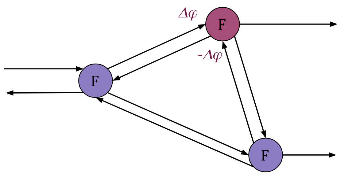
In order to accumulate the effects of the spin precession we introduced a n-p junction to the system defined by a gate potential – a tip of an atomic force microscope (see Fig. 2). In the perpendicular magnetic field, it is possible to induce long-living resonances localized at the n-p junction introduced by an external gate mre1 . Moreover, the electron backscattering along the same path as in Fig. 8(a) is no longer present in the quantum Hall conditions. The schematics of the current circulation in the quantum Hall conditions is given in Fig. 2. For the magnetic field oriented to the graphene plane the classical Lorentz force pushes the moving conduction band carriers to the right of their momentum. In consequence the incident and transfered current of conduction band electrons flows along the lower edge, while the backscattering mediated by the circular n-p junction goes through the upper edge. For the considered magnetic field orientation the current circulation around the n-p junction is clockwise (see Fig. 2), and the currents are stabilized for this single current orientation only mre2 . Formation of the waveguide at the n-p junction separated from the edge of the ribbon requires formation of the quantum Hall conditions. The separation of the edge and junction current occurs when a cyclotron radius fits between the edge and the junction. For the cyclotron orbit given by the magnetic length , the ribbon width and the diameter of the junction , the condition reads , which for the ribbon with 292 atoms considered here produces the condition T.
In this subsection we introduce external magnetic field with Hamiltonian . The spin Zeeman effect is introduced later.
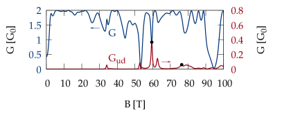
For the fluorine atoms present the conductance undergoes oscillations [Fig. 9] which are not as perfectly periodic as for the clean ribbon mre1 , nevertheless an approximate periodicity at higher can be noticed. The contribution to the conductance from the spin-flip transfer is – at higher magnetic field – large, reaching . Moreover, the spin flips – at higher – become periodic and correlated with the conductance maxima [cf. Fig. 9]. Note, that the maximal spin-flip transfer probability is increased by as much as three orders of magnitude with respect to Fig. 7(b).
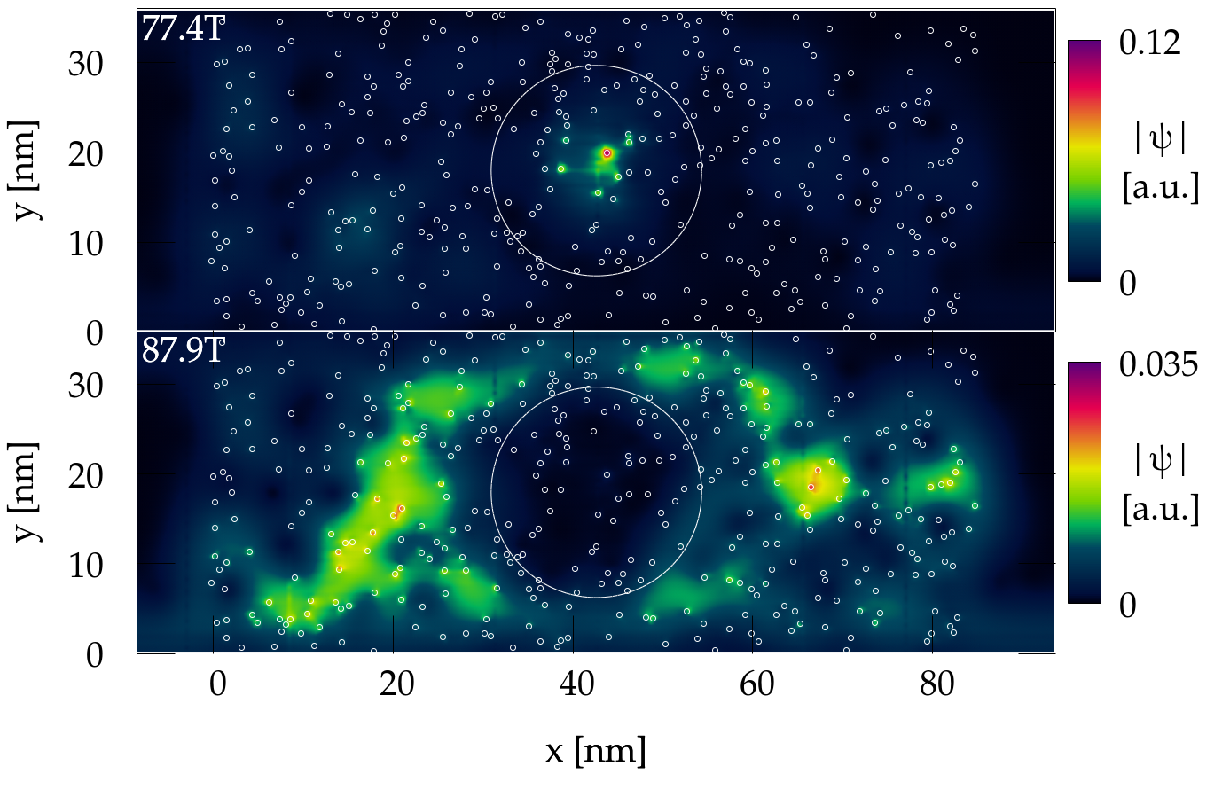
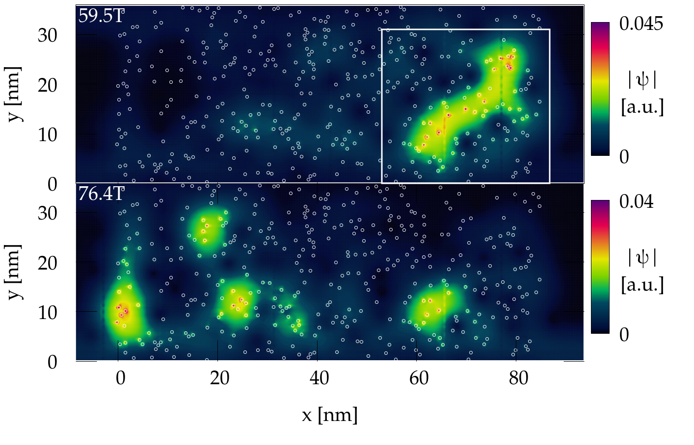
Figure 10 shows the scattering charge density at the carbon atoms for 77.4T and 87.9 T - for which the spin-flipping contribution to conductance presents local maxima [Fig. 9]. Figure 10(b) presents a typical scattering density distribution for the resonances encircling the n-p junction perturbed by the adatoms. In Fig. 10(a) a localization of the resonance at an adatom in the central – p conductivity – region can be seen. The resonances localized inside potential barrier were discussed in Ref. mre1, . Their long lifetime results from the direction of current circulation mre1 that the Lorentz force shifts to the center of the barrier and keeps the scattering density off the n-p junction.
Note, that the peaks of the overall conductance [Fig. 9(a)] and its spin-flipping contribution [Fig. 9(b)] are correlated already for T and the spin-flipping peaks increase in amplitude for higher . This results from an increasing magnetic confinement of the currents near the edge and the junction which decreases the coupling between the edge currents and the circular junction currents [Fig. 2] mre1 ; mre2 . The effect results in reduction of the coupling of the n-p junction to the edge. The lifetime of the resonances is increased along with the effects of the accumulation of the spin precession phase shifts.
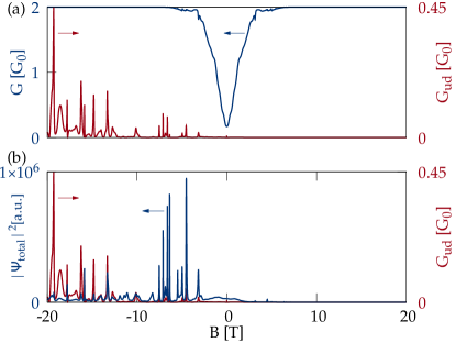
III.4 Resonances in the disordered sample (Zeeman interaction neglected)
The conductance with the external potential of the precedent section removed is plotted in Fig. 11. We observe an aperiodic dependence of conductance as a function of the external magnetic field. A conductance dip at [Fig. 12(a)] is characteristic to the weak localization as for a disordered conductor. In graphene the weak localization dip is observed when the intervalley scattering is strong wlg . In the present paper the role of the atomic scale defects that induce the intervalley scattering is played by the adatoms themselves. The intervalley scattering length can be estimated by the average distance between the atoms which is 1.5 nm for the dilute 0.5% F concentration. In the present paper we consider ideal edges of the ribbons. The defects of the edge introduce additional intervalley scattering in addition to the adatoms. When the edge is defected the peaks of conductance for nonzero change in position and the weak-localization dip varies in depth but the dependence is not qualitatively changed.
In perpendicular external magnetic field the resonances supported by the adatoms are also associated with current circulation from one scattering event to the other, and the backscattering along the same path which limits the spin precession effects does not occur [Fig. 8(b)] due to the Lorentz forces. This opens a chance for accumulation of the spin precession effects as for circular n-p junction. High peaks of the spin-flipping contribution to conductance are found [Fig. 12(b)] with irregular positions at the scale. The peaks of spin flipping conductance are now correlated with the dips of the spin-conserving conductance in contrast to the results obtained for the circular n-p junction discussed above. The scattering density in the absence of the n-p junction exhibits localization of the quasi-bound states [Fig. 13] varying between one resonance and the other.
We searched for the relation between the form of the scattering density, the conductance and its spin-resolved contributions. In Fig. 12(a,b) the blue line shows the relative contribution of the scattering density at the fluorinated carbon atom and its neighbors to the overall scattering density inside the computational box. In Fig. 12(a) we can see that the transfer probability is minimal when the density localization around the fluorinated carbon atoms is large. On the other hand, the spin-flip transfer probability [Fig. 12(b)] is maximal when the scattering density near the fluorinated atoms is large [Fig. 12(b)]. The results are due to the fact that the fluorine atoms are both sources of backscattering and the spin flips. We found [Fig. 12(c)] a much closer correlation of the spin-flip transfer probability with the ratio of the scattering density localized within the entire fluorinated region. In the present approach the incident electron density is normalized and kept constant for any . The system of the adatoms for some values of the magnetic field supports a long living resonance at the Fermi energy. In these conditions the scattering density within the fluorinated region acquires large values. The integral of the scattering density [Fig. 12(c)] over the fluorinated region reproduces very closely the shape the spin-flip transfer probability as a function of the magnetic field.
III.5 Wide ribbons and the Zeeman interaction
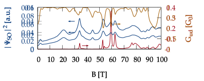
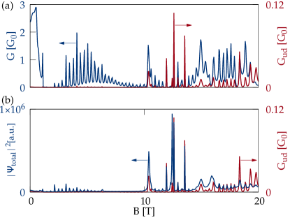
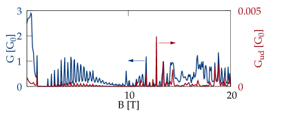
Formation of the current confinement at the n-p junction or resonances supported by adatoms presented above were due to the orbital effects of the external magnetic field that for the thin ribbon 292 atoms wide appeared only for the fields of the order of 50 T. In order to shift the magnetic field scale to lower values the wider ribbon is needed. The conductance for the fluorinated ribbon of width 125 nm is plotted in Fig. 14(a), still without the Zeeman interaction. The spin-flips occur already for of the order of 10 T and are correlated with formation of localized resonances within the fluorinated ribbon segment (Fig. 14(b)).
All the results presented above were obtained without the spin Zeeman effect. Figure 15 shows the conductance as a function of the external magnetic field with the Zeeman interaction. The peaks of appear but reduced by a factor of . Similarly, for the n-p junctions induced by external potential the spin-flipping contribution to conductance is drastically reduced by the spin Zeeman interaction. In presence of the spin Zeeman interaction for the perpendicular magnetic field the electron spin on its motion from one adatom to the other precesses with respect to the axis. This precession does not change the average value, only the perpendicular components and are affected. The spin precession length at 10 T is 1.785 µm, i.e. by orders of magnitude larger than the average distance between the F-F adatoms ( nm). The effect behind the reduction of the spin flipping conductance with the Zeeman interaction is the spin dependent Fermi wave vector. In the disordered sample the scattering wave function is very sensitive to the value of the Fermi wave vector and the accumulation of the spin precession events requires that the electron stays on its path while its spin is rotated. This is no longer the case when the spin Zeeman effect is present. The solution to this problem is given in the next subsection.
III.6 Side-attached quantum rings
A way to keep the electron on its path while the spin is rotated is the application of a lateral confinement of e.g. quantum ring as in Fig. 3. The quantum ring mre2 supports localized resonances with the current circulation of a fixed orientation. The results for the ring attached to the thin ribbon with the Zeeman interaction is given in Fig. 16. The spin-flipping contributions to conductance acquire values in spite of the presence of the spin Zeeman interaction.
The overall conductance is a symmetric function of the external magnetic field in consistence with the Onsager relation for a two-terminal device. Nevertheless, the spin-flipping contribution to conductance depends on the orientation of the magnetic field. The spin flips occur only for , i.e. for the magnetic field oriented in the direction which injects mre2 ; szmel the incident electron wave function from the ribbon to the quantum ring. The injection occurs only provided that a localized resonance is supported by the ring for the applied value of the magnetic field mre2 . For strong magnetic field oriented in the direction, the electron wave function is kept to the lower edge of the ribbon and does not notice the presence of the ring. This fact – with the Onsager relation – leads to limit for high magnetic fields inducing the quantum Hall conditions (see Fig. 16(a)).
IV Summary and conclusions
We studied charge and spin transport across a graphene nanoribbon with dilute fluorine adatoms using the wave function matching technique within the tight-binding approach. The electron passage below a single F adatom induces a small rotation of the electron spin due to the spin precession by a local Rashba interaction. In order to produce a spin-flip many the micro precession events at separate adatoms need to accumulate. We demonstrated that the necessary accumulation occurs when the electron circulates around a closed path in the external magnetic field in localized resonant states supported by an induced n-p junction or by the adatoms themselves. The spin-flipping effect is deteriorated by the spin Zeeman interaction which introduces the spin dependence to the electron trajectory. The dependence is of a secondary importance for a quantum ring side-attached to the nanoribbon which supports the localized resonances with a fixed electron circulation around the ring and allows for large spin-flipping contribution to conductance for the magnetic field orientation which injects the incident electron to the ring.
Acknowledgments
This work was supported by the National Sci- ence Centre (NCN) according to decision DEC- 2015/17/B/ST3/01161. The calculations were performed on PL-Grid Infrastructure
References
- (1) I. Zutic, J. Fabian, and S. Das Sarma, Rev. Mod. Phys. 76, 323 (2004).
- (2) S. Datta and B. Das, Appl. Phys. Lett. 56, 665 (1990).
- (3) A. H. Castro Neto, F. Guinea, N. M. R. Peres, K. S. Novoselov, and A. K. Geim, Rev. Mod. Phys. 81, 109 (2009).
- (4) W. Han and R. K. Kawakami, Phys. Rev. Lett. 107, 047207 (2011).
- (5) T. Maassen, J.J. van den Berg, N. Ijbema, F. Fromm, T. Seyller, R. Yakimova, and B.J. van Wees, Nano Lett., 12, 1498 (2012).
- (6) A. Manchon, H.C. Koo, J. Nitta, S.M. Frolov, R.A. Duine, Nature Materials 14, 871. (2015)
- (7) E.A. Laird, F. Kuemmeth, G. Steele, K. Grove-Rasmussen, J. Nygård, K. Flensberg, L.P. Kouwenhoven, Rev. Mod. Phys. 87, 703 (2015).
- (8) A. Avsar, J. Y. Tan, T. Taychatanapat, J. Balakrishnan, G.K.W. Koon, Y. Yeo, J. Lahiri, A. Carvalho, A. S. Rodin, E.C.T. O’Farrell, G. Eda, A. H. Castro Neto and B. Özyilmaz, Nature Comm. 5, 4875 (2014).
- (9) M. Gmitra, D. Kochan, P. Högl, and J. Fabian, Phys. Rev. B 93, 155104 (2016).
- (10) V. N. Kotov, B. Uchoa, V. M. Pereira, F. Guinea, and A. H. Castro-Neto, Rev. Mod. Phys. 84, 1067 (2012).
- (11) O. Leenaerts, B. Partoens, and F.M. Peeters, Phys. Rev. B 80, 24522 (2009).
- (12) J. J. Palacios, J. Fernández-Rossier, L. Brey. Phys. Rev. B 77, 195428, (2008).
- (13) P. Haase, S. Fuchs, T. Pruschke, H. Ochoa, and F. Guinea. Phys. Rev. B. 83, 241408 (2011).
- (14) N. A. Pike, D. Stroud. Phys. Rev. B 89, 115428 (2014).
- (15) F. Gargiulo, G. Autès, N. Virk, S. Barthel, M. Rosner, L.R.M. Toller, T.O. Wehling, and O. Yazyev. Phys. Rev. Lett. 113, 2476601 (2014).
- (16) J. Zhou, Q. Wang, Q. Sun, X.S. Chen, Y. Kawazoe and P. Jena. Nano Lett. 9, 3867, (2009).
- (17) M. Sepioni, R.R. Nair, S. Rablen, J. Narayanan, F. Tuna, R. Winpenny, A.K. Geim, and I. R. Grigorieva. Phys. Rev. Lett. 105, 207205 (2010).
- (18) X. Hong, S.-H. Cheng, C. Herding, and J. Zhu, Phys. Rev. B 83, 085410 (2011).
- (19) R. R. Nair, M. Sepioni, I.-L. Tsai, O. Lehtinen, J. Keinonen, A. V. Krasheninnikov, T. Thomson, A. K. Geim, and I. V. Grigorieva, Nat. Phys. 8, 199 (2012).
- (20) X. Hong, K. Zou, B. Wang, S.-H. Cheng, and J. Zhu, Phys. Rev. Lett. 108, 226602 (2012).
- (21) H. Santos and L. Henrard, J. Phys. Chem. C 118, 27074 (2014).
- (22) S. Irmer, T. Frank, S. Putz, M. Gmitra, D.Kochan, and J. Fabian, Phys. Rev. B 91, 115141 (2015).
- (23) R. R. Nair, M. Sepioni, I.-L. Tsai, O. Lehtinen, J. Adam A. Stabile, Aires Ferreira, Jing Li, N. M. R. Peres, and J. Zhu, Phys. Rev. B 92, 121411(R) (2015).
- (24) A. Sadeghi, M. Neek-Amal, G. R. Berdiyorov, and F. M. Peeters, Phys. Rev. B 91, 014304 (2015).
- (25) K. Wakabayashi, Y. Takane, M. Yamamoto, and M. Sigrist, Carbon 47, 124 (2009).
- (26) P. Chuang, S.-C. Ho, L. W. Smith, F. Sfigakis, M. Pepper, C.-H. Chen, J.-C. Fan, J. P. Griffiths, I. Farrer, H. E. Beere, G. A. C. Jones, D. A. Ritchie, and T.-M. Chen, Nature Nano. 10, 35 (2015).
- (27) D. A. Abanin and L. S. Levitov, Science 317, 641 (2007).
- (28) J. R. Williams, L. DiCarlo, and C. M. Marcus, Science 317, 638 (2007).
- (29) J. Tworzydło, I. Snyman, A. R. Akhmerov, and C. W. J. Beenakker, Phys. Rev. B 76, 035411 (2007).
- (30) J. R. Williams, T. Low, M. S. Lundstrom, and C. M. Marcus, Nat. Nanotechnol. 6, 222 (2011).
- (31) A. Cresti, G. Grosso, and G. P. Parravicini, Phys. Rev. B 77, 233402 (2008).
- (32) T. Taychatanapat, J. Y. Tan, Y. Yeo, K. Watanabe, T. Taniguchi, and B. Özyilmaz, Nat. Commun. 6, 6093 (2015).
- (33) P. Rickhaus, P. Makk, M.-H. Liu, E. Tóvári, M. Weiss, R. Maurand, K. Richter, and C. Schönenberger, Nat. Commun. 6, 6470 (2015).
- (34) K. Kolasiński, A. Mreńca-Kolasińska, and B. Szafran, Phys. Rev. B 95, 045304 (2017).
- (35) J. R. Williams and C. M. Marcus Phys. Rev. Lett. 107, 046602 (2011).
- (36) P. Carmier, C. Lewenkopf, and D. Ullmo, Phys. Rev. B 84, 195428 (2011).
- (37) M. Barbier, G. Papp, and F. M. Peeters, Appl. Phys. Lett. 100 , 163121 (2012); S. P. Milovanović, M. Ramezani Masir, and F. M. Peeters, Appl. Phys. Lett. 105, 123507 (2014).
- (38) N. Davies, A. A. Patel, A. Cortijo, V. Cheianov, F. Guinea, and V. I. Fal’ko, Phys. Rev. B 85, 155433 (2012).
- (39) J.-C. Chen, X. C. Xie, and Q.-F. Sun, Phys. Rev. B 86, 035429 (2012).
- (40) Y. Liu, R. P. Tiwari, M. Brada, C. Bruder, F. V. Kusmartsev, and E. J. Mele, Phys. Rev. B 92, 235438 (2015).
- (41) T. Taychatanapat, K. Watanabe, T. Taniguchi, and P. Jarillo-Herrero, Nat. Phys. 9, 225 (2013).
- (42) S. Bhandari, G.-H. Lee, A. Klales, K. Watanabe, T. Taniguchi, E. Heller, P. Kim, and R. M. Westervelt, Nano Lett. 16, 1690 (2016).
- (43) M.-H. Liu, C. Gorini, and Klaus Richter, Phys. Rev. Lett. 118, 066801 (2017).
- (44) A. Mreńca-Kolasińska, S. Heun, and B. Szafran Phys. Rev. B 93, 125411 (2016).
- (45) A. Mreńca-Kolasińska and B. Szafran, Phys. Rev. B 94, 195315 (2016).
- (46) F. V. Tikhonenko, D. W. Horsell, R. V. Gorbachev, and A. K. Savchenko Phys. Rev. Lett. 100, 056802 (2008).
- (47) D. Cabosart, S. Faniel, F. Martins, B. Brun, A. Felten, V. Bayot, and B. Hackens, Phys. Rev. B 90, 205433 (2014).
- (48) S. Russo, J. B. Oostinga, D. Wehenkel, H. B. Heersche, S. S. Sobhani, L. M. K. Vandersypen, and A. F. Morpurgo, Phys. Rev. B 77, 085413 (2008).
- (49) D. Smirnov, J. C. Rode, and R. J. Haug, Appl. Phys. Lett. 105, 082112 (2014).
- (50) M. Huefner, F. Molitor, A. Jacobsen, A. Pioda, C. Stampfer, K. Ensslin, and T. Ihn, New J. Phys. 12, 043054 (2010).
- (51) J. Dauber, M. Oellers, F. Venn, A. Epping, K. Watanabe, T. Taniguchi, F. Hassler, and C. Stampfer, Phys. Rev. B 96, 205407.
- (52) M. Y. Han, B. Ozyilmaz, Y. B. Zhang, P. Kim, Phys. Rev. ¨ Lett. 98, 206805 (2007).
- (53) Z. H. Chen, Y. M. Lin, M. J. Rooks, P. Avouris, Physica E 40, 228 (2007).
- (54) M. Evaldsson, I. V. Zozoulenko, H. Xu, and T. Heinzel, Phys. Rev. B 78, 161407(R) (2008).
- (55) T.O. Wehling, M.I. Katsnelson, and A. I. Lichtenstein, Phys. Rev. B 80, 085428 (2009).
- (56) R. M. Guzmán-Arellano, A. D. Hernández-Nieves, C. A. Balseiro, and Gonzalo Usaj, Appl. Phys. Lett. 105, 121606 (2014).
- (57) C.L. Kane and E.J. Mele, Phys. Rev. Lett. 95, 226801 (2005).
- (58) C.-C. Liu, Hua Jiang, and Yugui Yao, Phys. Rev. B 84, 195430 (2011).
- (59) K. Kolasiński and B. Szafran Physical Review B 88, 165306 (2013).
- (60) M. Zwierzycki, P. A. Khomyakov, A. A. Starikov, K. Xia, M. Talanana, P. X. Xu, V. M. Karpan, I. Marushchenko, I. Turek, G. E. W. Bauer, G. Brocks, and P. J. Kelly, phys. stat. sol. (b) 245, 623 (2008).
- (61) C. Pacher, C. Rauch, G. Strasser, E. Gornik, F. Elsholz, A. Wacker, G. Kiesslich, and E. Schöll, Appl. Phys. Lett. 79, 1486 (2001).
- (62) S. Ihnatsenka and G. Kirczenow Phys. Rev. B 85, 121407(R) (2012).
- (63) N. Tombros, A. Veligura, J. Junesch, M.H.D. Guimaraes, I.J. Vera-Marun, H. T. Jonkman, and B. J. van Wees, Nat. Phys. 7, 697 (2011).
- (64) L. Meier, G. Salis, I. Shorubalko, E. Gini, S. Schön, and Klaus Ensslin, Nat. Phys. 3, 650 (2007).
- (65) S. Bednarek and B. Szafran, Phys. Rev. Lett. 101, 216805 (2008).