Development of a very low-noise cryogenic pre-amplifier for large-area SiPM devices
Abstract
Silicon Photomultipliers (SiPMs) are an excellent candidate for the development of large-area light sensors. Large SiPM-based detectors require low-noise pre-amplifiers to maximize the signal coupling between the sensor and the readout electronics. This article reports on the development of a low-noise transimpedance amplifier sensitive to single-photon signals at cryogenic temperature. The amplifier is used to readout a 1 cm2 SiPM with a signal to noise ratio in excess of 40.
Index Terms:
SiPMs, SiGe, cryogenic electronics, low noise amplifier, transimpedance amplifier.I Introduction
The improvements in performance of SiPMs at cryogenic temperature [1] and the availability of low-noise hetero-junction amplifiers open the door to the development of cryogenic, large-area, SiPM-based photo-detectors as replacements for photomultiplier tubes. We introduce and describe a low-noise transimpedance amplifier designed to instrument large-area assemblies of SiPMs intended for operation at cryogenic temperature. As the scale and sensitivity of rare-event physics searches grows, so does the need for large, high efficiency light detectors. These amplifiers were designed for use in the DarkSide-20k dark matter detector, which will instrument an active volume of about of liquid argon with of SiPMs [2]. Due to their excellent signal to noise performance, they are also generally useful as the building block for realization of other large SiPM assemblies.
Development of the amplifier was done in a dedicated cryogenic setup, consisting of a Cryomech PT90 pulse tube cryocooler mounted on the top flange of a stainless steel cryostat evacuated to . The cryocooler cold finger extends into the cryostat and holds the devices under test. The temperature of the cold finger is monitored by a set of platinum RTDs and regulated by a Lakeshore 335 to within of a set-point temperature. The setup is capable of operating within the range from .
The core of the transimpedance amplifier is a LMH6629 high-speed operational amplifier from Texas Instruments. The cryogenic characterization of the LMH6629 will be described in Section II. The characteristics of the SiPMs used for testing, the design of the transimpedance amplifier and the analysis algorithms will be discussed in Section III. Finally, the results of the read-out of a SiPM will be described in Section IV.
II LMH6629 Characterization
The performance of standard Silicon Bipolar Junction Transistors (BJT) degrades at cryogenic temperatures [3] whereas that of Hetero-junction Bipolar Transistors (HBT) does not, making HBTs an interesting alternative to CMOS technology for cryogenic applications. An HBT is a type of bipolar junction transistor that uses different semiconductor materials for the emitter and base regions. Among the available technologies, Silicon Germanium (SiGe) HBTs, which are manufactured by many foundries for high bandwidth applications, are particularly well-suited for cryogenic operation because of their bandgap-engineered base [4].
The LMH6629 is a high speed, ultra-low noise amplifier fabricated with SiGe technology by Texas Instruments. The device is designed for applications requiring a wide bandwidth with high gain and low noise [5]. The amplifier is available in two packages, a standard SOT-23-5 and a lead-less WSON-8. The WSON-8 package has selectable internal compensation for operation at low gains. Without this additional compensation enabled, the amplifier is stable only for gains larger than at cryogenic temperatures. This work focuses on the WSON-8 package, which was selected because its die attach pad improves thermalization.
Measurements of the LMH6629 were performed on custom FR4 printed circuit boards installed on the cold finger of the cryogenic setup. The passive components in the circuit were carefully selected for their cryogenic compatibility. All of the capacitors in the circuit are either C0G/NP0 or PPS [6], and the resistors are based on thin or thick metal film.
II-A Bandwidth
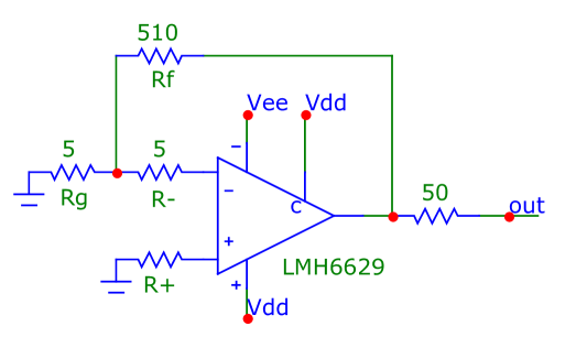
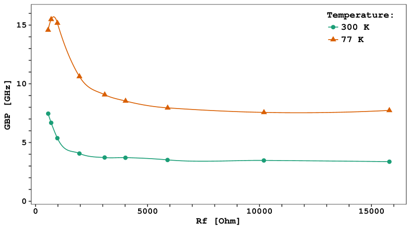
The measurement of the intrinsic bandwidth of the LMH6629 is complicated by parasitic effects from the circuit in which the chip is operated. In fact, a small capacitance on the feedback path can significantly reduce the measured bandwidth. Such behavior is demonstrated in Figure 2, where the Gain Bandwidth Product (GBP) of the test circuit is shown for different feedback resistor () values. The GPB rapidly decreases as increases, eventually reaching a plateau. The spice simulation described in Section II-F models this effect by including a feedback parasitic capacitance ().
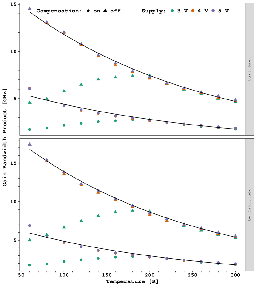
The GBP was measured by extracting the noise gain and the frequency of the half-power point () from spectra collected with an Agilent model 5071c Vector Network Analyzer (VNA) configured for S21 scans. Figure 3 shows the GBP temperature dependence measured in both the inverting and non-inverting configurations (). The GBP of the amplifier is exponential with temperature as shown by the fit in Figure 3. When operated with a power supply, the amplifier performance quickly degrades below .
II-B Input bias current
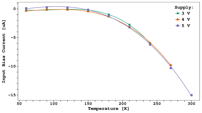
The input bias current () of the LMH6629 was determined using the circuit shown in Figure 2 with . The DC output of the circuit is given by , with . The results of the measurement are shown in Figure 5. At room temperature, , in agreement with the value reported on the datasheet. It is interesting to note that the input bias current rapidly decreases at low temperature, reaching a plateau of about at about .
II-C Input noise
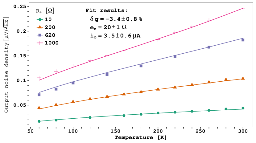
Measurements of the voltage () and current () noise terms as a function of temperature were done with the LMH6629 configured as shown in Figure 2. The amplifier output was acquired with an R&S FSV 7 spectrum analyzer and an R&S RTO1024 oscilloscope operating as a spectrum analyzer. The output noise density was determined at in a flat region of the power spectra, far from any environmental noise pickup and the half-power point. Figure 5 shows the results for several values of along with fits to the noise model described below.
The output noise density () as a function of temperature () can be expressed as
| (1) |
where is the Boltzmann constant,
Equation 1 accounts for the Johnson-Nyquist noise of the resistors in the circuit and for the intrinsic noise sources of the LMH6629.
The fit model assumes that behaves like a Johnson-Nyquist noise source with resistance () and that is due to the shot noise of the input current ( with the input bias current, , measured in Section II-B and assumed constant). The best fit values are:
-
•
, which at is equivalent to , compared to on the datasheet;
-
•
, for a total shot noise density of , compared to on the datasheet;
-
•
and , where is the relative variation of the gain with respect to the theoretical value and is allowed to float during the fit.
Overall, the experimental values are well described by the model. The standard deviation of the relative residuals is , mostly due to the measurements performed with large values. This indicates that the accuracy of the scaling model of the current noise with temperature needs to be improved. However, in this work has no effect on the overall noise budget given the small value of the resistors in use (see Section III-C).
II-D Dynamic range
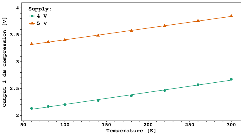
The dynamic range of the LMH6629 output was measured using the VNA configured for a power sweep at in S21 mode. Figure 7 shows the compression point as a function of temperature for two different power supply voltages ( and ) along with a linear fit to the data. Figure 7 plots the peak to peak voltage. When the circuit is used as a pulse amplifier, the effective dynamic range is halved.
II-E Power consumption
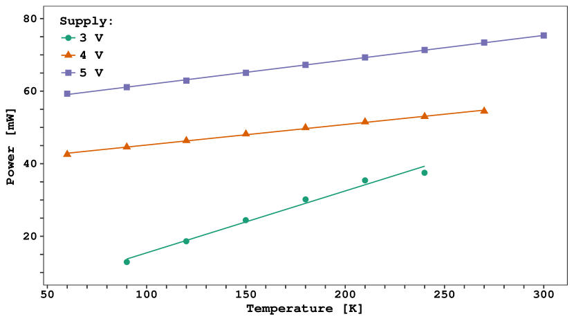
The power consumption of the LMH6629 was estimated by measuring the current flowing in the circuit when no load was connected to the output. Figure 7 shows the results for various supply voltages along with a linear fit to the data.
II-F Simulation
Texas Instruments provides a SPICE model of the LMH6629 that was verified with Microcap 10 from Spectrum Software. While the noise simulation is accurate at better than a few percent within the temperature range of interest, the simulated bandwidth does not follow the experimental behavior of the amplifier, consistently predicting a smaller GBP than what was measured (up to a factor of more than 2) for temperatures below .
III Transimpedance Amplifier
Based on the performance of the LMH6629, a low-noise transimpedance amplifier was designed for cryogenic applications.
| Frequency | ||||
|---|---|---|---|---|
| [] | [] | [] | [] | |
III-A NUV-HD-LF SiPM
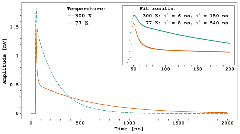
The transimpedance amplifier was optimized for use with a custom batch of NUV-HD-LF area SiPMs produced by FBK for DarkSide-20k [2]. These devices are similar to FBK’s standard NUV-HD technology [7] but are engineered to have a lower field strength in the avalanche region [8] and a smaller quenching resistance ( at room temperature) to provide a relatively fast signal. The average photoelectron signal from a NUV-HD-LF SiPM is shown in Figure 8, both at room and liquid nitrogen temperature. These SiPMs can be operated in liquid nitrogen with gains up to . In this work, the SiPM operating voltage is tuned so that at each operating temperature, the gain remains stable at .
The recharge time constant of the SiPM was determined over the interval by a fit to the formula
| (2) |
where and with a standard deviation of the relative residuals of .
In addition to the characteristics of the NUV-HD-LF SiPMs reported in [1], the detector equivalent capacitance () and its equivalent series resistance () are relevant for this work. As discussed in [9], these parameters are the result of the summing of all the microcell properties: resistance of the quenching resistor (), capacitance of the quenching resistor () and the cell intrinsic capacitance (). The characterization of the microcell properties at cryogenic temperatures is beyond the scope of this paper. A direct measurement of and was done using an Agilent E4980A RLC meter and the results are reported in Table I.
Some observations can be made from the measurement of and . First, while the detector capacitance remains relatively constant with temperature variation, increases in liquid nitrogen by about a factor of five. This is due to the large variation of , which is a poly-silicon resistor. This in turn increases the SiPM recharge time. Second, both and vary as a function of frequency. To first order, , , and form a filter network with one pole in , which at room temperature has a value in the range (see [9]). For higher frequencies, asymptotically approaches zero. At cryogenic temperature, the larger value of shifts the pole down to a few MHz. By assuming a ratio /, can be estimated as corresponding to at room temperature and at .
III-B Pre-amplifier design
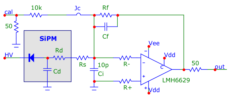
The schematic of the transimpedance amplifier is shown in Figure 9. The circuit is based on an LMH6629 operating with a supply voltage and its on-chip compensation reduced.
The resistors and (both ) at the inverting and non-inverting inputs are required to avoid high frequency oscillations at cryogenic temperature. This is done at the cost of a roughly increase in the voltage noise, . The capacitor minimizes undershoot due to the fast discharge of the SiPM. The feedback capacitance, , is only a few hundred and is due to the stray capacitance of the printed circuit board, as discussed in Section II-A.
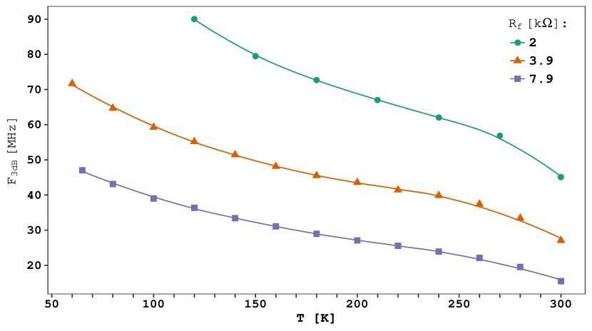
The series resistor, (and to some extent ), plays an important role in the performance of the amplifier. For frequencies above , the system behaves like an inverting amplifier due to the presence of and . This means that the bandwidth is proportional to the GBP of the amplifier, in contrast to an ideal TIA, where the bandwidth scales as the square root of the GBP. The result is an increased bandwidth. Figure 10 shows the temperature scaling of the pre-amplifier bandwidth as measured by VNA scans between the calibration input and the output with the SiPM connected. In addition, the series resistor changes the noise gain so that, for frequencies above , it plateaus at . This in turn reduces the output noise without changing the transfer function for current sources (like SiPMs).
However, large values of will alter the output signal shape by creating a low-pass filter with the detector capacitance and, more importantly, significantly contribute to the noise budget.
III-C Pre-amplifier performance in liquid nitrogen
Values of and were selected to optimize the TIA performance at . With these values, the bandwidth of the pre-amplifier is always significantly higher than the fast rising edge of the SiPM (which is between and is extracted from the fit of the fast component of the waveform shown in Figure 8).
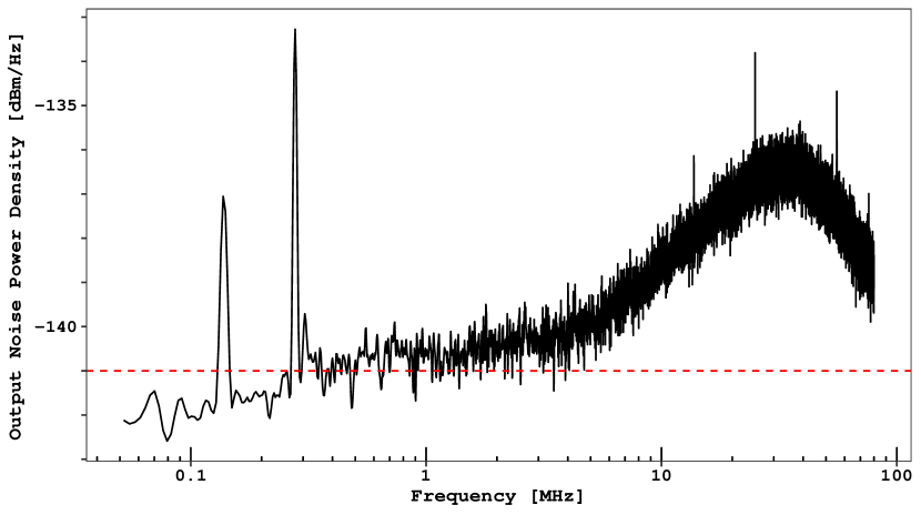
Above , the voltage noise at the input of the amplifier, , includes the intrinsic voltage noise of the LMH6629, , and the Johnson-Nyquist noise of the other resistors in the circuit. In this formula, accounts for , as described in Section II-C. In liquid nitrogen corresponding to about at the output (taking into account the back termination of the output). The input current noise of the LMH6629, , and the Johnson-Nyquist current noise of together account for about , which corresponds to about at the output and can therefore be ignored. Figure 11 shows the output noise density spectrum of the pre-amplifier connected to the NUV-HD-LF SiPM. The difference at between the prediction and the measurement is less than .
The high frequency bump present in the noise spectrum is due to the decrease of at few MHz as described at the end of Section III-A. With a vanishing , the noise gain increases up to a theoretical factor of . In practice this value is never reached due to the limited available GBP.
With a power supply, the pre-amplifier provides a dynamic range in excess of photo-electrons with a power consumption of about .
III-D Readout and Data analysis
Cryogenic tests of the transimpedance amplifier with the NUV-HD-LF SiPM were performed in the setup described in Section I. A Hamamatsu PLP-10 laser, capable of sub-nanosecond light pulses, was used as a light source. The signal from the transimpedance amplifier was fed out of the cryostat into a room temperature, low-noise amplifier and then digitized by a 10 bit, 2 GS/s CAEN V1751 configured with a pre-trigger of and a total gate length of . The digitizer was triggered by the sync pulse of the PLP-10. The least significant bit of the digitizer is so further amplification of the signal is required to avoid excessive quantization noise. A custom low noise amplifier based on two THS3201 operational amplifiers [10] was built providing a bandwidth in excess of , a gain of , and an input noise density of about .
Offline analysis software was used to analyze the digitized waveforms and calculate the figures of merit. Of particular interest is the signal to noise ratio (SNR), defined as the ratio between the gain of the photoelectron peaks and the baseline noise. Two SNR parameters were calculated based on two different methods for calculating the charge of each waveform: the amplitude of the raw waveform at the peak () and the amplitude of the digitally filtered waveform at the peak (). In both cases, the baseline noise was estimated as the standard deviation of the corresponding pre-trigger raw or filtered waveform.
III-E Matched filter
The extraction of a signal with known shape from stochastic noise is maximized by the use of a matched filter [11]. Matched filtering is done by convolving the raw waveform with a time reversed template waveform. The matched filter algorithm is implemented offline. For a given pre-amplifier configuration and temperature, the the template waveform is determined by averaging baseline subtracted and time aligned waveforms from single photoelectron events. The filtered waveform exhibits a symmetric shape around the photo-electron arrival time, where a peak is present. The identification of the charge and timing of the signal is performed by evaluating the amplitude and the timing of the filtered waveform maximum.
IV Results
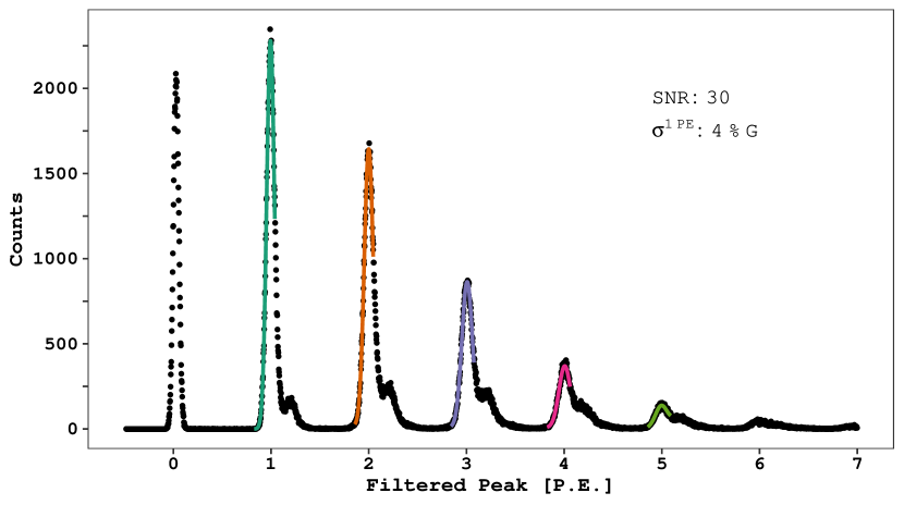
The spectrum obtained using a NUV-HD-LF SiPM at and the matched filter algorithm described in Section III-E is shown in Figure 12. An SNR of is achieved with the SiPM operating at a gain of .
IV-A Signal over noise
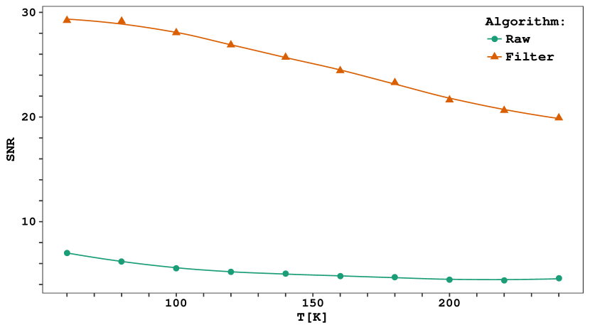
Figure 13 compares and as a function of temperature. The behavior of these curves includes many effects. To first order, both the signal amplitude and the baseline noise increase with higher temperature. A simple model that only considers the temperature dependence of the amplitude and the noise plateau over-predicts the decrease in SNR at room temperature. This is because the magnitude and shape of the output noise spectrum changes due to the temperature dependence of the TIA bandwidth, , and . The net effect on the baseline noise at the bandwidth of interest, which is also temperature dependent, is therefore difficult to model analytically.
IV-B Timing
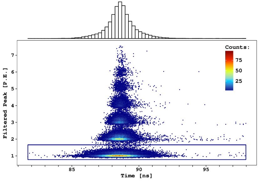
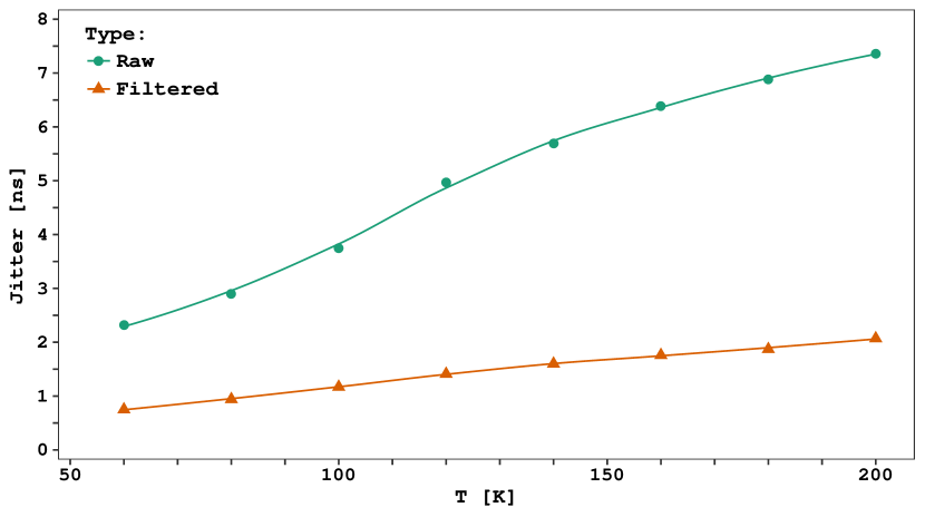
The rise-time of the unfiltered SiPM signal is a function of the amplifier bandwidth shown in Figure 10 and is between 5 and 11 ns (modeling the rise-time as 0.35/bandwidth). Given the relatively low , a standard discriminator is not the best approach for determining the event timing. In situations like this, it is advantageous to use the entire SiPM waveform for event reconstruction. This is particularly true at cryogenic temperature, when a large fraction of the total signal charge is contained in the slow recharge of the waveform. This is done using matched filtering, which preserves the fast component of the signal while maximizing the SNR and yielding nanosecond timing resolution. Figure 14 shows the time jitter of the reconstructed event time relative to the laser pulse measured using the matched filtered waveform at . The standard deviation of the first photoelectron peak is .
Figure 15 shows the time distribution as a function of temperature for both filtered and unfiltered waveforms (in this case using a simple threshold to define the timing). While the timing resolution of the filtered waveform is slightly affected by the temperature, the performance of the unfiltered waveform shows a strong degradation with temperature. This is expected because the jitter of a simple discrimination can be quantified as the quotient of the risetime divided by the signal to noise ratio. In our setup the SNR decreases with temperature (Figure 13) and the bandwidth decreases with temperature (Figure 10), significantly reducing the fast rising edge of the waveform.
V Conclusions
SiPM-based, cryogenic photo-detectors with large active areas have great appeal for use in low-background particle physics experiments, where improvements in photo-detection efficiency, resolution, and radio-purity directly impact experimental reach. The viability of such photo-detectors relies on the development of cryogenic pre-amplifiers capable of preserving the fidelity of photon signals despite large sensor capacitance. In this paper, measurements of the electrical characteristics of a Texas Instruments LMH6629 were made over a range of temperatures from room temperature to and a cryogenic transimpedance amplifier was designed around the device. The resulting amplifier design was operated with a NUV-HD-LF SiPM with an SNR of at when operating the SiPM at a gain of ( of overvoltage) and timing resolution better than , thus demonstrating the practicality of large-area SiPM detectors as conventional photomultiplier tube replacements for cryogenic applications.
References
- [1] F. Acerbi, S. Davini, A. Ferri, C. Galbiati, G. Giovanetti, A. Gola, G. Korga, A. Mandarano, M. Marcante, G. Paternoster, C. Piemonte, A. Razeto, V. Regazzoni, D. Sablone, C. Savarese, G. Zappala, and N. Zorzi, “Cryogenic Characterization of FBK HD Near-UV Sensitive SiPMs,” IEEE Trans. Elec. Dev., pp. 1–6, 2017. [Online]. Available: http://ieeexplore.ieee.org/document/7807295/
- [2] C. E. Aalseth, F. Acerbi, P. Agnes, I. F. M. Albuquerque, T. Alexander, A. Alici, A. K. Alton, P. Antonioli, S. Arcelli, R. Ardito, I. J. Arnquist, D. M. Asner, M. Ave, H. O. Back, A. I. B. Olmedo, G. Batignani, E. Bertoldo, S. Bettarini, M. G. Bisogni, V. Bocci, A. Bondar, G. Bonfini, W. Bonivento, M. Bossa, B. Bottino, M. G. Boulay, R. Bunker, S. Bussino, A. F. Buzulutskov, M. Cadeddu, M. Cadoni, A. Caminata, N. Canci, A. Candela, C. Cantini, M. Caravati, M. Cariello, M. Carlini, M. Carpinelli, A. Castellani, S. Catalanotti, V. Cataudella, P. Cavalcante, S. Cavuoti, R. Cereseto, A. Chepurnov, C. Cicalò, L. Cifarelli, M. Citterio, A. G. Cocco, M. Colocci, S. Corgiolu, G. Covone, P. Crivelli, I. D’Antone, M. D’Incecco, D. D’Urso, M. D. Da Rocha Rolo, M. Daniel, S. Davini, A. De Candia, S. De Cecco, M. De Deo, G. De Filippis, G. De Guido, G. De Rosa, G. Dellacasa, M. Della Valle, P. Demontis, A. Derbin, A. Devoto, F. Di Eusanio, G. Di Pietro, C. Dionisi, A. Dolgov, I. Dormia, S. Dussoni, A. Empl, M. F. Diaz, A. Ferri, C. Filip, G. Fiorillo, K. Fomenko, D. Franco, G. E. Froudakis, F. Gabriele, A. Gabrieli, C. Galbiati, P. G. Abia, A. Gendotti, A. Ghisi, S. Giagu, P. Giampa, G. Gibertoni, C. Giganti, M. A. Giorgi, G. K. Giovanetti, M. L. Gligan, A. Gola, O. Gorchakov, A. M. Goretti, F. Granato, M. Grassi, J. W. Grate, G. Y. Grigoriev, M. Gromov, M. Guan, M. B. B. Guerra, M. Guerzoni, M. Gulino, R. K. Haaland, A. Hallin, B. Harrop, E. W. Hoppe, S. Horikawa, B. Hosseini, D. Hughes, P. Humble, E. V. Hungerford, A. M. Ianni, C. Jillings, T. N. Johnson, K. Keeter, C. L. Kendziora, S. Kim, G. Koh, D. Korablev, G. Korga, A. Kubankin, M. Kuss, B. Lehnert, X. Li, M. Lissia, G. U. Lodi, B. Loer, G. Longo, P. Loverre, R. Lussana, L. Luzzi, Y. Ma, A. A. Machado, I. N. Machulin, A. Mandarano, L. Mapelli, M. Marcante, A. Margotti, S. M. Mari, M. Mariani, J. Maricic, C. J. Martoff, M. Mascia, M. Mayer, A. B. McDonald, A. Messina, P. D. Meyers, R. Milincic, A. Moggi, S. Moioli, J. Monroe, A. Monte, M. Morrocchi, B. J. Mount, W. Mu, V. N. Muratova, S. Murphy, P. Musico, R. Nania, A. N. Agasson, I. Nikulin, V. Nosov, A. O. Nozdrina, N. N. Nurakhov, A. Oleinik, V. Oleynikov, M. Orsini, F. Ortica, L. Pagani, M. Pallavicini, S. Palmas, L. Pandola, E. Pantic, E. Paoloni, G. Paternoster, V. Pavletcov, F. Pazzona, S. Peeters, K. Pelczar, L. A. Pellegrini, N. Pelliccia, F. Perotti, R. Perruzza, V. P. Fortes, C. Piemonte, F. Pilo, A. Pocar, T. Pollmann, D. Portaluppi, D. A. Pugachev, H. Qian, B. Radics, F. Raffaelli, F. Ragusa, M. Razeti, A. Razeto, V. Regazzoni, C. Regenfus, B. Reinhold, A. L. Renshaw, M. Rescigno, F. Retiere, Q. Riffard, A. Rivetti, S. Rizzardini, A. Romani, L. Romero, B. Rossi, N. Rossi, A. Rubbia, D. Sablone, P. Salatino, O. Samoylov, E. S. García, W. Sands, M. Sant, R. Santorelli, C. Savarese, E. Scapparone, B. Schlitzer, G. Scioli, E. Segreto, A. Seifert, D. A. Semenov, A. Shchagin, L. Shekhtman, E. Shemyakina, A. Sheshukov, M. Simeone, P. N. Singh, P. Skensved, M. D. Skorokhvatov, O. Smirnov, G. Sobrero, A. Sokolov, A. Sotnikov, F. Speziale, R. Stainforth, C. Stanford, G. B. Suffritti, Y. Suvorov, R. Tartaglia, G. Testera, A. Tonazzo, A. Tosi, P. Trinchese, E. V. Unzhakov, A. Vacca, E. Vázquez-Jáuregui, M. Verducci, T. Viant, F. Villa, A. Vishneva, R. B. Vogelaar, M. Wada, J. Wahl, J. Walding, S. E. Walker, H. Wang, Y. Wang, A. W. Watson, S. Westerdale, R. Williams, M. M. Wojcik, S. Wu, X. Xiang, X. Xiao, C. Yang, Z. Ye, A. Y. de Llano, F. Zappa, G. Zappalà, C. Zhu, A. Zichichi, M. Zullo, and A. Zullo, “DarkSide-20: A 20 Tonne Two-Phase LAr TPC for Direct Dark Matter Detection at LNGS,” arXiv, 2017. [Online]. Available: http://arxiv.org/abs/1707.08145v1
- [3] W. P. Dumke, “The effect of base doping on the performance of Si bipolar transistors at low temperatures,” IEEE Trans. Elec. Dev., vol. 28, no. 5, pp. 494–500, 1981. [Online]. Available: http://ieeexplore.ieee.org/document/1481524/
- [4] J. D. Cressler, “Operation of SiGe bipolar technology at cryogenic temperatures,” J. Phys. IV France, vol. 04, no. C6, pp. C6–101–C6–110, 1994. [Online]. Available: http://www.edpsciences.org/10.1051/jp4:1994616
- [5] Texas Instruments, “LMH6629 Ultra-Low Noise, High-Speed Operational Amplifier with Shutdown,” Texas Instruments, Tech. Rep., 2016. [Online]. Available: www.ti.com/lit/ds/symlink/lmh6629.pdf
- [6] F. Teyssandier and D. Prêle, “Commercially Available Capacitors at Cryogenic Temperatures,” in WOLTE9, 2010. [Online]. Available: https://hal.archives-ouvertes.fr/hal-00623399
- [7] C. Piemonte, F. Acerbi, A. Ferri, A. Gola, G. Paternoster, V. Regazzoni, G. Zappala, and N. Zorzi, “Performance of NUV-HD Silicon Photomultiplier Technology,” IEEE Trans. Elec. Dev., vol. 63, no. 3, pp. 1111–1116, 2016. [Online]. Available: http://ieeexplore.ieee.org/lpdocs/epic03/wrapper.htm?arnumber=7397984
- [8] A. Ferri, F. Acerbi, A. Gola, G. Paternoster, C. Piemonte, and N. Zorzi, “Performance of FBK low-afterpulse NUV silicon photomultipliers for PET application,” JINST, vol. 11, no. 03, pp. P03 023–P03 023, 2016. [Online]. Available: http://stacks.iop.org/1748-0221/11/i=03/a=P03023?key=crossref.3b90668de68c0dbe8d723d4154a2ece8
- [9] D. Marano, M. Belluso, G. Bonanno, S. Billotta, A. Grillo, S. Garozzo, G. Romeo, O. Catalano, G. L. Rosa, G. Sottile, D. Impiombato, and S. Giarrusso, “Silicon photomultipliers electrical model extensive analytical analysis,” IEEE Transactions on Nuclear Science, vol. 61, no. 1, pp. 23–34, Feb 2014. [Online]. Available: http://ieeexplore.ieee.org/document/6661445/
- [10] Texas Instruments, “1.8-GHz, Low Distortion, Current-Feedback Amplifier,” Texas Instruments, Tech. Rep., 2003. [Online]. Available: http://www.ti.com/lit/ds/slos416c/slos416c.pdf
- [11] G. Turin, “An introduction to matched filters,” IEEE Trans. Inform. Theory, vol. 6, no. 3, pp. 311–329, 1960. [Online]. Available: http://ieeexplore.ieee.org/document/1057571/