Thermoelectric transport parallel to the planes in a multilayered Mott-Hubbard heterostructure
Abstract
We present a theory for charge and heat transport parallel to the interfaces of a multilayer (ML) of the ABA type, where A and B are materials with strongly correlated electrons. When separated, both materials are half-filled Mott-Hubbard insulators with large gaps in their excitation spectrum. In a ML, the renormalization of the energy bands gives rise to a charge reconstruction which breaks the charge neutrality of the planes next to the interface. The ensuing electrical field couples self-consistently to the itinerant electrons, so that the properties of the ML crucially depend on an interplay between the on-site Coulomb forces and the long range electrostatic forces. Using the Falicov-Kimball model, we compute the Green’s function and the local charge on each plane of the ML by inhomogeneous DMFT and find the corresponding electrical potential from Poisson’s equation. The self-consistent solution is obtained by an iterative procedure, which yields the reconstructed charge profile, the electrical potential, the planar density of states, the transport function, and the transport coefficients of the device. For the right choice of parameters, we find that a heterostructure built of two Mott-Hubbard insulators exhibits, in a large temperature interval, a linear conductivity and a large temperature-independent thermopower. The charge and energy currents are confined to the central part of the ML. Our results indicate that correlated multilayers have the potential for applications; by tuning the band shift and the Coulomb correlation on the central planes, we can bring the chemical potential in the immediate proximity of the Mott-Hubbard gap edge and optimize the transport properties of the device. In such a heterostructure, a small gate voltage can easily induce a MI transition. Furthermore, the right combination of strongly correlated materials with small ZT can produce, theoretically at least, a heterostructure with a large ZT.
pacs:
71.10.Fd, 71.27.+a, 71.30+h,72.15.Jf, 72.20-iI Introduction
Heterogeneous materials in which a large difference of the chemical potentials gives rise to the emergence of metallic sheets at the interfaces have recently attracted a great deal of attentionmillis_okamoto . The heterogeneous materials which are insulating but close to the metal-insulator (MI) transition might be of considerable technological interest but have not yet been theoretically studied. In this paper, we provide a description of the charge and energy transport in a multilayer (ML) consisting of three stacks of insulating planes. Two identical ones (material A) make up the left and the right semi-infinite leads, which are connected to the central section, composed of a different finite stack of insulating planes (material B). The leftmost and the rightmost plane of the self-consistently determined ML are attached to semi-infinite bulk materials which set the overall chemical potential of the device. When disconnected, materials A and B are half-filled Mott insulators with their chemical potentials located in the middle of their respective Mott-Hubbard gaps. In the ML, the properties change dramatically and, for the right choice of parameters, non-vanishing charge and heat currents emerge parallel to the interface.
The unusual properties of such multilayers result from the competition between the short-range Coulomb repulsion and long-range electrostatic energy, caused by the electronic charge redistribution. To study the ML, we use the spinless Falicov-Kimball model with large electron-electron interactionfalicov_kimball_1969 and compute the Green’s functions and the renormalized charge distribution with inhomogeneous dynamical mean-field theory (DMFT). The generalization to include spin is straightforward. The charge redistribution due to the interfaces, gives rise to a long range electrostatic potential that couples to electrons on each plane and affects their dynamics. The self-consistency of the solution is ensured by treating the DMFT equations for the Green’s functions and the charge density together with Poisson’s equation for the electrical potential.
The isolated subsystems A and B have an excitation spectrum that is symmetric around their respective chemical potentials but the bands in material B are shifted with respect to those in A by an energy . In the ML with a common chemical potential, the local density of states (DOS) on the planes in the leads is nearly the same as in the bulk, with the exception of the planes near the interface. On these planes there is an accumulation of charge and, consequently, the local DOS deviates from the bulk shape. In the central part, the local charge on most planes is also the same as in the bulk but the symmetry of excitations with respect to the common chemical potential is lost: the local DOS is shifted almost rigidly by , bringing one of the Hubbard band edges closer to the chemical potential. The charge on a few planes next to the interface is reduced and a local DOS on these planes is not just shifted but also distorted. Thus, the interfacing gives rise to a screened-dipole layer which greatly reduces the gap in the transport DOS and transforms the ML into a small-gap semiconductor with the chemical potential in the proximity of the band edge. An electric field applied perpendicularly to the planes can switch the device between semiconducting and metallic states. This switching does not involve the diffusion of electrons over macroscopic distances, so that the characteristic time-scale can be much shorter than in usual semiconductor devices.
The transport properties of the ML are obtained by linear response theory and the thermoelectric response of the ML is calculated by considering the electronic degrees of freedom only. Of course, in a ML with semi-infinite leads, the phonon conductivity parallel to the planes might not be small far enough from the interface. But since the main effect of the mismatch of the chemical potentials due to is the shift of the B-bands with respect to the A-bands, we expect similar features in a device with finite leads or in an ABAABAABA heterostructure.
The paper is organized as follows. In Sec.II, we introduce the model Hamiltonian of an inhomogeneous multilayer.
In Sec. III, we show how to obtain the planar Green’s functions by inhomogeneous DMFT and find the self-consistent solution
that satisfies Poisson’s equation. In that section, we also compute the stationary currents by linear response theory, find the transport function,
and obtain the transport integrals by the Jonson-Mahan theorem.
In Sec. IV, we present the numerical results for the charge redistribution, the renormalization of the electrical potential,
the single-particle spectral function, and show that the gap in the excitation spectrum is much reduced by interfacing.
We also discuss the results for the transport coefficients and the figure of merit of the device. Sec.V provides the conclusions and summary.
II The model Hamiltonian of a correlated multilayer
We perform self-consistent calculations for a ML of the ABA type with planes perpendicular to the -axis. There are identical planes (material A) in the left and right part, and planes (material B) in the central part, with assumed to be odd. The correlation effects are described by the spinless Falicov-Kimball model with the bulk concentration of 1/2 conduction and 1/2 localized electrons per site, and with a large on-site Coulomb repulsion between them. The electronic charge on each site is compensated by the background charge of the ionic cores which ensures charge neutrality. In the ML, the translational symmetry is preserved in the and directions but it is broken in the direction.
The leftmost self-consistent plane of the ML is labeled by index and the rightmost one by . These planes are connected to bulk reservoirs which set the overall chemical potential of the ML. The plane next to the interface in the left lead, the plane next to the interface in the central part, and the mirror symmetry plane of the ML, are indexed by , , and , respectively (with the symmetry mirror in the center of the device). In what follows, the planes are denoted by Greek labels and the 2-dimensional vectors parallel to the planes are denoted by Roman labels, e.g., denotes the point on plane at site .
The Hamiltonian of the ML readsfreericks.06 ; freericks_2007
| (1) |
where describes the single-particle Hamiltonian, describes the on-site Falicov-Kimball interaction, is the number operator for conduction electrons, and is the chemical potential which determines the total number of conduction electrons in the ML
The single-particle Hamiltonian has four terms,
| (2) |
The first one gives the kinetic energy due to the conduction electrons hopping between neighbouring sites,
| (3) |
where the kinetic energy density operator can be written in the symmetrized form as
| (4) |
The summation over and is over the nearest neighbours in plane and the nearest neighbours perpendicular to that plane, respectively. For simplicity, the in-plane and the out-of-plane hopping, and , are set to the same value, , which defines our energy scale.
The offset term describes the shift of the band-centers of the central planes with respect to the leads,
| (5) |
and we take for the central B layers, , and otherwise. If the hopping across the interface is switched off, the Hamiltonian describes two disconnected bulk materials of A and B type with a common zero of energy, fixed by the material A. The bands of bulk B are shifted by with respect to bulk A and their chemical potentials also differ by the same amount. Both materials are assumed to be half-filled Mott insulators. In a ML with a unique chemical potential, the mismatch of the electron bands due to gives rise to the deviation of the electronic charge at each site from the bulk value, so that the background charge typically doesn’t compensate the renormalized electron charge on individual planes and a fully self-consistent charge density needs to be found that restores overall charge neutrality. In what follows, the overall chemical potential of the ML is set to zero and used as the origin of the energy axis. Energy, like temperature, is measured in units of .
The uncompensated charges on a given plane, , give rise to an electrical field which affects the electron dynamics on other planes. By Gauss law, a uniform surface charge density on plane gives rise to a constant electric field perpendicular to that plane, , where is the permittivity of a dielectric surrounding plane ( is the vacuum permittivity and is the relative permittivity). In a uniform ML, assuming Coulomb gauge, the electrical potential and potential energy on plane corresponding to the field are and , respectively. Writing , where is electron charge and is the surface electron-number density, yieldsfreericks_2007 , where . This long-range potential energy has to be taken into account when discussing electron dynamics on plane . In a ML of the ABA type, the dielectric constant changes between some planes which makes the expression for somewhat more complicatedfreericks_2007 but the reasoning is the same: the electric potential on plane and the charge density on all other planes have to satisfy Poisson’s’s equation
| (6) |
where the differential operator and the delta function are defined on a discrete one-dimensional space. Since the electron dynamics on every plane depends on the charge distribution on all other planes, the quantum mechanical problem, posed by the Hamiltonian, and the electrostatic problem, posed by Poisson’s equation, have to be solved in a self consistent way. The additional potential energy due to the redistribution of charges on the ML planes shifts the local electro-chemical potential of itinerant electrons on every plane and contributes the following term to the Hamiltonian
| (7) |
In our calculations, the number of planes in the leads has to be large enough that effect of the electronic charge reconstruction on the first few and the last few planes of the ML can be neglected.
The localized -electrons are represented by a set of energy levels and they are described by the Hamiltonian
| (8) |
where we assume that the distribution of the -electrons over the available energy levels is random and that the translational symmetry is restored by averaging over all possible configurations. The concentration of -electrons is permanently fixed at half filling. Finally, the interaction between the conduction and localized electrons is described by the term
| (9) |
where is the short range Coulomb interaction at site and we take in the leads
(material A) and in the central part (material B).
Most of the numerical results are obtained for
III Calculation of local Green’s functions and transport coefficients by inhomogeneous DMFT
Sec. III.1 summarizes the derivation of the Green’s function for an inhomogeneous model described by the Hamiltonian (1).
In Sec. III.2, we introduce the inhomogeneous DMFT to compute the renormalized charge on each plane and use Poisson’s equation to find the
corresponding electrical potential. Redefining by this potential, we recalculate the Green’s function and iterate
the whole procedure to a fixed point.
In Sec. III.3, the self-consistent solution for the Greens function is used to calculate the transport function
and, eventually, the Jonson-Mahan theorem is used to obtain the transport coefficients.
III.1 Calculation of the Green’s functions
The local DOS on each plane and the transport coefficients of the ML are obtained from the single-particle Green’s functions. Since the Hamiltonian is time-independent, the equation of motion (EOM) for the Green’s function can be written in operator form as
| (10) |
with z a complex variable in the upper half plane. For the ML with translational symmetry parallel to the layers, the matrix elements of the renormalized Green’s function satisfy the following EOM in real space
| (11) |
where the summation is over all the planes and all the sites in that plane. Using the translational invariance within the planes, we make the in-plane Fourier transform, introduce the mixed representationpotthoff_nolting_1999 , and write the matrix elements of the Green’s function as , where is a 2-dimensional vector in reciprocal space. For the noninteracting Green’s function, obtained from the Hamiltonian in Eq. (1) with , the EOM in the mixed representation becomes,
| (12) |
where is the local electrochemical potential, is the in-plane dispersion, and the square bracket defines the inverse matrix with respect to the planar labels. Because of translational invariance within the planes and with respect to time, the Dyson equation for the interacting Green’s function can be written as,
| (13) |
where is the non-local self-energy matrix. We now make a crucial approximation of the DMFT and assume that the self energy is local, . This certainly holds for homogeneous systems in infinite dimensions, where the non-local corrections to the self-energy vanish. In a 3d ML, the importance of the non-local corrections is not really known but the local approximation allows us to solve the inhomogeneous problem and obtain an insight into the properties of the system. By multiplying Eq. (13) from the left by the inverse of , summing over , and using Eq. (12), we reduce the EOM for the renormalized Green’s function to a simple form
| (14) |
which represents a discrete 1-dimensional problem that can be solved recursivelyeconomou .
The diagonal part of the renormalized Green’s function is obtained from the above equation for ,
| (15) |
where auxiliary functions and satisfy the recursion relations
| (16) | |||||
| (17) |
Assuming that far enough from the interface the planar Green’s functions of the ML are the same as in the bulk, we approximate and . This reduces Eqs. (16) and (17) for the leftmost and the rightmost auxiliary functions to quadratic forms with the solutions
| (18) | |||||
| (19) |
where and are the same as the self energy in bulk A. Thus, if we know on each plane, we can generate the auxiliary functions and starting from and . For example, and are obtained by setting in Eq. (16) and in Eq. (17). Knowing , , and for each plane, we get the diagonal Green’s function from Eq. (15) and the off-diagonal one from Eq. (14). That is
| (20) |
and
| (21) |
Continuing this recursive procedure yields for all and . Since the Green’s function and auxiliary functions depend on the planar momentum only via , we can calculate the local Green’s function for plane by replacing the 2-dimensional momentum summations by an integral over the corresponding 2-dimensional density of states,
| (22) |
The diagonal part of the local Green’s function for plane follows from Eq. (15), which gives
| (23) |
and the off-diagonal parts are obtained by integrating Eqs. (20) and (21).
III.2 The inhomogeneous DMFT solution
The DMFT solution for the local Green’s functions and the self-energy of the multilayer are obtainedpotthoff_nolting_1999 ; freericks.06 by equating and in Eq. (23) with the Green’s function and the self-energy of a single-site Falicov-Kimball model with the same parameters as for the plane of the lattice. The mapping of the lattice model with planes on single-site Falicov-Kimball models allows us to find the solution by an iterative procedure. This solution is exact for a homogeneous system in infinite dimensions, where the self-energy functionals of the lattice and the single-site model are defined by identical momentum-independent skeleton diagrams. In a 3d ML, the mapping holds to the extent that the momentum-dependence of all the self-energy diagrams can be neglected.
To obtain the DMFT solution, we make an initial guess for on each plane of the ML, generate the auxiliary functions and , and calculate using Eq. (23). Then, using the Dyson equation, we define the inverse of the unperturbed single-site Green’s function associated with plane as,
| (24) |
The inverse of Eq. (24) yields which we substitute into the exact expression for the renormalized Green’s function of the single-site Falicov-Kimball model
| (25) |
The fact that the functional form of the single-site Green’s function is known exactly makes the Falicov-Kimball lattice much easier to solve than the Hubbard or Anderson lattices. In the latter case, the impurity Green’s function can only be found numerically, which renders the multilayer problem challenging. Using and , we recalculate the impurity self-energy
| (26) |
substitute it back into Eq. (23) for the local Green’s function, and iterate this procedure to a fixed point. The converged result yields the self-energy, the auxiliary functions and , and the diagonal and off-diagonal Green’s functions on all the planes.
The diagonal Green’s function, obtained by the DMFT for a given choice of electrostatic potentials (given band offsets) in Eq.(7), provides the local charge on plane ,
| (27) |
where is the Fermi function and is the local DOS on plane . Using this renormalized charge in Poisson’s equation (6), we compute the renormalized potential and substitute it into the offset term of the Hamiltonian for the next cycle of calculations. The fixed point of the full iterative procedure (DMFT+Poisson) yields the self-consistent solution of the coupled quantum mechanical and electrostatic problems. The -electron charge is unrenormalized by these calculations, i.e. we always have .
In a homogeneous system with a uniform charge distribution, where Poisson’s equation is automatically satisfied,
the iterative solution of DMFT equations approaches rapidly the fixed point; the local Green’s function is obtained in a few iterations.
In a heterostructure, where the on-site Coulomb potential competes with the long-range electrostatic one,
the local electro-chemical potential and the charge on each plane have to by adjusted self-consistently, which slows down the convergence.
The fixed point is now approached very slowly, if ever. (See discussion at Sec.IV.1.)
Furthermore, we need a large number of planes in the leads, so that the renormalization of the electrical potential can be neglected
at the first and the last plane of the ML, and and can be approximated by .
All this makes the numerical calculations for the heterostructure quite demanding.
Once we find the self-consistent values of and by solving the DMFT and Poisson’s equations on the imaginary axis,
we can calculate the self-energy on the real axis by iterating DMFT equations Eqs. (23) – (26)
without Poisson’s loop.
III.3 Linear response theory and the transport function
The transport properties of a ML are obtained by computing the macroscopic currents with linear response theory. The charge current density in the planes perpendicular to the z-direction is
| (28) |
where is the density matrix of the particles in an external electrical field parallel to the planes and is the current density operatormahan.81 . An expansion of to lowest order in yields
| (29) |
where denotes the thermodynamic average with respect to the density matrix defined in the absence of the external field. The static conductivity is obtained by Fourier transforming Eq. (29) and taking the limit before limit, which gives luttinger.64
| (30) |
where is the uniform () component of the current density operator,
| (31) |
and is the in-plane band velocity. Note, the electrical potential caused by the charge reconstruction does not drive any current. This is obvious on physical ground but it also followsfreericks_2007 from the exact result for the current density operator defined by the Hamiltonian (1).
We compute the current-current correlation function in Eq. (30) by neglecting the vertex corrections and obtain for the conductivity parallel to the ML planes the result
where is the off-diagonal conductivity matrix given by
| (32) |
Since the off-diagonal Green’s function depends on the planar momentum only through the planar energy , the -summation can be performed by using the 2-D transport DOS,
| (33) |
For the square lattice, the transport DOS is obtained by solving the equation
with the boundary condition at the bottom of the conduction band.
Next, we introduce the transport function for plane ,
| (34) |
and write the conductivity of plane as,
| (35) |
In a ML, depends on the off-diagonal matrix elements of the Green’s function, i.e., the current on plane has contributions due to the excursion of conduction electrons to all other planes. Thus, the total static conductivity for transport parallel to the multilayer planes becomes
| (36) |
where we introduced the transport function of the ML,
| (37) |
The Falicov-Kimball model satisfies the Jonson-Mahan theorem,jonson_mahan_1990 ; freericks_2007 so that all the transport integrals follow immediately from the transport function calculated above. We have
| (38) |
which gives the electrical conductivity
| (39) |
the thermal conductivity
| (40) |
and the Seebeck coefficient
| (41) |
The Lorenz number is . The efficiency of a particular thermoelectric material depends on the dimensionless figure-of-merit, , where is the overall thermal conductivity due to the electronic and the lattice degrees of freedom. The efficient thermoelectric conversion requires . Neglecting , we write the upper bound for the figure-of-merit in terms of the transport integrals aszlatic_2014b
| (42) |
IV Numerical results
We now discuss typical features of the electronic charge reconstruction, the renormalization of the electro-chemical potential, the local DOS, the transport DOS, and the transport coefficients obtained from the self-consistent solution of the DMFT and Poisson’s equation. For a ML of the ABA type, the calculations are numerically demanding, because a large number of A planes is needed to ensure that the potential decays from its maximum (or minimum) at to at , which is a necessary condition for our solution to be valid. In order to establish the general trends, we studied the ML with the number planes varying from L=31 to L=51 in the leads and M=5 to M=31 in the center, for several band-offsets in the central planes, several values of on the leads and the center, and various temperatures. Most of the data shown below are obtained for t, in the leads and t, t in the center. The parameter controls how fast the electric field decays away from a uniformly charged plane; to describe the dielectrics with relative permittivity between 10 and 100 and the lattice spacing of 2 and 5 , we take in the leads and vary from to in the center. (For details regarding the effect of the screening length on the charge reconstruction see Ref. freericks.06, and the discussion following Fig. 2.) Homogeneous bulk materials with the same parameters as in our calculations would be half-filled Mott insulators. As long as the number of A planes is such that the inhomogeneity at the interface does not affect appreciably the leftmost () and the rightmost () plane of the ML, the qualitative features turn out to be insensitive to the number of planes in the leads; they are also robust with respect to the number of planes in the center.
We studied most extensively the ML with and , so that the A plane next to the interface is at ,
the first B plane is at , and the mirror-symmetric plane is at .
When the leads are disconnected from the central part, all the planes are electrically neutral and we have on every site
(assuming a periodic boundary condition for each part).
In the ML, the local DOS on the first and the last plane satisfy ,
where is the local DOS of a uniform system with the same parameters as in the leads. Since in the leads,
the corresponding bulk is at half-filling and is electron-hole symmetric with respect to the chemical potential.
IV.1 Electronic charge reconstruction and renormalization of the electrochemical potential
The electronic charge distribution and renormalized electrical potential are obtained by solving self-consistently the DMFT and Poisson’s equations on the imaginary axis. The results are illustrated in Fig. 1, where and are plotted versus planar index for several temperatures. For the planes in the leads, the parameters are , and , while for the central planes we have , , and . The charge deviates most strongly from the bulk values for the planes around the interface, where a screened-dipole layer forms, such that , and the curvature of the local potential changes sign. The potential due to the electronic charge reconstruction is large in the middle of the ML and small on the first and the last self-consistent plane. The corresponding electric field decays away from the screened-dipol layer, with the decay length controlled by : the larger the value of , the smaller the decay length. The profile of the renormalized charge in the central part of the ML depends on the number of planes. By looking at the devices with M=5, 11, 21, and 31 central planes, we find that the charge on the central (mirror-symmetric) plane rapidly approaches , as M increases.
Overall charge neutrality is well satisfied at low temperatures, where . However, as temperature increases, the error in the local charge distribution grows and the total charge does not sum to zero, as it must. We find that the charge accumulates on the central planes, as shown clearly in Fig.1. The screened-dipole layer is still well defined but, for , the charge accumulated in the central part becomes comparable to the charge forming the screened-dipole layer, so that the renormalization of the electrical potential cannot be neglected at the edges of the ML. Even when the total accumulated charge is small with respect to , the ensuing long-range potential shifts all the electron states of the ML, which inhibits the approach of our iterative procedure to the fixed point. We believe, the numerical instability arises because the chemical potential on the central planes is in the gap and very close to the band edge (see middle panel in Fig. 3, Sec. IV.2). Thus, even a very small shift of the electro-chemical potential, enforced by the Poisson’s equation in the -th iterative step, changes the occupancy of the central planes by too much, so that the th iterations cannot take us away from the incorrect solution with an overall net charge in the system. By adjusting the rate at which iterations are updated and using, at a given temperature, slightly different initial conditions, one can stabilize the system to some degree, but eventually it appears that the iterative method fails. A large charging error is an indication of a breakdown of our iterative scheme and the data set with this behaviour is only a rough approximation to the actual solution. If the band offset is reduced below , the charge sum-rule holds to higher temperatures but the charge in the screened-dipole layer gets smaller. Eventually, for , the system becomes uniform, and the screened-dipole layer vanishes.
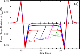
The behaviour displayed in Fig. 1 can be related to the renormalization of the electron excitations, as discussed in the next section. Here, we just remark that for the parameters used in that figure, the chemical potential is in the gap, for all the planes of the ML (see Fig. 3 in Sec. IV.2). Denoting by half the value of the Mott-Hubbard gap and by the separation between the chemical potential and the nearest band edge, we find for the leads and in the center. At low temperatures, the Fermi window is smaller than and the system behaves as an insulator. For large enough temperatures, the Fermi window exceeds and thermal fluctuations give rise to a metallic behaviour which, however, is difficult to reach by our iterative procedure. This shifting of the band edges in the central region is the mechanism that enables the system to “self-dope” and leads to many of the interesting transport phenomena that we present below.
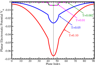
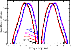
The charging error is reduced and the solution extends to higher temperatures, if the screening parameter is increased in the central part. This is illustrated in Fig. 2, where is shown for and various values of in the center. At low temperature, where the charging error is small (see the left panel), an increase of doesn’t affect the quality of the solution but at higher temperatures, where thermal fluctuations delocalize the conduction electrons and increase the metallicity of the central part, the charging error is systematically reduced as increases (see the right panel). For the data in Fig. 2, we find that the charging error at is much less than the charge in the screened-dipol layer, while at it is comparable or larger that . To reduce the charging error and obtain an acceptable solution, the screening length in the central part has to be reduced by a factor of 50 or more. In principle, the temperature dependence of the screening length should be taken into account when calculating the properties of the ML. In a fully self-consistent scheme, one would not just renormalize the electron charge but would also renormalize the dielectric constant in Poisson’s equation. One way of doing this would be to calculate the dielectric constant from the charge susceptibility which is known exactly for the Falicov-Kimball modelfreericks_2003 . However, any additional integrations make our current iterative scheme too slow, so that the renormalization of the dielectric constant requires a new numerical approach. In what follows, we restrict the calculations to constant screening parameters, in the leads and in the center and control the error by staying at relatively low temperatures.
IV.2 Local DOS
The frequency dependence of the local DOS and transport DOS is obtained, for a given set , by solving the DMFT equations on the real axis. The results obtained for the same parameters as in Fig. 1, are plotted in the left and the central panel of Fig. 3, for several typical planes of the ML. The full and dashed lines show the data obtained for and , respectively. The left panel shows the overall behaviour of for (black curve), (red), (magenta), and (blue). These data are representative for the planes in the leads far away from the interface, the planes on the two sides of the interface, and the mirror plane of the ML. Because of the symmetry with respect to the mirror plane , we have and do not have to show the data for . For , the local DOS is independent of temperature and it doesn’t change with the band shift in the central part; is a symmetric function of , which is unaffected by the interface and it is almost the same as . The same features are found for all other planes in the leads, except for the two planes next to the interface. Similarly, the local DOS on all the planes in the central part of the ML is almost the same as , except for the planes next to the interface.
The local DOS on the mirror plane and the local DOS on the leftmost plane in the leads are related by a simple shift, , where is weakly temperature dependent coefficient of the order of one. The same relationship holds for all other planes in the center, except for the planes next to the interface which are not just shifted but distorted as well. Thus, while the local DOS on the planes in semi-infinite leads are nearly the same as in the bulk, the excitations in the central part of the ML are pushed almost rigidly to higher energies. As regards the planes close to the interface, their local DOS is asymmetrically distorted with respect to the bulk, as shown in the central panel of Fig. 3. The distortion of the occupied part of is consistent with the increased number of local electrons on the plane and the distortion of the unoccupied part of is consistent with the reduced number of local electrons on plane .
The interfacing has a pronounced effect on the excitation spectrum of the ML. Unlike in the bulk, where the chemical potential is completely determined by the number of electrons, so that the local DOS of a half-filled system is symmetric with respect to the chemical potential, in the heterogeneous ML, the energy levels of electrons on the central planes are shifted with respect to the chemical potential, even though the number of electrons on most planes is the same as in the bulk. This is not surprising, since the electrons on the central planes have to adjust to the chemical potential set by the leads, while trying to maintain the local charge neutrality and minimize the potential energy. The shift of the renormalized excitation energies on the planes in the central part depends to some extent on the electrostatic potential and the real part of the self-energy but the main contribution is coming from the shift of the local chemical potential by . By tuning the offset we can bring the chemical potential arbitrarily close to the band edge and still keep most of the planes at half-filling; the charge neutrality is only broken at the planes that form an electrical dipole at the interface and give rise to the electrical potential that has a minimum (or maximum) in the center of the ML and vanishes at the edges.
For , the energy of the lowest unoccupied single-particle state is fixed by the leads (see the black curves in Fig. 1), while the energy of the highest occupied state is fixed by the central planes (see the blue curves in Fig. 1). Since the chemical potential (zero of energy) is also fixed by the leads, the upward shift of the local DOS on the central planes reduces the overall magnitude of the gap in the excitation spectrum. Furthermore, even though the chemical potential is in the gap, the separation between the chemical potential and the band edge of the lower Hubbard band is greatly reduced with respect to the bulk (see the black and blue curves in left and central panels in Fig. 3). While temperature doesn’t affect much the local DOS in the leads, an increase of temperature shifts to lower frequencies, and shifts and distorts and . The band edge of the central planes moves away from the chemical potential and we find that increases with temperature in sub-linear fashion. This temperature-dependent shift of the local DOS is caused by the temperature dependence of the Fermi factors and the renormalization of the electrochemical potential. As shown by the inset in Fig. 3, we have for and for .
The same features are observed for other choices of the parameters. For , the energy of the highest occupied single-particle state is fixed by the leads, while the energy of the lowest unoccupied state is fixed by the central planes, so an increase of reduces the gap and . A large enough brings the chemical potential into the lower or the upper Hubbard band and makes the central planes metallic. Thus, for an appropriate choice of model parameters, a small gate voltage applied to the central part can switch the system from a metallic to an insulating state. Unfortunately, our current iterative solution of the DMFT equations cannot provide the details of the transition.
If we take constant screening parameters and perform the calculations at elevated temperature for a large band offset, say, and , the chemical potential is in the conduction band and the central part is metallic. A reduction of temperature shifts the band edge across the chemical potential and gives rise eventually to a metal-insulator (MI) transition. However, for , the charging error is large and the renormalized electrical potential doesn’t vanish at the edge of the sample (see Fig.1). Close to the MI transition, which is the most interesting case for applications, we can evaluate the precise temperature dependence of the local DOS, as long as . The high-temperature DOS can only be discussed in a qualitative way, because it is obtained by the real-axis calculations which rely on the values of and . These data are produced by the imaginary-axis calculations which have, for , a large error bar. However, by studying a few cases where the iterative solution produced a small charging error, we could see that the real-axis solution exhibits qualitatively the same features as above. In other words, the real-axis results are robust with respect to the small errors in the imaginary-axis data.
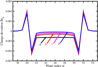
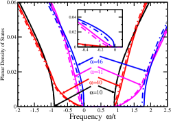
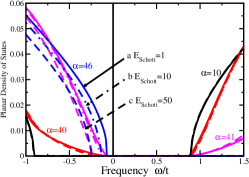
As mentioned in the previous section, the error in the charge distribution can be greatly reduced by increasing in the central part (see Fig. 2). The effect of on the local DOS is shown in the right panel of Fig. 3, where is plotted for , , in the leads, and , 10, and 50 in the central part. The data show that an increase of , at fixed temperature, brings us from the regime where and the charging error is large (curve (a), ) to the regime where and the charging error is small (curve (c), ). This feature can be used to extend the temperature range in which the transport coefficients can be computed.
The reduction of the Coulomb interaction in the leads makes the gap on the A-planes smaller than on the B-planes and further reduces
the separation between the lower band edge (set by the B-planes) and the upper band edge (set by the A-planes).
By tuning the parameters, we can transform a Mott insulator into a narrow gap semiconductor with interesting thermoelectric
properties. The deviation of the electron number from 1/2, found for and , the two planes next to the interface,
is accompanied by the deviation of and from the bulk shape, which further affects
the thermoelectric response.
IV.3 Transport function and transport coefficients
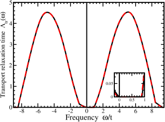
The overall features of the transport function of the ML, calculated for , and in the leads, and , and in the center, are shown in Fig. 4, where is plotted versus frequency for and . The transport gap is greatly reduced by the charge reconstruction and the ensuing long range potential which gives rise to an upward shift of the electron excitations on the central planes. In the bulk, the transport density of states of the Falicov-Kimball model is temperature-independent, when the concentration of -electrons is constant, while in a heterogeneous multilayer, we find that is weakly temperature-dependent. The low-energy part of , relevant for the transport properties, is shown in the inset of Fig. 4. The slight temperature-induced shift of , partly due to the charging error, affects the transport coefficients in a quantitative but not in a qualitative way. Unlike in heavy fermions or other strongly correlated systems with a Fermi liquid ground state, here, the slope of the transport function in the vicinity of the chemical potential is large. This has a drastic effect on the transport properties of the ML, as we now discuss.
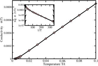
The temperature dependence of the electrical conductivity, computed for the same parameters as in Fig. 4, is plotted in the left panel of Fig. 5. At low temperatures, the conductivity exhibits an exponential decrease, , as shown in the inset. By reducing the Coulomb repulsion on the central planes (and modifying the band offset, so as to keep the chemical potential close to the band edge), the conductivity can be further enhanced. At high temperatures, shows a linear behaviour which is also found in homogeneous lightly doped Mott-Hubbard insulators, when the chemical potential is in the immediate vicinity of the band edgezlatic_2012 ; deng_2013 ; zlatic_2014 . However, the quantitative analysis of the inhomogeneous Mott-Hubbard materials is difficult because of the numerical charging error.
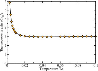
The thermopower calculated for the same parameters as in Fig. 4 is shown in the right panel of Fig. 5. At low temperatures, where the conductivity decreases, the thermopower increases rapidly. Close to the metal-insulator transition, the initial slope of the transport DOS at the chemical potential becomes very large and the thermopower of the multilayer can diverge. In the temperature range in which the electrical conductivity is linear, the thermopower is nearly constant and still very large.
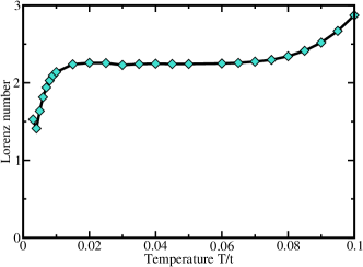
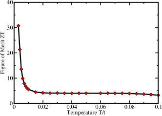
The effective Lorenz number plotted in the left panel of Fig. 6 shows at low temperatures large deviations from the universal value . Using the same parameters as in Fig. 4, and neglecting the phonon contribution, we calculated the figure-of-merit of the device, . The results are shown in the right panel of Fig. 6. In the temperature range where the thermopower becomes large and the Lorenz number deviates from its universal value, we find a large enhancement of the electronic figure-of-merit. When the device is close to the metal-insulator transition, a surprisingly large Seebeck coefficient and much enhanced figure-of-merit are observed. The enhancement is caused by the electron correlations and similar effects are not found for non-interacting electrons. The promising feature of the ML devices is the presence of the interface that can impede the phonon transport and improve the overall performance with respect to the bulk. If phonon scattering is reduced due to the mismatch of ionic masses in the leads and the central planes, the thermoelectric performance of correlated multilayers could be improved by optimizing the number of planes in the central part so as to reduce the thermal conductivity. Unlike in bulk materials, where a large power factor (given by the product of the conductivity and the square of the thermopower) is usually accompanied by large thermal conductivity, in a ML the power factor and the thermal conductivity are caused by different processes and can be tuned independently.
V Summary and outlook
This paper presents a theory of charge and heat transport parallel to the interfaces of a ABA multilayer, where A and B are half-filled Mott-Hubard insulators with large gaps in their excitation spectrum. When separated, the chemical potentials of A and B are located in the middle of their respective Mott-Hubbard gaps, while the energy bands of B are shifted relative to that of A by . In a ML, the B material is sandwiched between A leads, so as to form an ABA structure. The leftmost and the rightmost A planes are attached to a semi-infinite bulk which sets the chemical potential of the device. The excitations in the A leads are virtually unchanged by interfacing but in the central part B, they are shifted by about with respect to their position in the bulk. This gives rise to a charge redistribution and breaks the charge neutrality of the planes close to the interface. The ensuing electrical field couples self-consistently to the itinerant electrons, so that the properties of the ML crucially depend on an interplay between the on-site Coulomb forces and the long range electrostatic forces.
We model the ML by the Falicov-Kimball Hamiltonian and compute the Green’s function and the local charge on each plane by inhomogeneous DMFT. The electrical potential corresponding to that charge is calculated from Poisson’s equation and, in self-consistent calculations, it should coincide with the potential that determines the quantum states of conduction electrons. To ensure the self-consistency we recalculate the Green’s function and the charge distribution using the potential provided by Poisson’s equation and iterate this procedure to the fixed point. On the imaginary axis, this procedure yields the equilibrium charge distribution and electrostatic potentials on each plane. Once they are determined, the real-axis calculations provide the excitation spectrum and the transport function of the heterostructure.
In the leads, the electronic charge distribution and the planar DOS are almost the same as in material A, except for a few planes next to the interface, where, for , there is a charge accumulation. The local DOS on these planes deviates from the symmetric shape found in the bulk. In the central part, the local charge is also nearly the same as in material B, with the exception of the planes next to the interface, where the charge is reduced. The local DOS of the central planes retains its bulk shape but it is shifted almost rigidly by ; the exceptions are the planes with a reduced charge, where the local DOS is not just shifted but it is also distorted. The charge redistribution is mainly confined to the planes next to the A/B interfaces, where it gives rise to screened-dipole layers. Since the chemical potential and the energy of the lowest unoccupied states of the ML are set by the leads, while the energy of the highest occupied states is fixed by the central planes, and shifted by -, the interfacing reduces the gap in the transport density of states and puts the highest occupied states just below the chemical potential. In such a heterostructure, neither charge nor heat is transported perpendicular to the interface but there is a finite thermoelectric response parallel to it. This response, confined to the central part of the ML, depends sensitively on the interplay between the on-site Coulomb repulsion and the long-range electrostatic forces.
For the right choice of parameters, we find that a heterostructure built of two Mott-Hubbard insulators exhibits, in a large temperature interval, a linear conductivity and a large temperature-independent thermopower. Furthermore, we conjecture that the application of a temperature gradient perpendicular to the interface and a magnetic field parallel to the interface, say along the -axis, would give rise to the Ettinghausen voltage or the Rigi-Leduc temperature drop (thermal Hall effect) along the -axis. The experimental verification of these thermoelectric and thermomagnetic effects shouldn’t be too difficult.
Our results indicate that correlated ML’s might be quite interesting for applications. First, by tuning the band-offset, so as to bring the gap edge in
the immediate vicinity of the chemical potential, we can produce a heterostructure in which a MI transition is easily induced by a small gate voltage.
The gate voltage does not perturb much the leads, where the chemical potential is in the centre of a large gap,
but can render the central planes metallic. This switching does not involve the diffusion of electrons over macroscopic distances
and it is much faster than in ordinary semiconductors. Second, by selecting the parameters of materials A and B and tuning the number of
planes in the central part, we can reduce the phonon scattering and thermal conductivity parallel to the planes without reducing the electrical
conductivity or the thermopower. Thus, by combining strongly correlated materials with large electronic power factors but small ZT we can produce,
theoretically at least, a heterostructure with a large ZT.
Acknowledgements.
We acknowledge useful discussions and critical remarks of R. Monnier. This work is supported by the NSF grant No. EFRI-1433307. J.K.F. is also supported by the McDevitt bequest at Georgetown University. V.Z acknowledges the support by the Ministry of Science of Croatia under the bilateral agreement with the USA on the scientific and technological cooperation, Project No. 1/2014.References
- (1) S. Okamoto and A. J. Millis, Nature 428, 630 (2004); Phys. Rev. B 70, 241104(R) (2004).
- (2) L. M. Falicov and J. C. Kimball, Phys. Rev. Lett. 22, 997 (1969).
-
(3)
J. K. Freericks,
Transport in multilayered nanostructures: the dynamical mean-field theory approach,
Imperial College Press, London, Second edition 2016. - (4) J. K. Freericks, Phys. Rev. B 70, 195342 (2004);
- (5) J. K. Freericks, V. Zlatić, and A. M. Shvaika, Phys. Rev. B 75, 035133 (2007).
- (6) M. Potthoff and W. Nolting, Phys. Rev. B 60, 7834 (1999).
-
(7)
E. N. Economou,
Green’s Functions in Quantum Physics,
Springer Series in Solid-State Sciences,
Springer-Verlag Berlin Heidelberg, 2006, ISBN 978-3-642-06691-7 - (8) G. D. Mahan, Many-Particle Physics, Plenum, New York, 1981.
- (9) J. M. Luttinger, Phys. Rev. 135, A1505 (1964).
- (10) M. Jonson and G. D. Mahan, Phys. Rev. B 42, 9350 (1990).
- (11) V. Zlatić and R. Monnier, Modern theory of thermoelectricity, Oxford University Press, Oxford, 2014.
- (12) J. K. Freericks and V. Zlatić, Rev. Mod. Phys. 75, 1333 (2003).
- (13) V. Zlatić and J. K. Freericks, Phys. Rev. Lett. 109, 266601 (2012).
- (14) X. Deng, J. Mravlje, R. Žitko, M. Ferrero, G. Kotliar, and A. Georges, Phys. Rev. Lett. 110, 086401 (2013).
- (15) V. Zlatić, G. R. Boyd and J. K. Freericks Phys. Rev. B 89, 155101 (2014).