Effect of oxygen plasma on nanomechanical silicon nitride resonators
Abstract
Precise control of tensile stress and intrinsic damping is crucial for the optimal design of nanomechanical systems for sensor applications and quantum optomechanics in particular. In this letter we study the influence of oxygen plasma on the tensile stress and intrinsic damping of nanomechanical silicon nitride resonators. Oxygen plasma treatments are common steps in micro and nanofabrication. We show that oxygen plasma of only a few minutes oxidizes the silicon nitride surface, creating several nanometer thick silicon dioxide layers with a compressive stress of . Such oxide layers can cause a reduction of the effective tensile stress of a thick stoichiometric silicon nitride membrane by almost 50%. Additionally, intrinsic damping linearly increases with the silicon dioxide film thickness. An oxide layer of grown in just in a oxygen plasma almost doubled the intrinsic damping. The oxide surface layer can be efficiently removed in buffered HF.
I Introduction
Silicon nitride has become a much valued material for the fabrication of nanomechanical resonators due to its excellent mechanical and optical properties. A particularly interesting feature of silicon nitride thin films is the large intrinsic tensile stress. This stress not only defines the resonance frequency () of resonators such as strings or membranes but further dilutes intrinsic damping mechanisms, Gonzfilez and Saulson (1994); Schmid and Hierold (2008); Schmid et al. (2011); Yu, Purdy, and Regal (2012); Schmid, Villanueva, and Roukes (2016) which results in exceptionally high quality factors (). Verbridge et al. (2006); Zwickl et al. (2008); Verbridge, Craighead, and Parpia (2008); Schmid et al. (2011); Chakram et al. (2014) This has made nanomechanical silicon nitride resonators a favorite choice e.g. for cavity optomechanics experiments. Purdy, Peterson, and Regal (2013); Wilson (2012); Gavartin, Verlot, and Kippenberg (2012); Bagci et al. (2014); Thompson et al. (2008); Brawley et al. (2016)
In particular for applications in quantum optomechanics there are strong efforts underway in order to overcome the theoretically required limit of which would enable quantum experiments at room temperature. There are basically two approaches on how to improve , which are by i) optimizing damping dilution either by ”soft-clamping” of silicon nitride resonators inside phononic crystal structures, Tsaturyan et al. (2016); Ghadimi, Wilson, and Kippenberg (2017) or by increasing the tensile stress,Norte, Moura, and Gröblacher (2016) and ii) by reducing intrinsic losses.
More generally, the precise control of mechanical parameters, such as tensile stress and intrinsic damping, are of fundamental significance for the optimal design of nanomechanical sensors. In particular, the responsivity of spectrochemical sensors based on the photothermal heating of a silicon nitride resonator directly depends on the magnitude of tensile stress.Kurek et al. (2017); Andersen et al. (2016); Yamada et al. (2013); Biswas et al. (2014); Larsen et al. (2013)
In this letter we study the effect of oxygen plasma on both effective tensile stress and intrinsic loss of nanomechanical silicon nitride membrane resonators. The incineration of polymeric photoresist residues with an oxygen plasma is common practice in nano and microfabrication. Although oxygen plasma has long been known to not only effectively oxidize silicon Ligenza (1965); Kraitchman (1967); Pulfrey and Reche (1974) but also silicon nitride, Taylor et al. (1988); Kennedy et al. (1995); Kennedy, Buiu, and Taylor (1999) its effect on nanomechanical resonators has so far not been recognized.
II Methods
The experiments were done with rectangular silicon-rich (low-stress) and stoichiometric (high-stress) silicon nitride membranes. The membranes were fabricated from Si wafers coated with silicon nitride by low-pressure chemical vapor deposition (LPCVD), purchased from Hahn-Schickard-Gesellschaft für angewandte Forschung e.V. with a nominal tensile stress of and , respectively. The membranes were patterned by photolithography and dry etching of the backside silicon nitride layer and subsequently released by anisotropic KOH () wet etching all through the silicon wafer.
The oxygen plasma exposure was performed with a parallel plate STS320PC RIE plasma system from STS Systems with O2 flow and a chamber pressure of .
The vibrational analysis of the membranes was conducted under high vacuum with a laser-Doppler vibrometer (MSA-500 from Polytec GmbH). The membranes were actuated thermoelastically by focusing an amplitude modulated diode laser (, with a maximal power on the sample of ) onto the membrane rim.
The quality factors were extracted from ring-down measurements performed with a lock-in amplifier (HF2LI from Zurich Instrument). The ring-down was prepared by first driving the specific resonance mode with a phase-locked loop before stopping the actuation.
The EDX analysis was performed with a area scan directly on the membrane using an X-Max detector provided by Oxford Instruments attached to a Hitachi SU8030 scanning electron microscope.
The XPS measurements were performed with an SPECS XPS-spectrometer, equipped with a monochromatic aluminium K-alpha X-ray source (Focus 350) and a hemispheric WAL-150 analyser. Additional sample preparation was carried out using 3kV Ar+-ions from a SPECS IQ 12/38 ion sputter gun. The surface composition analysis was supported by simulation of electron spectra for surface analysis (SESSA) software.Smekal, Werner, and Powell (2005)
The thin film thickness was measured with a Filmetrics F20-UVX thin film analyzer.
III Results & Discussion
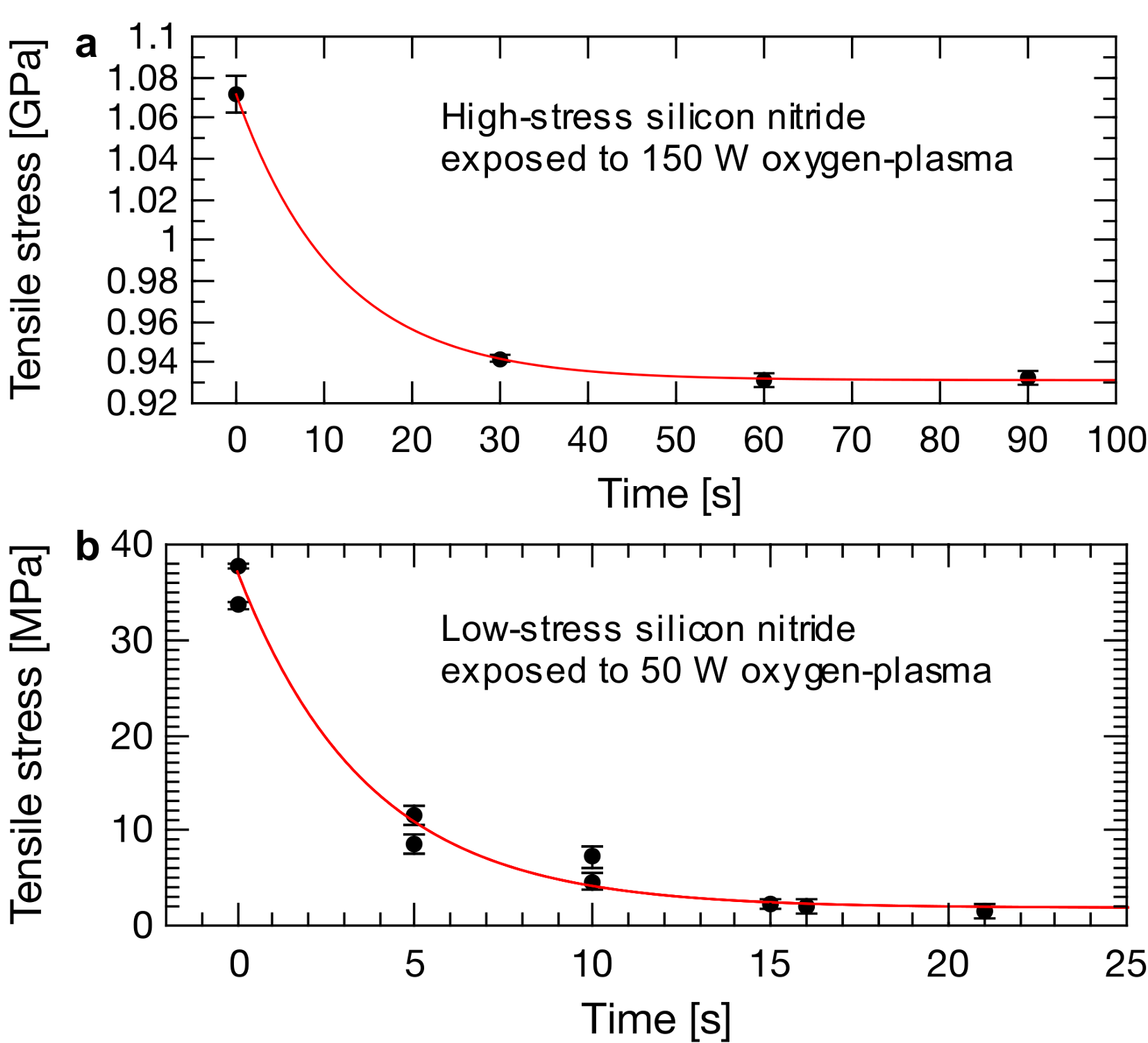
Figure 1 shows the tensile stress of high-stress and low-stress silicon nitride membranes for an increasing time in oxygen plasma. The tensile stress was extracted from the eigenfrequency model for membranes Schmid, Villanueva, and Roukes (2016)
| (1) |
with length , mode numbers and , and assuming a mass density of . Comparisons with an extended plate model have shown that the ideal membrane model (1) holds true for all analysed membranes under tensile stress. For both types of membranes, tensile stress drops exponentially with plasma exposure time. The intrinsic tensile stress in the high-stress silicon nitride membranes dropped by almost when shortly exposed to an oxygen plasma of (see Figure 1a). For low-stress silicon nitride membranes the initial tensile stress reduced to almost zero for an exposure to only (see Figure 1b). When treating the low-stress silicon nitride with oxygen plasma the stress even reversed from tensile to compressive, as can be seen from microscope images shown in Figure 2a.
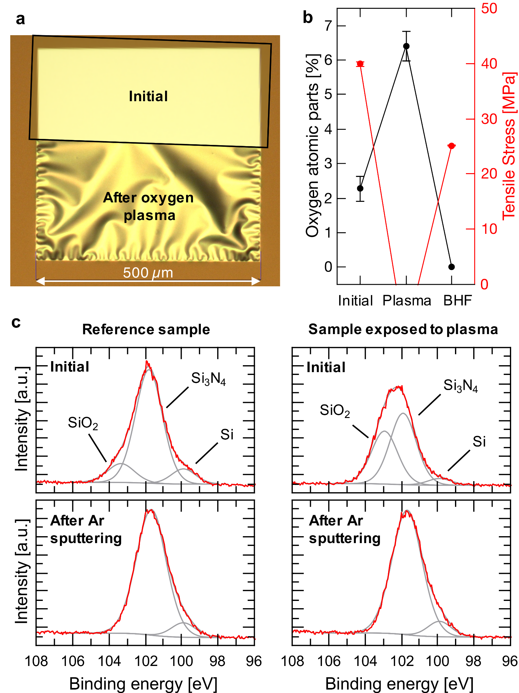
Figure 2b presents the atomic composition and tensile stress of low-stress silicon nitride membranes measured i) initially, ii) after a exposure to oxygen plasma, and iii) after a bath in buffered hydrofluoric acid (BHF). As mentioned before, oxygen plasma resulted in compressive stress, clearly visible by the ripples in the membrane in Figure 2a, and an increased oxygen content. A subsequent dip in buffered HF (BHF) recovered the tensile stress. The same recovery was also found for high-stress silicon nitride membranes, whose stress reached 96% of the initial value after a dip in BHF (data not shown). This is clear evidence that the stress reduction is caused by a surface layer with compressive stress and that is removable in BHF. It is known that oxygen plasma not only creates a compressive silicon dioxide layer in silicon substrate,Pulfrey and Reche (1974) but it also efficiently oxidises LPCVD silicon nitride thin films.Taylor et al. (1988) The rise in atomic oxygen content after plasma seen in Figure 2b can be attributed to the creation of such an oxidation layer.
From previous work it appears that the oxygen from the plasma substitutes the nitrogen in the silicon nitride film. In detail, these oxygen plasma grown silicon dioxide films feature a vertical gradient in composition ranging from i) a silicon dioxide layer at the surface, due to a loss of all nitrogen atoms into the plasma, to ii) pure silicon nitride at the interface. Buiu et al. (1998); Kennedy, Buiu, and Taylor (1999); Kennedy et al. (1995) Evidence of the growth of such a silicon dioxide layer was obtained by XPS analysis, which revealed that the surface of the plasma induced oxidation layer indeed is fully depleted of nitrogen. Figure 2c presents the chemical state analysis of the Si 2p region a silicon nitride sample before (reference sample) and after oxygen plasma exposure. Deconvolution of these Si 2p peaks shows that both samples exhibit an SiO2 (103.5 eV) component in addition to Si3N4 (101.7 eV). However, the plasma treated silicon nitride shows a significant SiO2-related component, representing a substantial SiO2 film, with a thickness of several nm. In contrast to the faint SiO2 signature of the reference sample, which can be assigned to a few monolayers of native SiO2 at the silicon nitride surface. After sputtering of the sample surface with Ar ions, the SiO2 related peaks disappeared completely for both samples.
In the plasma oxidation process, the volume of Si3N4 molecules of 77.5 Å3 (calculated assuming a mass density of 3000 kg/m3) grows to the volume of three SiO2 molecules of 45.5 Å3 each (assuming a mass density of 2200 kg/m3). In the case of planar growth the consumed Si3N4 is replaced by a SiO2 film that is theoretically 1.77 thicker, which has been verified with electron microscope images of oxidised silicon nitride surfaces.Taylor et al. (1988) The growth of SiO2 leads to a one-dimensional unrelaxed strain of , which would result in an enormous compressive stress of . This is of the same order of magnitude of the initial stress building up during silicon oxidation.Sutardja and Oldham (1989) However, this enormous compressive stress is expected to relax to a magnitude close to the compressive strength of amorphous silicon dioxide of approximately .
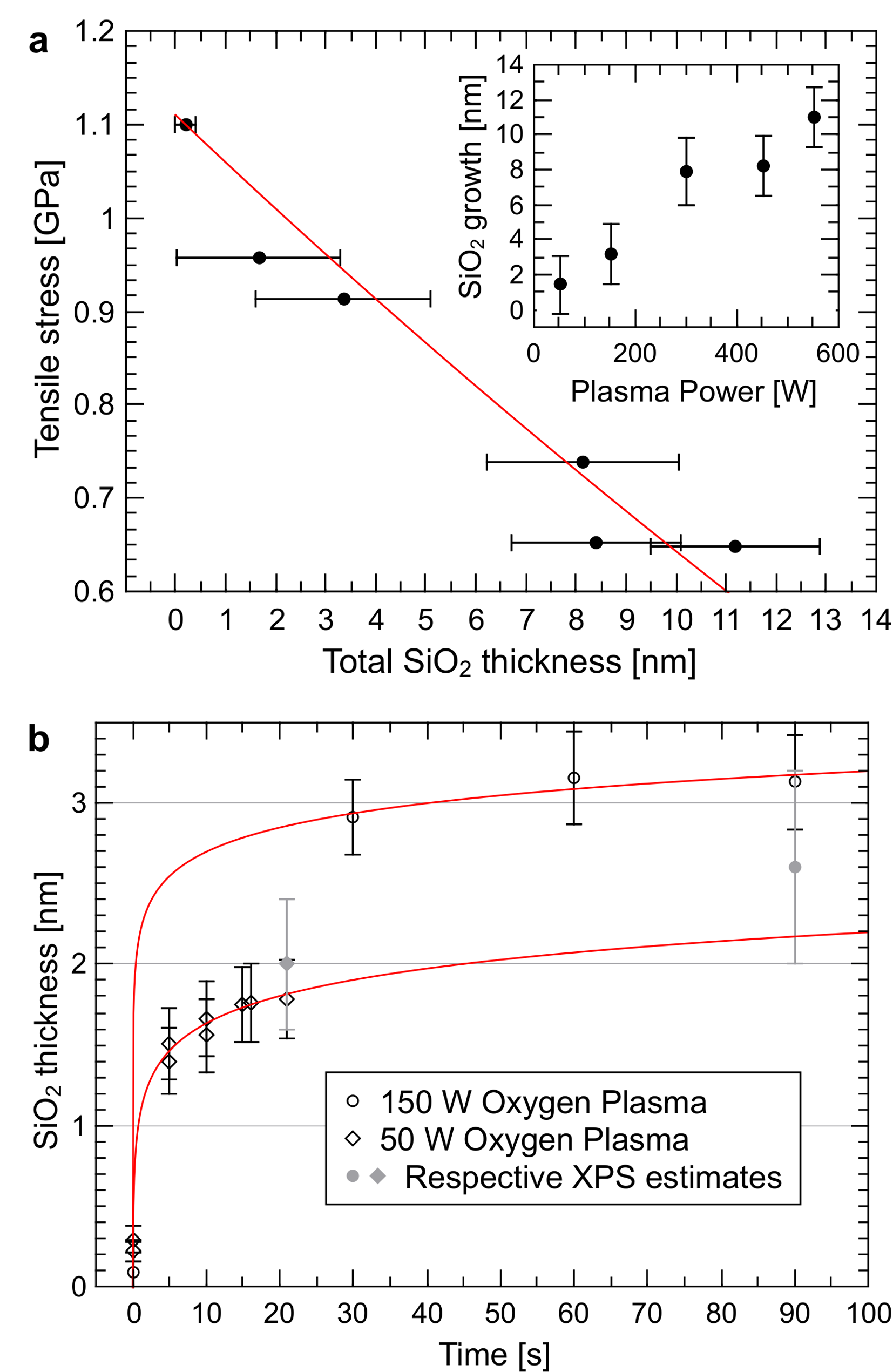
In order to estimate the effective compressive stress of the silicon dioxide layer, high-stress silicon nitride membranes were oxidised with various plasma powers. Afterward the grown SiO2 was removed in BHF. The SiO2 layer thickness was then calculated from the reduction of the silicon nitride film thickness (see inset of Figure 3a), taking into account the volume increase during oxidation and the BHF etch-rate of the silicon nitride. Figure 3a shows the tensile stress , obtained from measured membrane resonance frequencies, versus the measured oxide film thickness. The effective stress in the silicon nitride membrane can be modelled as the arithmetic mean of the tensile stress of the silicon nitride (of thickness ) and the compressive stress of the silicon dioxide layer (of thickness )
| (2) |
Fitting the model (2) to the data in Figure 2a allows the extraction of a compressive stress of the SiO2 film of . The measured stress is of the expected magnitude of the compressive strength of amorphous silicon dioxide.
With the gained value for the compressive stress , it is now possible to estimate the oxide film thickness based on the measured effective stress . Figure 3b plots the estimated SiO2 thickness of the silicon dioxide layer as a function of oxygen plasma time for the two samples presented in Figure 1. The same samples have been analysed with XPS and quantitative results have subsequently been compared with simulations varying the SiO2 layer thickness, and the obtained thickness estimates match well with the estimated values from the effective tensile stress by means of (2). It has been shown that oxygen plasma induced oxide growth at room temperature shows logarithmic behavior.Kim et al. (1996) The same behavior seems to hold true for the oxygen plasma grown from silicon dioxide thin films, as can be seen by the logarithmic fits shown as red lines.
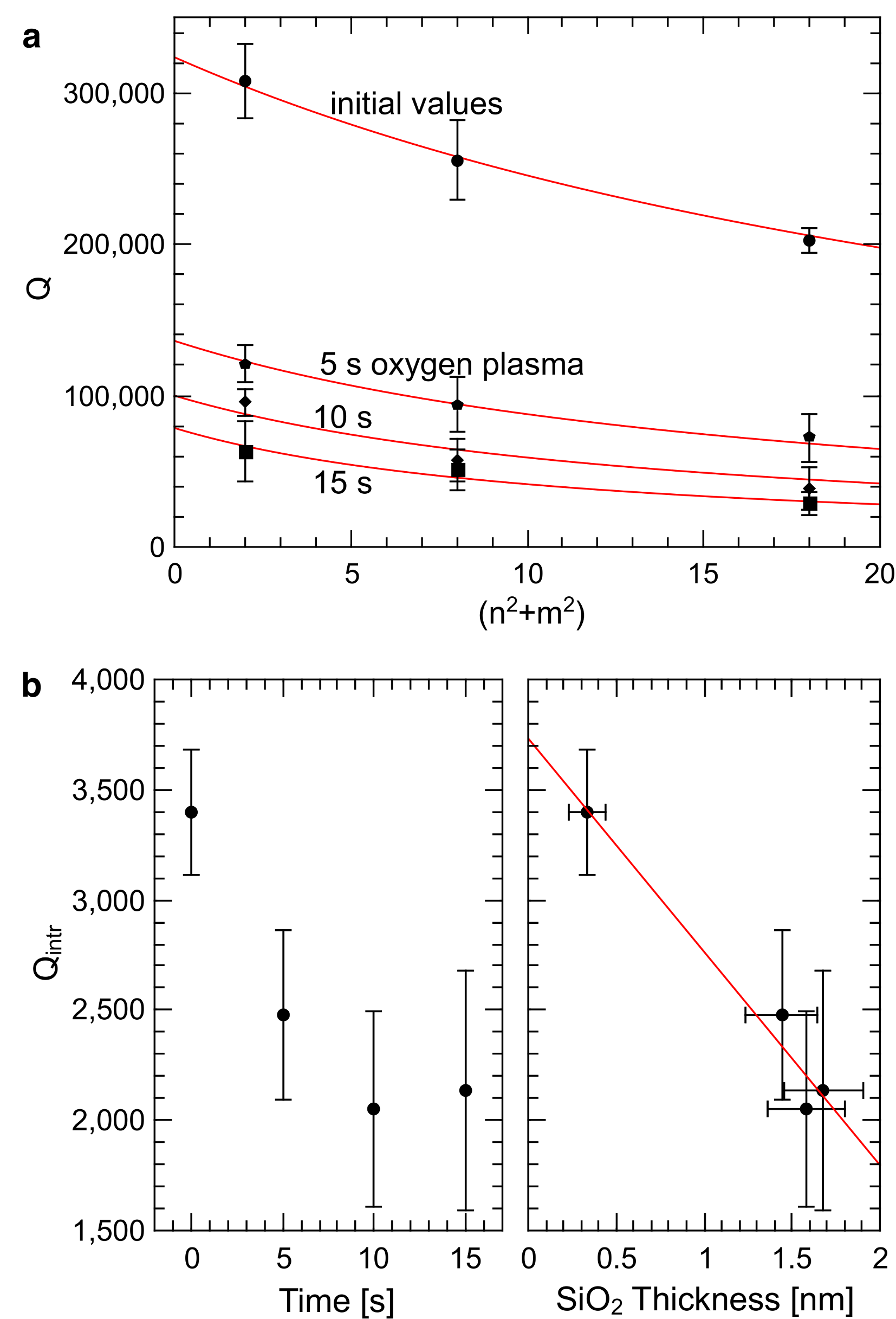
In order to study the effect of oxygen plasma on intrinsic losses, the quality factor of low-stress silicon nitride membranes was measured, as presented in Figure 4a. The low tensile stress in these membranes produce a sufficient decoupling from the chip frame thereby minimizing radiation losses.Villanueva and Schmid (2014) Hence, the measured quality factors are exclusively limited by intrinsic damping, which is further confirmed by the fact that the measured values for each treatment step follow the prediction (red curves) from the damping dilution model (3) for intrinsic loss (1/) in membranesYu, Purdy, and Regal (2012); Schmid, Villanueva, and Roukes (2016)
| (3) |
The intrinsic loss (1/) was then extracted by correcting the measured quality factor values for the stress induced damping dilution effect (3) assuming a Young’s modulus of for silicon-rich silicon nitride.Guo and Lal (2003) The respective intrinsic quality factors for the different plasma exposure times are plotted in Figure 4b, together with the correlation to the estimated silicon dioxide film thickness. Apparently, intrinsic losses increase with oxygen plasma exposure. The comparison of with the estimated oxide thickness shows a linear correlation. This suggests that the increased loss can be attributed to the growth of the silicon dioxide surface layer, which has larger intrinsic damping than silicon nitride.Southworth et al. (2009) The magnitude of the initial value matches the general value found for surface loss in silicon nitride.Villanueva and Schmid (2014)
IV Conclusion
Silicon nitride structures with a thickness of only are highly sensitive to oxygen plasma. Even short exposures cause a significant decreases in tensile stress and an increase in intrinsic loss. Both effects can be attributed to the plasma-induced oxidation of the silicon nitride surface. We found that the created silicon dioxide film on the silicon nitride surface has a compressive stress of , which is probably limited by the layers’ own compressive strength.
This relatively large stress counteracts the intrinsic tensile stress in LPCVD silicon nitride, leading to a significant drop of the intrinsic stress and hence in the resonance frequency. Oxygen plasma exposure of nanomechanical silicon nitride resonators can reduce the tensile stress by several hundreds of MPa, which for low-stress silicon nitride structures can even cause a total reversal of the effective stress from tensile to compressive. Hence it is an interesting tool which allows a precise post-fabrication control of tensile stress.
Additionally, the plasma grown silicon dioxide layer significantly increases energy loss in nanomechanical silicon nitride resonators. Hence, for applications where a maximum tensile stress as well as minimum intrinsic damping is desired, the silicon dioxide layer and its deteriorating effects can fully be removed by a quick BHF dip.
Since an oxygen plasma also oxidizes silicon surfaces, similar effects as observed for silicon nitride resonators will likely occur in nanomechanical structures made from silicon.
Acknowledgements.
We thank Sophia Ewert and Patrick Meyer for the cleanroom support. This project has received funding from the European Research Council (ERC) under the European Union s Horizon 2020 research and innovation program (grant agreement - 716087 - PLASMECS).References
- Gonzfilez and Saulson (1994) G. I. Gonzfilez and P. R. Saulson, Journal of the Acoustical Society of America 96, 207 (1994).
- Schmid and Hierold (2008) S. Schmid and C. Hierold, Journal of Applied Physics 104, 093516 (2008).
- Schmid et al. (2011) S. Schmid, K. D. Jensen, K. H. Nielsen, and A. Boisen, Physical Review B 84, 165307 (2011).
- Yu, Purdy, and Regal (2012) P.-L. Yu, T. Purdy, and C. A. Regal, Physical Review Letters 108, 083603 (2012).
- Schmid, Villanueva, and Roukes (2016) S. Schmid, L. G. Villanueva, and M. L. Roukes, Fundamentals of Nanomechanical Resonators, 1st ed. (Springer International Publishing, 2016).
- Verbridge et al. (2006) S. S. Verbridge, J. M. Parpia, R. B. Reichenbach, L. M. Bellan, and H. G. Craighead, Journal of Applied Physics 99, 124304 (2006).
- Zwickl et al. (2008) B. M. Zwickl, W. E. Shanks, A. M. Jayich, C. Yang, B. Jayich, J. D. Thompson, and J. G. E. Harris, Applied Physics Letters 92, 103125 (2008).
- Verbridge, Craighead, and Parpia (2008) S. S. Verbridge, H. G. Craighead, and J. M. Parpia, Applied Physics Letters 92, 013112 (2008).
- Chakram et al. (2014) S. Chakram, Y. S. Patil, L. Chang, and M. Vengalattore, Physical Review Letters 112, 127201 (2014).
- Purdy, Peterson, and Regal (2013) T. P. Purdy, R. W. Peterson, and C. A. Regal, Science 339, 801 (2013).
- Wilson (2012) D. J. Wilson, Cavity Optomechanics with High-Stress Silicon Nitride Films, Ph.D. thesis, California Institute of Technology (2012).
- Gavartin, Verlot, and Kippenberg (2012) E. Gavartin, P. Verlot, and T. J. Kippenberg, Nature Nanotechnology 7, 509 (2012).
- Bagci et al. (2014) T. Bagci, A. Simonsen, S. Schmid, L. G. Villanueva, E. Zeuthen, J. Appel, J. M. Taylor, A. Sørensen, K. Usami, A. Schliesser, and E. S. Polzik, Nature 507, 81 (2014).
- Thompson et al. (2008) J. D. Thompson, B. M. Zwickl, A. M. Jayich, F. Marquardt, S. M. Girvin, and J. G. E. Harris, Nature 452, 72 (2008).
- Brawley et al. (2016) G. a. Brawley, M. R. Vanner, P. E. Larsen, S. Schmid, A. Boisen, and W. P. Bowen, Nature Communications 7 (2016), 10.1038/ncomms10988, arXiv:1404.5746 .
- Tsaturyan et al. (2016) Y. Tsaturyan, A. Barg, E. S. Polzik, and A. Schliesser, , 1 (2016), arXiv:1608.00937 .
- Ghadimi, Wilson, and Kippenberg (2017) A. H. Ghadimi, D. J. Wilson, and T. J. Kippenberg, Nano Letters ASAP (2017), 10.1021/acs.nanolett.7b00573, arXiv:1603.01605 .
- Norte, Moura, and Gröblacher (2016) R. A. Norte, J. P. Moura, and S. Gröblacher, Physical Review Letters 116, 1 (2016), arXiv:1511.06235 .
- Kurek et al. (2017) M. Kurek, M. Carnoy, P. E. Larsen, L. H. Nielsen, O. Hansen, T. Rades, S. Schmid, and A. Boisen, Angewandte Chemie International Edition , 3901 (2017).
- Andersen et al. (2016) A. J. Andersen, S. Yamada, P. Kumar E.K., T. L. Andresen, A. Boisen, and S. Schmid, Sensors and Actuators B: Chemical 233, 667 (2016).
- Yamada et al. (2013) S. Yamada, S. Schmid, T. Larsen, O. Hansen, and A. Boisen, Analytical Chemistry 85, 10531 (2013).
- Biswas et al. (2014) T. S. Biswas, N. Miriyala, C. Doolin, X. Liu, T. Thundat, and J. P. Davis, Analytical chemistry 86, 11368 (2014).
- Larsen et al. (2013) T. Larsen, S. Schmid, L. G. Villanueva, and A. Boisen, ACS Nano 7, 6188 (2013).
- Ligenza (1965) J. R. Ligenza, Journal of Applied Physics 36, 2703 (1965).
- Kraitchman (1967) J. Kraitchman, Journal of Applied Physics 38, 4323 (1967).
- Pulfrey and Reche (1974) D. Pulfrey and J. Reche, “Preparation and properties of plasma-anodized silicon dioxide films,” (1974).
- Taylor et al. (1988) S. Taylor, W. Eccleston, J. Ringnalda, D. M. Maher, D. J. Eaglesham, C. J. Humphreys, and D. J. Godfrey, Journal de Physique 49, 393 (1988).
- Kennedy et al. (1995) G. P. Kennedy, S. Taylor, W. Eccleston, W. M. Arnoldbik, and F. H. M. Habraken, Microelectronic Engineering 28, 141 (1995).
- Kennedy, Buiu, and Taylor (1999) G. P. Kennedy, O. Buiu, and S. Taylor, Journal of Applied Physics 85, 3319 (1999).
- Smekal, Werner, and Powell (2005) W. Smekal, W. S. M. Werner, and C. J. Powell, Surface and Interface Analysis 37, 1059 (2005).
- Buiu et al. (1998) O. Buiu, G. Kennedy, M. Gartner, and S. Taylor, IEEE Transactions on Plasma Science 26, 1700 (1998).
- Sutardja and Oldham (1989) P. Sutardja and W. Oldham, IEEE Transactions on Electron Devices 36, 2415 (1989).
- Kim et al. (1996) K. Kim, M. H. An, Y. G. Shin, M. S. Suh, C. J. Youn, Y. H. Lee, K. B. Lee, and H. J. Lee, Journal of Vacuum Science & Technology B 14, 2667 (1996).
- Villanueva and Schmid (2014) L. G. Villanueva and S. Schmid, Physical Review Letters 113, 1 (2014), arXiv:1405.6115 .
- Guo and Lal (2003) H. Guo and A. Lal, Journal of Microelectromechanical Systems 12, 53 (2003).
- Southworth et al. (2009) D. R. Southworth, R. A. Barton, S. S. Verbridge, B. Ilic, A. D. Fefferman, H. G. Craighead, and J. M. Parpia, Physical review letters 102, 225503 (2009).