Radiation damage caused by cold neutrons in boron doped CMOS active pixel sensors
Abstract
CMOS Monolithic Active Pixel Sensors (MAPS) are considered as an emerging technology in the field of charged particle tracking. They will be used in the vertex detectors of experiments like STAR, CBM and ALICE and are considered for the ILC and the tracker of ATLAS. In those applications, the sensors are exposed to sizeable radiation doses.
While the tolerance of MAPS to ionizing radiation and fast hadrons is well known, the damage caused by low energy neutrons was not studied so far.
Those slow neutrons may initiate nuclear fission of 10B dopants found in the B-doped silicon active medium of MAPS. This effect was expected
to create an unknown amount of radiation damage beyond the predictions of the NIEL (Non Ionizing Energy Loss) model for pure silicon.
We estimate the impact of this effect by calculating the additional NIEL created by this fission. Moreover, we show first measured data for CMOS sensors which were irradiated with cold neutrons. The empirical results contradict the prediction of the updated NIEL model both, qualitatively and quantitatively: The sensors irradiated with slow neutrons show an unexpected and strong acceptor removal, which is not observed in sensors irradiated with MeV neutrons.
1 Introduction
The ultra-light and highly granular CMOS Monolithic Active Pixel Sensors (MAPS) are considered as sensor technology for various charged particle detectors like the micro vertex detector (MVD) of the CBM experiment at FAIR[1]. A dedicated R&D program of the PICSEL group of IPHC Strasbourg and the IKF Frankfurt aims to match their radiation tolerance to the requirements of the CBM-MVD, which amount and 3 Mrad per year of operation [2].
A 3T-pixel of a MAPS is shown in Figure 1. It consists of three B-doped silicon layers: The highly doped substrate, a thick, moderately doped epitaxial layer and a thin, highly doped P-well with N-well implants. The partially depleted epitaxial layer serves as the active medium of the sensor. The N-well and the epitaxial layer form its diode. Free electrons, which were excited by particles impinging the epitaxial layer, diffuse in the epitaxial layer unless they reach the depleted volume of the diodes. The collected electrons discharge the parasitic capacity of the diode. The related voltage drop is buffered by a source follower and discriminated with an ADC/discriminator (not shown). The pixel capacity is recharged by opening the reset transistor.
The tolerance of MAPS to non-ionizing radiation damage has regularly been studied with fast reactor neutrons in accordance with the NIEL (Non-Ionizing-Energy-Loss) model [3]. This model assumes that the crystal damage caused by massive particles scales with their non-ionizing energy loss. The energy deposit is normalized to multiples of the one of neutrons (Neq). Tables on the energy dependent NIEL of neutrons in pure silicon as plotted in Figure 2(b) were used to estimate the required radiation tolerance of the sensors of the CBM-MVD.
Additional NIEL is generated in B-doped silicon by a neutron induced fission of the boron dopants (n + 10B Li + 4He + 2.8 MeV). First radiation studies carried out with n-p-n transistors realized in the DMILL process [4, 5] suggest that this additional damage is sizable and may exceed the one expected from 1 MeV neutrons while it is considered as negligible in the standard NIEL model. To exclude a possible impact of thermal neutrons to the safe operation of the CBM-MVD, we studied the radiation damage caused by thermal neutrons in MAPS. This was done by estimating the additional radiation damage caused by the fission within the framework of the NIEL model. Moreover, we irradiated a MAPS prototype with cold neutrons and tested it for radiation damage.
2 NIEL caused by neutron induced Boron fission, a theoretical estimate
Natural boron contains 19.8% 10B and 80.2% 11B. The neutron capture cross section of 11B is negligible, while the one of 10B amounts for thermal neutrons ( eV, see figure 2(a)). In the following, we assume that manufacturers of standard CMOS electronics use natural boron. The number of boron fissions per volume, , for monoenergetic neutrons with an energy is given by:
| (2.1) |
Here, is the integrated neutron flux in units of , the doping concentration. I=19.8% is the isotopic factor of 10B and represents the energy dependent cross-section for the n + 10B Li + 4He + 2.8 MeV reaction. The energy of the impinging neutron and the frequent formation of a -ray with 478 keV is neglected. The 2.8 MeV fission energy provides and to the fission products. The range of the ions was simulated with SRIM (Stopping Power of Ions in Matter) [6] and amounts in silicon to and for He and Li, respectively. Most energy is deposited in a Bragg peak at the end of the ion trajectory.
The ions deposit most of their energy by ionizing interactions. To estimate the non-ionizing energy deposit, we simulated the number of crystal vacancies caused by the ions with SRIM and compared them with the related number for 10 MeV protons, which have a known hardness factor. By doing so, we assume that the indicated number of vacancies scales with the hardness factor of the particles. This was tested for several proton energies between 100 keV and 10 MeV and a good agreement with a standard deviation of 7% was observed. According to the simulation, the helium and lithium ions create in average 280 and 510 vacancies per ion, respectively. The sum amounts vacancies per boron fission. For 10 MeV protons (hardness factor Neq [7]) penetrating a 10 silicon target, vacancies per cm trajectory were indicated.
According to the NIEL model, the number of vacancies scales with the non-ionizing energy deposit. Provided the SRIM simulation is valid, one may compare the number of vacancies to estimate the NIEL of the fission products in units of . One obtains:
| (2.2) |
The fission induced hardness factor for neutrons with a given energy is:
| (2.3) |
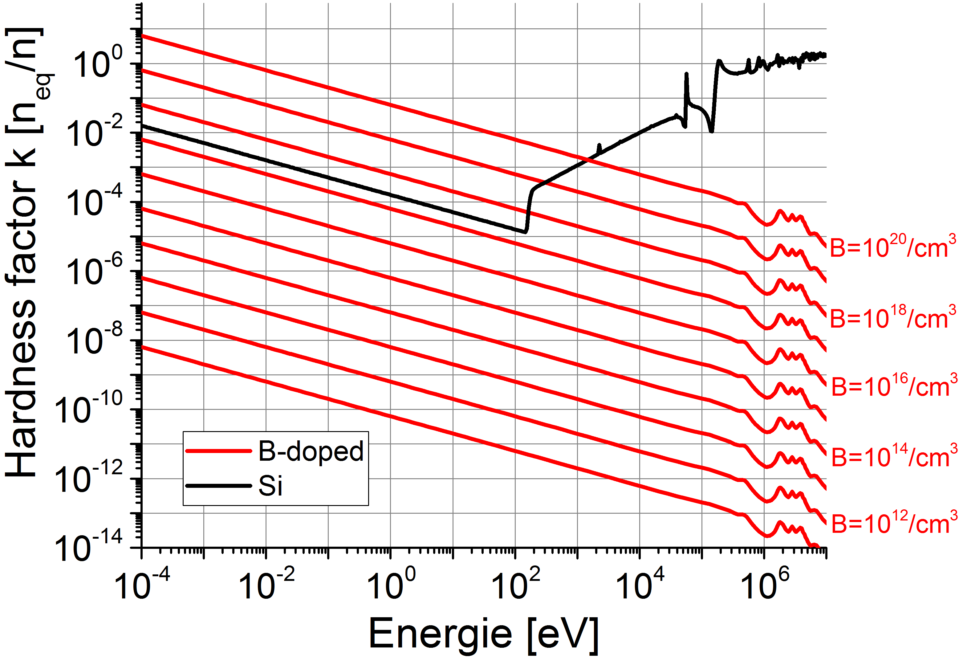
Figure 2(b) which compares of different doping concentrations with the hardness factor for pure silicon. One observes that the NIEL caused by the boron fission reaches the NIEL expected for pure silicon starting from doping concentrations slightly above .
The epitaxial layers of typical CMOS sensors have a doping concentration below , the wells may reach , and the substrate shows typically a doping of . Therefore, in first order, boron is not expected to cause additional radiation damage in the MAPS. However, fission ions created in the highly doped structures may travel toward the epitaxial layer and cause bulk damage there. According to previous studies [13], this bulk damage may increase the leakage currents of the diodes and moreover reduce the charge collection efficiency of the sensor.
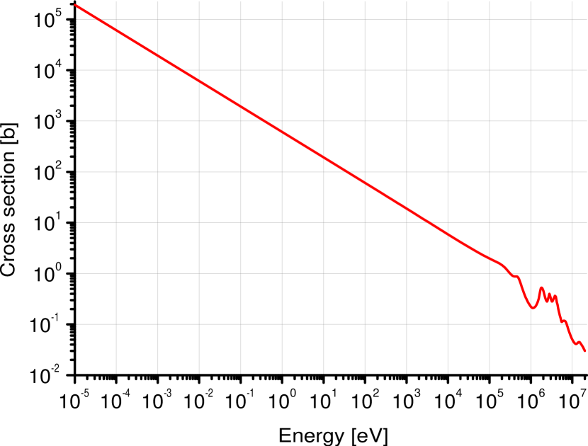
(a) Cross section for the n+10B 7Li+4He +X reaction. Data from [8].
(b) Estimated hardness factor of neutrons impinging pure silicon (black, data from [9]), predicted damage due to boron fission (red). The prediction is not supported by data, see text.
3 Effects of cold neutrons on CMOS sensors
To investigate the effects of boron fission, we obtained MIMOSA-19 sensors from the PICSEL group of IPHC Strasbourg and irradiated them at the FRM II research reactor in Garching. The sensors were manufactured in a 0.35 CMOS technology and feature a 14 thick epitaxial layer with an anticipated B-doping of few . The 3T-pixels with 12x12 pitch have L-shaped diodes with 39.6 surface. The anticipated doping of the substrate of the P-Well is .
The chips were irradiated at the MEDAPP beam line [10] with fast neutrons (a direct fission spectrum with (peak), hardness factor for pure Si Neq, for 99% of all neutrons). Unwanted -rays caused an ionizing dose of per . Other sensors were irradiated at the PGAA beam line [11] with cold neutrons (average energy corresponding222As obtained from folding the spectrum given in [12] with hardness factors according to [9]. to =0.003 Neq) and an unknown ionizing dose. The irradiation was done at room temperature. Despite the sensors remained unpowered during irradiation, the ionizing radiation damage is considered to determine the leakage currents after irradiation.
The sensors were bonded, illuminated with X-ray sources (55Fe, 109Cd) and their amplitude spectra were recorded according to our standard protocol (see [13]). The summed amplitude spectrum of groups four pixels of X-ray clusters are known to provide a good relative measure of the charge collection efficiency (CCE) of neutron irradiated sensors. The CCE of MAPS with 3T-pixel was previously found not to be significantly modified by ionizing radiation damage (see e.g. [13], section 5.3.3 and 5.3.4.3). Comparing CCE measurements done with 55Fe and 109Cd was confirmed to be appropriate due to the linear response of the sensor.
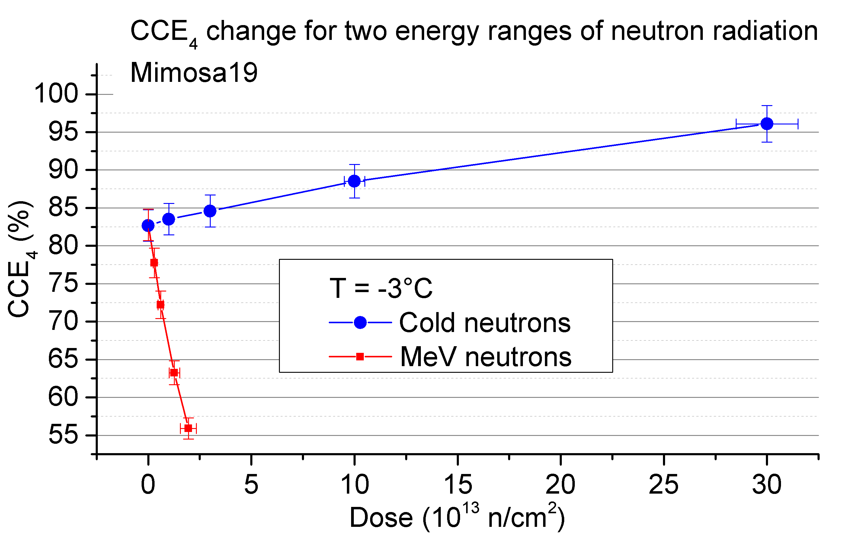
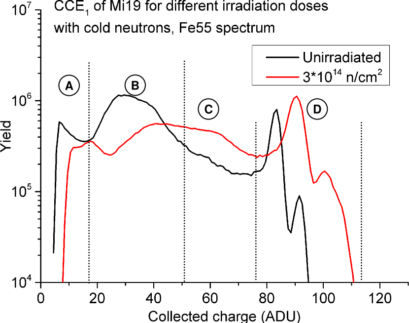
The results of the study are displayed in Figure 3(a). The sensors irradiated at MEDAPP display a decrease of the average CCE with increasing radiation dose, which matches the results of other studies (e.g. [15]). In the sensors irradiated at PGAA, one observes an unexpected increase of the CCE. The slope of the CCE does thus depend on the neutron energy, what cannot be explained within the NIEL model.
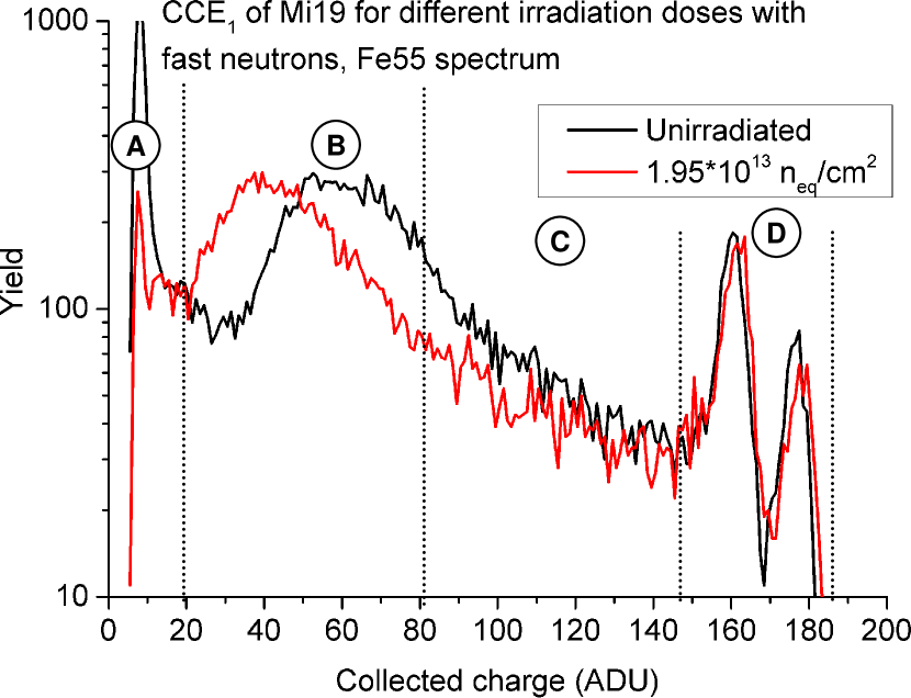
In order to obtain a closer understanding of the effect, we analyzed the amplitude spectra of the sensors in detail. For this purpose, we employed spectra, which show the charge deposited in the seed pixel of the hit clusters. Such a spectrum (see Figure 3(b)) may be subdivided into four regions: Region (b) reflects X-rays, which hit the non-depleted epitaxial layer. Region (c) shows the hits in an intermediate zone nearby the depleted volume of the diodes. Region (d) shows the response of the sensor to direct hits in the depleted volume. The low energy region (a) can be ignored here.
In sensors irradiated at MEDAPP with fast neutrons (Figure 3(b)), one observes region (d) to remain unchanged within uncertainties after irradiation. Therefore, the properties of the depleted volume is considered as unchanged. The peak in (b) is shifted to lower values after irradiation, which indicates a partial recombination of diffusion signal charge due to bulk damage.
For the sensor irradiated at PGAA with cold neutrons (Figure 3(c)), region (b) is mostly depleted after irradiation and the remaining peak is shifted to higher values. Most of the entries missing in (b) are found in region (c). This indicates that the pixel diode improved its CCE for charge created in the nearby epitaxial layer and that there is no significant charge recombination after irradiation. The number of entries in region (d) increases significantly after irradiation. This is interpreted as an extension of the depleted volume of the pixel diode, which explains the previous observation. Moreover, the peak is shifted toward higher values. This suggests a reduced diode capacity as caused by an extended depleted volume.
The findings are not explained by a radiation induced modification of the gain of the amplifiers of the readout chain. A linear modification would shift the peaks in (d) as observed. However, the number of entries in the peaks should remain constant, which does not match the observations. An radiation induced, non-linear modification of the amplifier response curve is also not suited to explain the modified shape of the spectrum. It this scenario, the peaks in region (d) would be smeared out333The dark signal of the pixels (before performing correlated double sampling) is widely spread. A non-linear amplifyer response would thus turn into a sizeable spread of gain from pixel to pixel. The formation of the peaks observed requires the pixels to show an identical gain., which is not observed.
A plausible explaination considers a strong, radiation induced acceptor removal, which reduces the doping of the epitaxial layer and such increases the size of the depleted zone of the diode. The numbers of entries in the peaks in region (d) increases by a factor slightly above two. For flat PN-junctions, this would turn into a drop in doping by a rough factor of five.
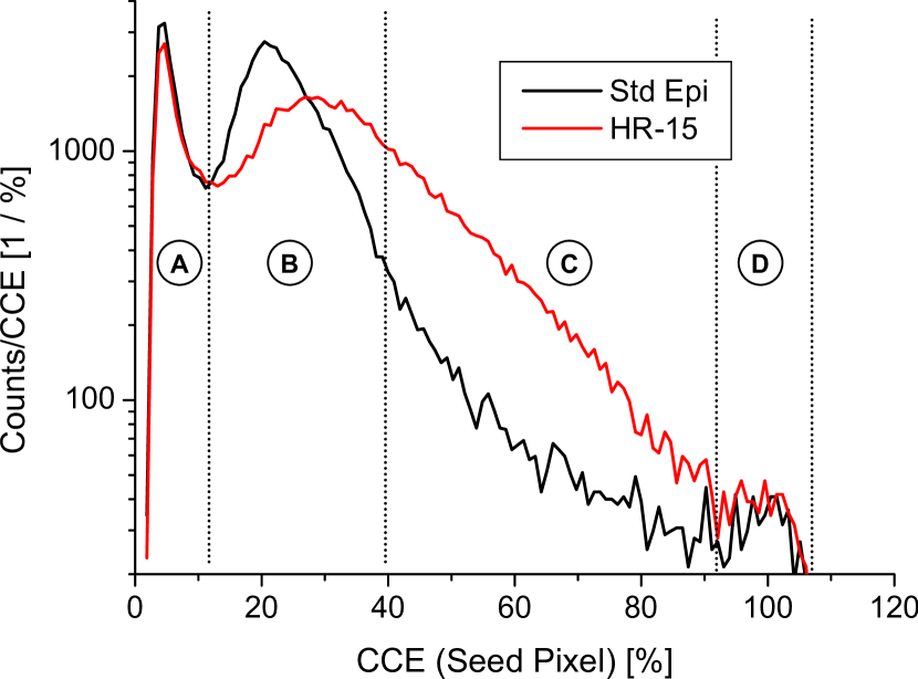
The hypothesis of an acceptor removal is supporting the results of previous studies [15], which compared the spectra of MIMOSA-26 sensors with known highly (Std Epi, few ) and lowly doped (HR-15, few ) epitaxial layer [14]. As shown in Figure 3(d), the reduced doping created similar modifications of the amplitude spectrum in region (b) and (c). A significant increase of the depleted volume -region (d)- was not observed with MIMOSA-26, which was interpreted as a consequence of the small size and depletion voltage of the diode of this chip.
Note that, unless isotope enriched boron was used for doping, the strong acceptor removal observed cannot be explained with the physical destruction of the 10B atoms alone. This is as natural boron contains 80.2% of 11B, which shows only a small fission cross section and thus should remain mostly stable. We investigated if transmutation N-doping (a phosphorus production by thermal neutrons in silicon, n + 30Si P + e + ) could explain our findings. The number of 30P atoms produced was estimated to about three orders of magnitude below the number of missing acceptors, which seems to exclude this scenario. It might be worth speculating, if the slow ions created in the 10B-fission may each produce numerous traps, which act as effective N-dopands.
4 Summary and conclusion
The response of B-doped silicon sensors to thermal radiation has been studied theoretically and experimentally. Computations based on the NIEL model predict that the neutron induced fission of boron dopands in silicon (n + 10B Li + 4He + 2.8 MeV) will add significant bulk damage in case the doping concentration exceeds . Ions being created in the P-wells and the substrate were expected to damage the active volume of MAPS, which is by itself too lowly doped to obtain significant additional damage. We expected therefore that cold neutrons would reduce the charge collection efficiency (CCE) of sensors exposed to cold neutrons to some extent. This prediction is proven wrong by our observations made on sensors irradiated with cold neutrons. We observe an excessive acceptor removal, which is not observed in sensors irradiated with fast neutrons, and increases the CCE of the sensor. This suggests that cold and fast neutrons generate traps with different properties. The traps created by the fast neutrons do dominantly reduce the charge carriers lifetime. The traps created by thermal neutrons create dominantly a substantial acceptor removal and the reduction of charge carriers lifetime is either absent or compensated by the faster charge collection found in lowly-doped epitaxial layers.
We conclude that the sensor reacts in a fundamentally different way to slow and fast neutrons. Therefore, the NIEL model appears not suited to parametrize or predict the radiation damage induced by slow neutrons to our sensor. As MIMOSA-19 does not allow for a direct access of the doping concentration, e.g. by C-V measurements of the diode, our findings remain somewhat qualitative. We recommend therefore to repeat the study with suited test structures.
Acknowledgments
This work was supported by HIC for FAIR, GSI and the BMBF (06FY90991, 05P12RFFC7).
References
- [1] M. Deveaux et al., The silicon detector systems of the Compressed Baryonic Matter experiment, PoS Vertex2013 (2013) 009
- [2] M. Deveaux et al., Development of CMOS Monolithic Active Pixel Sensors for the ALICE-ITS Outer Barrel and for the CBM-MVD, PoS (Vertex2015) 045
- [3] A. Vasilescu, The NIEL scaling hypothesis applied to neutron spectra of irradiation facilities in the ATLAS and CMS SCT, ROSE/TN/97-2, CERN (1997)
- [4] I. Mandic et al. Bulk damage in DMILL npn bipolar transistors caused by thermal neutrons versus protons and fast neutrons. IEEE Transactions on Nuclear Science 51.4 (2004): 1752-1758.
- [5] I. Mandic et al. Radiation damage in bipolar transistors caused by thermal neutrons. Nuclear Science Symposium Conference Record, 2003 IEEE. Vol. 1. IEEE, 2003.
- [6] J.F. Ziegler and J: P. Biersack. The stopping and range of ions in matter. Treatise on Heavy-Ion Science, Springer US, 1985. 93-129.
- [7] Summers, G. P., and E. A. Burke. "Ph.. Shapiro, SR Messenger, RJ Walters." IEEE Trans. Nuclear Science, NS 40 (1993): 1372.
- [8] National Nuclear Data Center, Brookhaven National Laboratory, Sigma Evaluated Nuclear Data File, ENDF/B-VII.1 library, http://www.nndc.bnl.gov/sigma/
- [9] A. Vasilescu and G. Lindstroem, Displacement damage in silicon, on-line compilation, http://rd50.web.cern.ch/RD50/NIEL/default.html
- [10] H. Breitkreutz et al. Spectral fluence rates of the fast reactor neutron beam MedApp at FRM II. Nuclear Instruments and Methods in Physics Research Section A: Accelerators, Spectrometers, Detectors and Associated Equipment 593.3 (2008): 466-471.
- [11] Heinz Maier-Leibnitz Zentrum. (2015). PGAA: Prompt gamma and in-beam neutron activation analysis facility. Journal of large-scale research facilities, 1, A20. http://dx.doi.org/10.17815/jlsrf-1-46
- [12] Kudejova, P., et al. The new PGAA and PGAI facility at the research reactor FRM II in Garching near Munich., Journal of radioanalytical and nuclear chemistry 278.3 (2008): 691-695
- [13] M. Deveaux, "Development of fast and radiation hard Monolithic Active Pixel Sensors (MAPS) optimized for open charm meson detection with the CBM - vertex detector", PhD, Goethe University Frankfurt, Université Louis Pasteur Strasbourg (2008)
- [14] J. Baudot et al, First Test Results Of MIMOSA-26, A Fast CMOS Sensor With Integrated Zero Suppression And Digitized Output, IEEE Nuclear Science Symposium Conference Record (NSS/MIC) (2009)
- [15] M. Deveaux et al., Radiation tolerance of a column parallel CMOS sensor with high resistivity epitaxial layer, JINST 6.02 (2011): C02004.