Coherent control of current injection in zigzag graphene nanoribbons
Abstract
We present Fermi’s golden rule calculations of the optical carrier injection and the coherent control of current injection in graphene nanoribbons with zigzag geometry, using an envelope function approach. This system possesses strongly localized states (flat bands) with a large joint density of states at low photon energies; for ribbons with widths above a few tens of nanometers, this system also posses large number of (non-flat) states with maxima and minima close to the Fermi level. Consequently, even with small dopings the occupation of these localized states can be significantly altered. In this work, we calculate the relevant quantities for coherent control at different chemical potentials, showing the sensitivity of this system to the occupation of the edge states. We consider coherent control scenarios arising from the interference of one-photon absorption at with two-photon absorption at , and those arising from the interference of one-photon absorption at with stimulated electronic Raman scattering (virtual absorption at followed by emission at ). Although at large photon energies these processes follow an energy-dependence similar to that of 2D graphene, the zigzag nanoribbons exhibit a richer structure at low photon energies, arising from divergences of the joint density of states and from resonant absorption processes, which can be strongly modified by doping. As a figure of merit for the injected carrier currents, we calculate the resulting swarm velocities. Finally, we provide estimates for the limits of validity of our model.
pacs:
42.65.-k, 42.65.Dr, 73.20.-r, 73.50.Pz, 78.67.WjI Introduction
The electronic properties of low-dimensional materials depend strongly on the size and geometry of the system Ogawa_optics_low_dimensions ; Nakada_edges_early . For instance, the bandstructure of a monolayer and a stripe of graphene are significantly different. A stripe of graphene is usually referred as a graphene nanoribbon, where the boundaries impose novel conditions on the wavefunctions; for a zigzag graphene nanoribbon (ZGNR), the wavefunction vanishes on a single sublattice, A or B, at each edge. As shown earlier Nakada_edges_early ; BreyFertig ; marconciniKDP , in ZGNR, there are confined states that extend across the width of the system, incorporating states from both sublattices. There is also another class of states strongly localized at each edge, which incorporate states from either one or the other sublattice; these states are known as edge states. Although confined states are also found in other types of ribbons, such as armchair, the edge states are present only for zigzag ribbons. These edge and confined states provide many of the novel characteristics seen in ZGNR. Moreover, the energy of these states can be easily tuned by changing the ribbon width, applying external fields, and functionalizing the system Lee_functionalization ; daRocha_functionalization . Since for an undoped ZGNR the Fermi level coincides with the flat part of the edge states, then tuning the doping level allows to easily control the contribution of the edge states. Given that a 2D graphene sheet lacks of these localized states, a ZGNR offers the advantage of having optical responses that are easily tuneable. Over the last years, a number of studies have reported the special properties of these localized states Nakada_edges_early ; BreyFertig ; marconciniKDP ; Yang_Cohen_Louie_2008 ; Kunstmann_Stability ; Bellec_edges_artificial_graphene ; Delplace_edges_zak_phase and recent investigations have described more novel properties and applications Yazyev_applications ; luck2015 ; Fujita_EELS_2015 ; pelc-brey ; gonsalbez-spin-filtered ; Stegmann . At zero energy they have an important role in the electronic transport properties of both clean and disordered ZGNR, as Luck et al. luck2015 (and references therein) have recently shown using a tight-binding formalism with a transfer-matrix approach. A detailed review of these localized states in graphene-like systems can be found in Lado et al. lado2015 . The optical properties of ZGNR and graphene nano-flakes have been studied from a number of perspectives Hsu-Reich_selection_rules ; Sasaki_optical_transitions ; Yamamoto2006_TB_optics_flakes ; Berahman_optics_chiral ; zhu_optical_conduc ; Yang_Cohen_Louie_2008 ; Prezzi_2008_optics ; Fujita_EELS_2015 , always showing the strong influence of the edge states in the dielectric function. First-principles studies of functionalization in graphene ribbons have shown Lee_functionalization that the low-energy electrons at the edges of the ZGNR lead to higher binding energies as compared with ribbons of different shape edges. Similar studies indicate daRocha_functionalization that the optical response of functionalized ZGNR depends strongly on the size, shape and location of the deposited molecule, suggesting functionalization as an effective way of fine-tuning the electronic and optical properties of ZGNR.
In this work, we investigate the optical injection of carriers and currents in graphene nanoribbons by means of coherent light fields at and . In general, for arbitrary beams, this technique is referred as coherent current control. It is based on the fundamental feature that if the quantum evolution of a system can proceed via several pathways, then the interference between such pathways can play a determining role in the final state of the system ManykinAfanas ; Manykin . In a semiconductor, it is possible to control the injection of carriers ccontrolDrielSipe2001 ; sun-norris2010 ; Rioux2011 ; fregoso , spins, electrical current kiran2012 , spin current Muniz_SpinTopos , and even valley current Muniz_ValleyCurrent15 , using phase-dependent perturbations, usually involving coherent beams or pulses of light. In a one-color scheme, the interference is between transition amplitudes associated with different polarizations ccontrolDrielSipe2001 . Although carrier injection can be achieved with one-color excitation, current injection cannot. This is due to symmetry considerations, since one-color current injection is characterized by a third-rank tensor, hence it is only allowed in systems that lack inversion symmetry ccontrolDrielSipe2001 . Due to the inversion symmetry in zigzag graphene ribbons, the one-color coherent control process is forbidden. In a two-color scheme, the interference is between pathways related to photon absorption processes arising from different phase related beams, one at and the other at . In this case, current injection is characterized by a fourth-rank tensor, hence it is nonzero for a ZGNR. In both schemes, the different pathways connect the same initial and final states. Here our focus is on two-color current injection, and we consider two classes of processes: the first class arises from the interference of one-photon absorption at with two-photon absorption at , and the second class arises from the interference of one-photon absorption at with stimulated electronic Raman scattering at . In general, coherent control injection allows for the placement of electrons and holes in different bands and portions of the Brillouin Zone as is varied. Thus, as we will show, the current injection is very sensitive to the presence of both confined and edge states. In line with plausible experiments, we consider nanoribbons with a width on the order of 20 nanometers, which leads to unit cells containing a few hundreds of atoms. For this reason, we employ an envelope function strategy to calculate the relevant energies and velocity matrix elements; the rest of the calculation follows a conventional Fermi’s golden rule approach to calculate the absorption coefficients.
The article is organized as follows. In Sec. II, we describe the model Hamiltonian employed to describe the wavefunctions, the resulting bandstructure, and the selection rules for the velocity matrix elements. In Sec. III, we describe the different carrier injection and current injection coefficients, including the conventional and Raman contributions. In Sec. IV, we revisit these calculations, but for a -doped system. This allows us to show the significant change in the signals that can be accomplished by altering the occupation of the edge states. In Sec. V, we provide an estimate of the limits of validity of the model employed in this work. Finally, in Sec. VI, we present our final discussions and conclusions.
II Theoretical Model
II.1 Model Hamiltonian
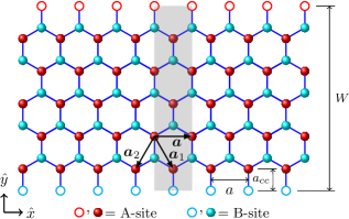
A zigzag graphene nanoribbon (ZGNR) is a strip of monolayer graphene CastroNetoReview2009 ; DasSarmaReview2011 that has been cut such that the edges along its length have a zigzag shape, as shown in Fig. 1. We take the ribbon to lie in the () plane, with as the longitudinal direction along which the ribbon extends over all space; then identifies the direction across the ribbon, along which the electron states are confined.
We assume passivated carbon atoms at the longitudinal boundaries, as if hydrogen atoms were adsorbed marconciniKDP ; Fujita_EELS_2015 ; this allows the passivation of any dangling edge states and the neutralization of the spin moments at the edges Fujita_EELS_2015 . We take as the effective width, where is the total number of atoms in the unit cell, is the graphene lattice constant, and is the carbon-carbon distance (see Fig. 1). The edge at is formed by A-atoms, while the edge at is formed by B-atoms. The lattice vector is and the atomic sites are set in terms of the graphene lattice vectors, and . The Dirac points of monolayer graphene are projected marconciniKDP into the one-dimensional Brillouin zone of the ZGNR, , as and .
We express the total wavefunctions as linear combinations of atomic orbitals that are centered at atomic sites A and B,
| (1) |
Then, following Marconcini and Macucci marconciniKDP , we employ the semi-empirical method to describe with a smooth envelope function approach. The coefficients and in Eq. (II.1) can be written as
| (2a) | ||||
| (2b) | ||||
where the are the envelope function components associated with the Dirac point and the orbital at atom A(B)111The graphene’s honeycomb lattice is composed by two distinct triangular lattices, A and B. On each sub-lattice all atoms are equivalent.. In writing Eq. (2) we have replaced for , on the basis of two assumptions. First, we assume that atomic orbitals are strongly localized at their corresponding atom, and second, we assume that the envelope functions are slow-varying functions of near the () Dirac point. These envelope functions satisfy the Dirac equation,
| (3) |
where , is the nearest-neighbor hopping parameter and is the graphene Fermi velocity. Because of the translational symmetry along , each envelope function can be factorized as the product of a propagating plane wave along the length direction (), and a function confined along the width direction (),
| (4) | |||||
| (5) |
where () is the wavevector along the length of the ribbon, measured from the Dirac point (). The passivation of the carbon atoms at the edges terminates the orbitals thereat, thus it is reasonable to assume that the full wavefunction vanishes at the lattice sites located at the effective edges. This leads to the following boundary conditions for the confined part of the envelope functions marconciniKDP ,
| (6a) | ||||||
| (6b) | ||||||
These boundary conditions and the block diagonal form of the matrix in Eq. (II.1) cause the envelope functions at to be uncoupled from their counterparts at ; therefore they can be studied separately. With the use of Eq. (4), the Dirac equation for the valley is
| (7) |
The solutions of Eq. (7) are of the form marconciniKDP ,
| (8) | ||||
| (9) |
where . Under the boundary conditions (Eq. (6a)), this leads to a relation between the transverse () and the longitudinal () wavenumbers,
| (10) |
which shows that they are coupled for ZGNR. If is taken to be real, then Eq. (10) reduces to
| (11) |
and without loss of generality we assume to be positive. Equation (11) supports two eigensolutions for , which we label as for positive energies and for negative energies; both correspond to states strongly confined at the edges, henceforth referred as edge states marconciniKDP ,
| (12) | |||||
| (13) | |||||
| (14) |
where is a normalization length along the direction. We have also set , and is the usual wavefunction normalization coefficient,
| (15) |
and the eigenenergy is
| (16) |
Conversely, if we consider solutions of Eq. (10) with purely imaginary, of the form with real, then Eq. (10) reduces to
| (17) |
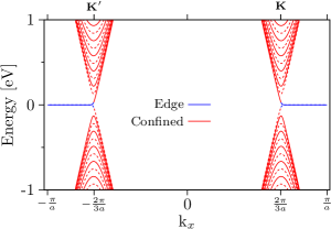
where, without loss of generality, we take to be positive. These solutions give states that extend over the full width of the ribbon, and are known simply as confined states; for these we set and label them by , starting with for those with energies closest to zero. These confined states exist for any real , except those with band index , which exist only for . The dispersion relations of the confined states with band index connect with that of the edge states; both share the band index (transition from the red to the blue traces in Fig. 3). The confined states have the form
| (18) | |||||
| (19) | |||||
| (20) |
where
| (21) | |||||
| (22) |
We can indicate any of the edge or confined states simply by , where if the state is confined, while if then the state is confined for , but it is an edge state if .
Equations (16) and (22) describe the bandstructure of ZGNR, shown in Figs. 2 and 3. The edge states are flattened towards the zero energy level for (Fig. 3), whereas the confined states have a parabolic structure around the Dirac points, with an axis of symmetry at , except for the two confined states nearest to zero energy, with band index and (Fig. 3). These confined states are associated with the Dirac cones of 2D graphene. Since the extrema of the confined states occur at , we can express the band energies at such value of as
| (23a) | ||||
| (23b) | ||||
for the edge and confined states, respectively. This indicates that the band gap scales as and provides an estimate of the photon energy at which the absorption edge occurs with respect to the ribbon width . It turns out that the sign functions appearing in the expressions for [Eq. (12) for edge states and Eq. (18) for confined states] alternate for consecutive states, being for the first state above zero energy, for the next up, and so on; the situation is reversed for negative energies. This sign factor plays an important role in the selection rules of the quantities we calculate. Therefore we indicate these sign factors on the bandstructure diagram [Figs. 2 and 3): a solid line indicates that the confined part of an A-site component of the envelope function has , whereas a dashed trace means it has .
II.2 Velocity matrix elements
We employ the envelope functions given by Eq. (4) in order to calculate the velocity matrix elements (VME) that describe the coupling between two states and as,
| (24) |
where is a wavenumber and , are band indices. The velocity operator is given by , which, together with the Hamiltonian in Eq. (7) for the valley,
| (25) |
leads to , where and are the Pauli matrices and is graphene’s Fermi velocity. The resulting expressions are given in Appendix A, Table 2, and obey the following selection rules:
| (26a) | |||
| (26b) | |||
We close this section by mentioning that the solutions corresponding to the Dirac point are analogous to those presented here for . As shown by Marconcini et al. marconciniKDP , the wavefunctions for the A sites, Eqs. (12) and (18), at the differ by a sign factor from those at . Moreover, the velocity operator at the has the form . This, together with the properties of the envelope functions at both valleys, causes the component of the VME at to have opposite sign of those at ; the components of the VME are the same near as near .
III Coherent injection and control
III.1 Framework
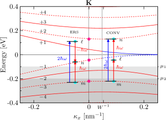
In this section, we describe the general framework of the two-color coherent control scheme. As mentioned in the Introduction, the quantum interference is between pathways associated with photon absorption processes arising from different phase related beams. These pathways connect the same initial and final states, as shown for the processes in Fig. 3, where we consider the two-color scheme with beams at and at . This figure depicts the two classes of processes we study in this paper.
The first, conventional processes, are those where current injection arises due to the interference of one-photon absorption (OPA) at and two-photon absorption (TPA) of (two) photons with energy ccontrolDrielSipe2001 ; this is depicted with the set of arrows on the right of Fig. 3, under the label “CONV”. In the remaining of the discussion, we label variables associated with conventional processes with a subindex ‘C’.
The second class of processes arise in experiments on narrow band gap or gapless materials, with , where is the energy band gap. Under this condition, current injection can arise due to the interference of OPA at and stimulated electronic Raman scattering (ERS) at RiouxERS . This ERS is indicated by the set of arrows at and in the left of Fig. 3, under the label “ERS”. We refer to variables associated with this Raman processes with a subindex ‘R’. We mention that in coherent control experiments on typical semiconductors, the beam frequencies employed are such that , and, consequently, the ERS current is absent because OPA at is impossible.
Following van Driel and Sipe ccontrolDrielSipe2001 ; ccontrolDrielSipe2005 , we calculate the one- and two-photon carrier injection and current injection rates due to the interaction with a classical electromagnetic field
| (27) |
in the long wavelength limit, where is the fundamental frequency. The interaction between the electric field and the electron system is accounted by the minimal coupling prescription in the Hamiltonian of Eq. (25); we do the usual replacement , for , with , and obtain the interaction Hamiltonian that acts as the perturbation,
| (28) |
where is the electron charge and is the vector potential associated with the electric field, . We treat this problem using standard time-dependent perturbation theory and Fermi’s golden rule. Since we are interested in OPA, TPA and ERS processes, the unitary evolution operator is expanded perturbatively up to second order,
| (29) |
where
| (30) |
and
| (31) |
Under the perturbation of Eq. (28), the evolution of the system’s state is not just the ground state , but it also contains an amplitude of the excited state (this ket corresponds to a state with an electron-hole pair),
| (32) |
where is the probability that the system is at ; the missing terms in Eq. (32) correspond to higher order excitations, which we neglect in this work. The carrier injection and the current injection rates are given by
| (33) | |||||
| (34) | |||||
respectively, where is the normalization length introduced below Eq. (14). To describe the optical processes we are interested, we compute up to second order (a tutorial derivation can be found in Ref. ccontrolDrielSipe2001 ; see also Ref. RiouxERS ). Then, the macroscopic expressions for these injection rates get the form,
| (35) | |||||
| (36) | |||||
| (37) | |||||
| (38) |
where repeated indexes indicate summation, is the fundamental frequency, and account for the first- and second-order absorption processes, respectively; overall refers to the rate of injected carriers per unit length along the ribbon (carriers per unit length per unit time). The OPA coefficient is described by a second-order tensor, , while the TPA and the ERS absorption coefficients are described by fourth-order tensors, and , respectively. Here, includes the electron and hole contributions to the current (charge per unit time), injected per unit time along the ribbon. The current injection coefficient in Eq. (38) includes the conventional and the ERS contributions, i.e., . In the following sections, we give the full expressions for these coefficients. Note that the coefficients can be chosen such that and .
III.2 First-order absorption process
We calculate the expressions for the coefficients and appearing in Eq. (35)–(38) using Fermi’s golden rule. For the one-photon absorption coefficient, we obtain
| (39) | |||||
where we have gone from a sum over states to an integral over reciprocal space by . In this expression the sum runs over all bands, filled and empty (similarly for the other response functions considered here); and is the energy difference between two states at a given . A factor of two has been included to account for spin degeneracy, which we do throughout the paper. The components of the VME at the and valleys differ just by a sign while the components of the VME are the same. Consequently, since all integrals over reciprocal space include pairs of VME, the integration over can be restricted to a single valley, , and another factor of two included to account for the contribution of the valley.
The occupation of the states is described by the Fermi-Dirac distribution. In all of our integrals over reciprocal space , with at temperature and chemical potential . Until the end of Sec. IV, we confine ourselves to zero temperature, hence , where is the Heaviside step function. Because of the selection rules for the VME, Eq. (26), the only nonzero components of the one-photon coefficient are and , which we plot in Fig. 4 for a system at zero chemical potential. As a comparison dropoff , we include plots of , where is the effective width of the ribbon,
| (40) |
and is the OPA coefficient for a 2D monolayer of grapheneRioux2011 ; here is the universal optical conductivity of graphene, and , are the spin and valley degeneracies, respectively. For ZGNR, the main difference between the two OPA coefficients is that diverges at zero photon energy, due to a divergence in the joint density of states (JDOS) between bands and . In contrast, for such a pair of bands is identically zero, due to the VME selection rules. For an undoped ZGNR, displays its first divergence at about 0.15 eV, which is the value of the band gap at zero Fermi level, and corresponds to the onset of the transitions and at ; these four states give the initiation energy for . In the following we indicate a transition from band to band by ; hence, for zero chemical potential and zero temperature, the possible transitions have and . In general, the and OPA coefficients possess an infinite number of divergences that arise due to the infinite number of parabolic bands in the bandstructure. Indeed, the JDOS between states with band index and ,
| (41) |
can be shown to diverge as for the confined states, and as for edge states, where is the photon energy and is the energy band gap between bands and . In frequency space, these divergences occur at photon energies such that ; in reciprocal space, they occur at points where argument of the delta function has a zero derivative. The absorption coefficients inherit these JDOS divergences if the associated velocity matrix elements are nonzero at the at which . The sensitivity of an experiment to these divergences would depend on the resolution of the photon energy and on the magnitude of the velocity matrix elements, as well as on the presence of scattering effects that are not included in this simple treatment. In every pertaining Figure, we signal the location of these JDOS divergences by small green ticks. An interesting characteristic of and is that the divergence at the initiation energy always involves an edge state (see Table 1); this is reasonable, as these states are involved in the minimum band gap for an undoped system.
As mentioned above, the sum over states runs over all bands, filled and empty, but for a given photon energy range (e.g. V, as in Fig. 4) the sum requires a finite number of bands. We refer to this as the “full” response. In order to highlight the contribution of the edge states, we also compute the response coefficients with a restricted sum over states , such that or are , e.g., ; we refer to this as the “edge” contribution and in the appropriate figures we plot it with black-dashed lines. This allows us to easily identify the contribution to OPA from states at bands . At low photon energies such contribution is dominant: for , all transitions at photon energies eV are from or to edge states; for , all transitions at photon energies eV are from or to edge states. Consequently, at low-photon energies the “full” and “edge” contributions are indistinguishable. This is shown in Fig. 4 (see also Table 1), where for comparison we also plot , where is the OPA coefficient of graphene calculated Rioux2011 at the same level of approximation adopted here; it is clear how the presence of the edge states in ZGNR significantly modifies the OPA. Finally, we mention that the Dirac delta functions appearing in all our expressions are treated with an interpolation scheme interpNote .
| Peak | ||||
| number | E (eV) | Transition | E (eV) | Transition |
| 1 | 0.149 | 0.000 | ||
| 2 | 0.323 | 0.236 | ||
| 3 | 0.350 | 0.410 | ||
| 4 | 0.498 | 0.439 | ||
| ⋮ | ⋮ | ⋮ | ⋮ | ⋮ |
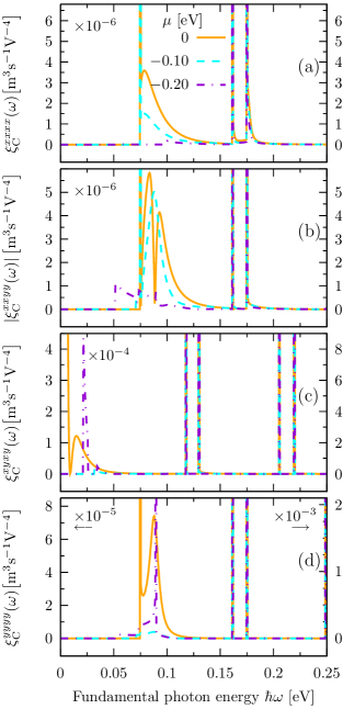
III.3 Second-order absorption processes
III.3.1 Conventional process
In this section, we start by considering the second order process related to the absorption of two photons of energy , indicated by the rightmost arrows in Fig. 3. Carrying the perturbation calculation up the second order, we obtain the two-photon absorption (TPA) coefficient,
| (42) | |||||
where
| (43) |
which we regard as the effective velocity matrix element (effective VME) for the second order conventional process (C) process. Here is a small constant introduced to broaden resonant processes (discussed below) and the sum over corresponds to the virtual electron and virtual hole contributions ccontrolDrielSipe2001 . Although this sum runs over all bands (filled and empty), a converged value is obtained for bands for a photon energy range of 0–1 V. From the selection rules for the regular VME, Eq. ((26)), we obtain the selection rules for ,
| (44a) | ||||
| (44b) | ||||
| (44c) | ||||
and from this we identify eight nonzero components, four of them independent, namely and , which we show in Fig. 5. A feature of these coefficients is that the onset of the two-photon absorption signal is at the minimum band gap between bands , except for , which has its onset at 0 eV; this follows from the selection rules for the effective VME, which are inherited from the usual VME, and indicate that the transition is allowed.
As we found for the OPA coefficients , the TPA coefficients suffer from divergences, but for the TPA coefficients they are of two types: JDOS divergences and effective-VME-divergences. The latter results when the nominal virtual state lies at the average of the energies between two transition states, and , i.e., when (see Eq. (43))
| (45) |
Such condition corresponds to a resonant TPA and an instance where this occurs is indicated on Fig. 3 by the three dots along the vertical line at . In Fig. 5 we distinguish these two types of divergences by small vertical lines of different color; a green tick indicates the presence of a JDOS-divergence, while a red tick indicates the presence of an effective-VME-divergence. In order to broaden the latter resonances, a small damping constant of 20 meV was introduced in the denominator of Eq. (43). This value, which is close to the thermal energy associated with room temperature, was chosen arbitrarily. A more detailed theory would be necessary to indicate how these resonances are really broadened; the choice we make here simply allows us to identify easily where these resonances occur in our calculations. We mention that the onset of is due to the transitions and , which are free from resonances because the matrix elements to the intermediate states (one of the edge bands that would lead to a divergent condition) are forbidden by the selection rules. Therefore, in the photon energy range 0 to 0.15 eV, the coefficient is free of resonances.
We present the coefficients in Fig. 5, and identify the edge contributions to them (black-dashed lines). As we found for , for the edge states make a dominant contribution at low photon energies, and are involved at the onset of TPA. As a comparison dropoff , in Fig. 5, we include plots of , where is the effective width of the ribbon,
| (46) |
and are the TPA coefficients for a 2D monolayer of graphene Rioux2011 ; as before, and are the spin and valley degeneracies, respectively.
III.3.2 ERS process
Now we consider another second order process involving light at and light at , stimulated electronic Raman scattering, which can be characterized as virtual absorption at followed by emission at ; see the left diagram in Fig. 3. This process exists in semiconductors when the fundamental photon energy is larger than the band gap, which is always the case for an undoped ZGNR, because the edge states provide a zero-gap system. Following an earlier treatment of graphene RiouxERS , we find the ERS carrier injection to be
| (47) | |||||
where the effective VME for the ERS process are
| (48) |
As in Eq. (43), is a small constant introduced to broaden resonant processes and the sum over runs over all bands (filled and empty), but a converged value is obtained for bands for a photon energy range of 0–1 V. The first term in the sum of Eq. (III.3.2) corresponds to photo-emission by an electron, and the second to photo-emission by a hole RiouxERS . Note that due to the different frequencies involved in Eq. (37), symmetrization of is unnecessary. The selection rules for are the same as those for (Eq. (44)); note, however, that , although and satisfy the same selection rule. From this we identify six nonzero terms for the ERS carrier injection coefficient, , , , , , and . As do the conventional coefficients, the ERS coefficients suffer from JDOS and effective-VME divergences, the later arising whenever
| (49a) | |||||
| (49b) | |||||
is satisfied. These conditions correspond to resonant processes, when a state is located at an energy above (below) the final (initial) state (). As in Eq. (43), a small damping constant of 20 meV was introduced in the denominators of Eq. (III.3.2). All of these ERS coefficients present a large number of these resonances, causing to be highly sensitive to the value of the parameter. However, these resonances are of small magnitude for the energy range chosen for Fig. 6, hence they are not apparent. As shown, three of these components have their onset at zero photon energy, because the symmetry properties of the involved matrix elements allow for transitions between the two edge states.
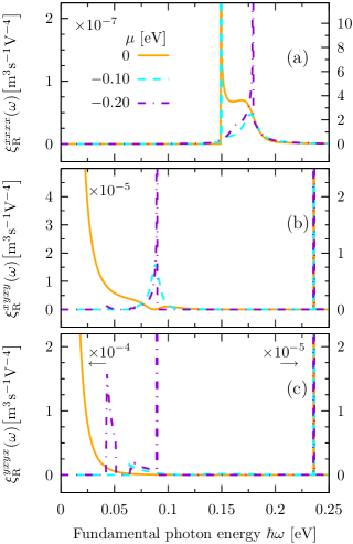
III.4 Current Injection
III.4.1 Injection coefficients
We begin with the expression for , the current injection coefficient characterizing the conventional process. Here the interference between the TPA at with OPA at (see the right diagram in Fig. 3) leads to net current injection coefficients (including electron and hole contributions) given by ccontrolDrielSipe2001
| (50) | |||||
From the selection rules for the regular and the effective VME, Eq. (26) and Eq. (44), we identify three nonzero current injection coefficients, and . Notice that for all these tensors the first Cartesian component is : Due to the confinement of the ribbons along the direction (see Fig. 1), the current injection can only flow along the direction, and all tensor components are zero.
Turning to the expression for , the current injection coefficient characterizing the interference between the ERS discussed above and the OPA at (see the left diagram in Fig. 3), including both electron and hole contributions we find
| (51) |
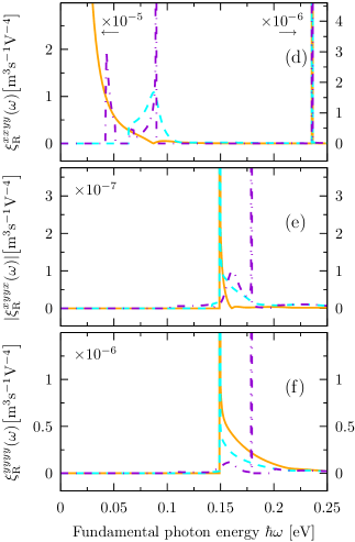
where is given by Eq. (III.3.2). On the basis of the matrix elements selection rules, we identify three nonzero ERS current injection coefficients, , , and .
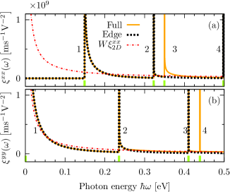
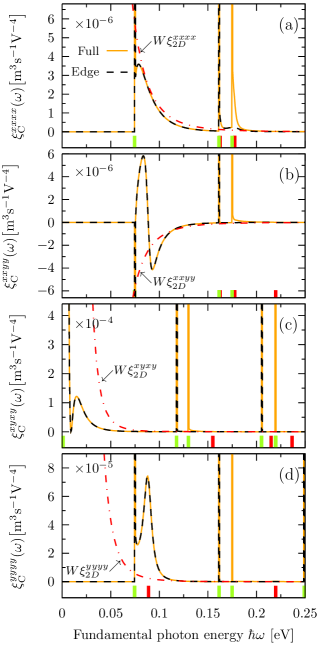
Over the frequency range shown in Fig. 7, the conventional and the ERS current injection coefficients are of the same order, dropping off as the inverse of the third power of the photon energy, as do the coefficients for graphene RiouxERS . Thus we only plot the total injection coefficients . For comparison, we include plots of (with the respective values of the Cartesian indices), where
| (52) |
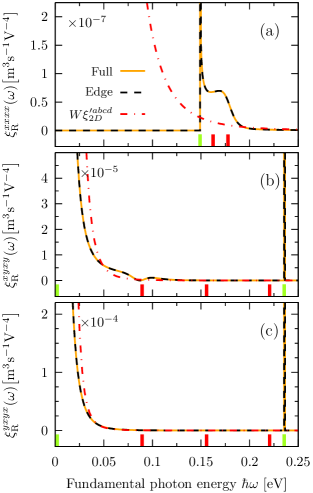
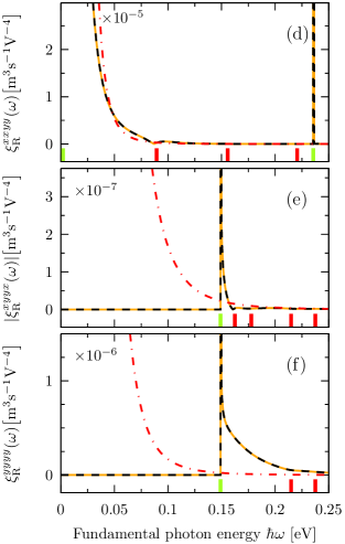
and are the net current injection coefficients for a 2D monolayer of grapheneRiouxERS ; as before, and are the spin and valley degeneracies, respectively. As we saw for carrier injection, the edge states provide the strongest contribution at the onset of current injection. Another characteristic of these coefficients is that has its onset at the band gap between bands , while and have their onset at 0 eV. This is due to the selection rules that the matrix elements involved in both the conventional and ERS process satisfy, allowing transitions between bands . An important characteristic of the current injection coefficients is that they are free of JDOS divergences, because the diagonal matrix elements in their respective expressions, Eqs. (50) and (51), are identically zero at the at which the minimum gap occurs. However, a number of effective VME resonances do exist at photon energies indicated by the small red ticks in Fig.7, such that Eq. (45) is satisfied. As explained before, the magnitude of these resonances is broadened by a small damping constant. These coefficients are shown in Fig. 7, where we present the net current injection arising from the addition of the conventional and ERS contributions, i.e., .
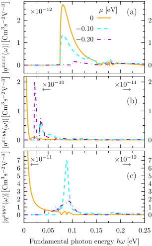
III.4.2 Swarm velocities
The numerical values of the coefficients , , and do not immediately give a sense of the average velocities with which the electrons and holes are injected. Sometimes an average, or swarm velocity is introduced to indicate this ccontrolDrielSipe2001 . In the system considered here, we could introduce a swarm velocity for both the conventional and ERS processes, according to
| (53) |
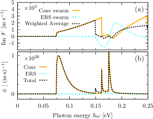
where for because arises from the interference of OPA at with TPA at , while for because arises from the interference of OPA at with the ERS described above. Besides describing an average speed that characterizes the injected carriers, one can consider maximizing Eq. (53) by using appropriate phases in the optical beams, and adjusting the relative amplitudes of the light at and . Considering just the swarm velocity of the conventional process, such optimization leads to equal OPA and TPA, and it follows that the intensity of the fundamental beam at should be about half an order of magnitude larger that of the beam at , for a fundamental photon energy of about V. In contrast, the swarm velocity of the ERS process depends only on the intensity of the beam at . Further, in trying to optimize the net swarm velocity, determined by the total current injected divided by the total carrier density injected, one finds that the beam at should have an intensity about an order of magnitude larger than the beam at . Since in typical experiments the beam at is obtained by second harmonic generation of part of the beam at , this would be impractical. Thus we calculate the conventional and Raman swarm velocities for typical sun-norris2010 beam intensities of the fundamental and second harmonic fields, shown in Fig. 8. We complement these carrier velocities with the total average velocity of the injected carriers
| (54) |
also evaluated at typical sun-norris2010 beam intensities. These carrier velocities are shown in Fig. 8. As a reference, at the photon energy of 0.25 eV, the maximum swarm velocity of the conventional process for a monolayer of graphene is ms-1. Hence the carrier velocities in ZGNR are comparable to those on a monolayer of graphene, as might be expected.
IV Doping
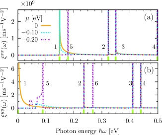
In the previous sections, we investigated the carrier and current injection at zero chemical potential. Since the dispersion relations of the edge states in ZGNR have a zero band gap and are flattened for (Fig. 3), those states are always involved at the onset energy of all of the optical response coefficients studied here. This suggests that doping is an effective method to alter the population of these two bands and the current that can be injected by the optical transitions between them. In this section, we revisit the calculations of , and for a negative chemical potential, corresponding to a -doped system. Besides the modified contribution from the edge states, we will also see significant modification in the contributions from other bands, particularly in the region near the and points, where doping leads to either a “valley” of filled states (-doped), or a “hill” of unfilled states (-doped); see Fig. 3.
We consider two negative Fermi levels, eV and eV, which in Fig. 3 we indicate by the upper boundaries of the grey areas. The value of eV is interesting because, at this chemical potential, the flat part of band (i.e., the region where , cf. Fig. 3) contains empty states; this condition allows transitions from lower energy bands with final states in band , but also disables transitions from band to upper bands. The second value, eV, is interesting because at this potential a “hill” of unfilled states arises in the first parabolic band (band in Fig. 3) at energies below our nominal value of zero.
We present the results of the calculations of OPA coefficients for
those values of the chemical potential in Fig. 9.
In an undoped sample, the JDOS divergences in at low photon
energies are due to the onset of the transitions
and (see Table 1
and Fig. 4). Since all of these transitions involve bands
, any nonzero chemical potential has the capacity to
significantly alter the OPA at these photon energies.
For instance, if the Fermi level is at eV, then the flat
part of band contains empty states, and the low
photon energy divergences are removed. In
addition, at this chemical potential transitions of the type
, for odd and are permitted.
However, the contributions to the OPA from these new
transitions are of smaller magnitude than the contribution from the
transition, which is unaffected by the eV doping. For
this reason, the transition remains as the main contribution
to the coefficient at low photon energies at this chemical
potential (see
Fig. 9).
At the Fermi level eV, the edge states are completely empty, as are the states at the higher points of band near the and points. This condition allows transitions of the type , for even and , and also forbids transitions of the type , for odd and , and near the and points. It is this latter restriction which significantly changes the coefficient near its onset. A further decrease in the Fermi level would consistently remove the divergences in at low photon energies. All these observations were confirmed with a band-by-band calculation of .
The effect of doping the system has a larger influence on the onset energy of that on that of . This is because the JDOS divergences at low photon energies relevant for are due to the transitions , and (cf. Table 1). Therefore, even for small doping, the large contribution coming from the transitions between the two edge states (bands , ) is significantly decreased, and leads to a greater change of the magnitude of than of the magnitude of . A special signature of for V (dark-violet signal, Fig. 9 b)) is the presence of two narrow peaks at 0.045 and 0.075 eV; the first of these peaks is due to the transition, while the second is from the transition. These two transitions are active only for those states at which the “hill” of band is empty (see Fig. 3). Notably, the transition brings a new JDOS divergence because it is active over a range of reciprocal space that includes , where both bands have their maximum and their energy difference has a zero derivative (see the discussion below Eq. (41)).
In general, all these new transitions involve more JDOS divergences if the range of over which they are active includes the at which the band pairs have their maxima or minima. For instance, the divergences 1–4 in Fig. 9 are the same as those in Fig. 4 and Table 1, but the divergences 5–6 arise due to the new transitions allowed at nonzero chemical potentials: in Fig. 9 a), at the chemical potential V, the divergence 5 at eV is due to the transition , which is active over a range of that includes the at which bands have their maxima, hence a new JDOS divergence appears. Likewise for in Fig. 9 b) at V: divergences 5 at eV and 6 at eV exist because the transitions and are active over regions of reciprocal space that include the at which such bands have their maxima.
In Fig. 10, 11, and 12 we present the nonzero , , and coefficients for selected nonzero Fermi levels. As was seen for , doping the ZGNR has the effect of modifying the responses around their onset energy, either due to the removal of some transitions, or due to the appearance of new ones, which in the undoped system were forbidden because the initial and final states were filled [e.g. () or ()]. This shows that doping is an effective way of modifying the carrier and current injection in ZGNR, where the most significant changes are due to the removal of density of states at the edge bands.
We close this section by mentioning that we performed finite temperature calculations at room temperature; this was achieved by implementing a temperature dependence of the Fermi factors through the Fermi-Dirac distribution. We found that the only significant change is in that the onset energy of the coefficients , , and are smaller. However, the magnitudes of the coefficients at energies near the lower onsets are several orders of magnitude smaller that the magnitudes of the corresponding coefficients at zero temperature near their energy onsets.
V Limits of the model
The model employed in this work inherits the limits of applicability of time-dependent perturbation theory, which is restricted to situations of low electron-hole pair densities haug04 (for high injection densities a density matrix formalism could be employed to study the dynamics). The regime of validity of the perturbation treatment used here can be estimated: we require the populated fraction of excited states accessible to a typical Gaussian pulse to be small.
V.1 Graphene sheet
As a reference, we first consider monolayer graphene. When the electric fields of the optical beams are all aligned along , the one- and two-photon injection coefficients for a 2D graphene sheet are Rioux2011 given by Eqs. (40) and (46). For each of and , we set the number of carriers injected per unit area to be less than the number of states per unit area accessible to the optical beam. Then taking the beam intensity as , we arrive to
| (55) | |||||
| (56) |
where is the time-bandwidth product for the optical beam (which we take as 0.44, typical for a Gaussian beam), is the pulse-duration, and m/s is graphene’s Fermi velocity.
V.2 Zigzag nanoribbons
The estimate for the nanoribbon case is similar to the graphene sheet, aside from the fact that the areal ratios become length ratios, i.e. for each one of OPA and TPA coefficients we set the number of carriers injected per unit length to be less than the number of states per unit length accessible to the optical beam, giving us
| (57) | |||||
| (58) |
where and where defined previously, is the velocity of the injected electrons in the conduction band, given by the matrix element , and is the velocity of the holes injected in the valence band, given by . Equation (58) provides the expression for the conventional () and ERS processes ().
In order to compare the limiting intensities of our model for a graphene sheet and for ZGNR, we assume a typical pulse duration of fs and beam wavelengths of and for the and beamssun-norris2010 . Then we identify the states that contribute at these two wavelengths, and find that, on average, . From Eqs. (55) and (57), at m,
| (59) |
and from Eqs. (56) and (58), at m,
| (60) |
Equations (59) and (60) indicate that the limiting intensities of our model are similar for a graphene sheet and for a ZGNR, within an order of magnitude.
We find that, under the assumptions made in this section, the estimated limit for the beam intensities at in the ZGNR and the 2D graphene are about two orders of magnitude below the intensities used in some experiments sun-norris2010 on 2D graphene, where coherent current injection was observed. Due to relaxation processes, of course, the number of allowed carrier excitations below saturation is expected to be higher than our estimates, leading to larger values of the beam intensities for which a perturbation approach would be valid. Based on the estimates in Eqs. (59) and (60), if relaxation processes affect the ribbon samples as effectively as they do for 2D samples, we can expect coherent control in ZGNR to be observable at the higher intensities used in 2D graphene experiments.
VI Summary and Discussion
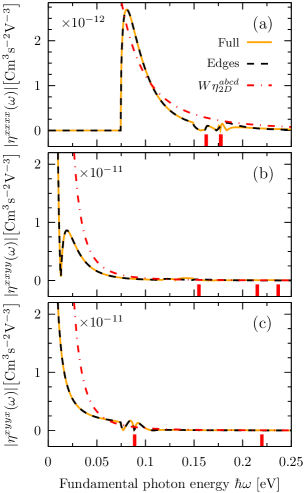
We have calculated the response coefficients for one- and two-photon charge injection and the two-color current injection in a graphene zigzag nanoribbon; we use the semi-empirical method to describe the electron wavefunctions by smooth envelope functions.
The only nonzero one-photon injection coefficients correspond to the case of all- or all- aligned fields, i.e., and . These two coefficients possess a rich structure of divergences, caused by divergences of the joint-density-of-states originating from the infinite set of parabolic bands present in the zigzag nanoribbon. These two coefficients have distinct selection rules for the allowed transitions.
The two-photon carrier injection coefficients drop off as the fifth power of the photon energy at large photon energies, as they do for monolayer graphene. Moreover, these coefficients possess two classes of divergencies. One corresponds to the joint-density-of-states divergences associated with the parabolic bands. The second class corresponds to divergences arising from resonant conditions, when the two-photon absorption processes arise from sequential one-photon absorption processes between real states. In our calculation here we broadened these resonances phenomenologically, but a more sophisticated treatment of these resonantly enhanced transitions is an outstanding problem on which we hope this work will encourage further study. The onset of the signals is determined by the minimum energy band gap and the selection rules for these coefficients.
We calculated the electron and hole contributions to the conventional and the stimulated electronic Raman scattering (ERS) current injection processes, finding that the only nonzero components are associated with current injected along the length of the nanoribbon, as expected. The behavior of these coefficients as a function of the photon energy follows the behavior of 2D graphene [] at large photon energies, aside of the resonances present in the ribbons. We have also calculated the so-called swarm velocity of the injected electrons, which inherits a rich structure as a function of the photon energy due to the details of the structure of the injection coefficients. All these calculations were presented for a system at zero Fermi level and zero temperature. However, we also carried finite temperature calculations and found that, within this model, finite temperatures only account for changes at the onset of the signals, which are several orders of magnitude smaller than the nominal values at zero temperature.
Lower bound estimates on the permissible incident intensities for which the calculations here can be valid were presented. They are similar to those of monolayer graphene, where coherent current injection has been observed at much higher intensities than these simple estimates, which do not take into account the relaxation effects in the excited populations. Thus experiments to demonstrate coherent current injection in ZGNR seem to us to be in order.
For experiments contemplated for ribbons of different width than those studied here, it is important to note that simple scaling arguments show that the wider the ribbon, the stronger the confinement of the energy bands. As shown in this work, at low photon energies, the band gap follows a linear relation with respect to the inverse of the ribbon width. Consequently, increasing the width of the ribbon decreases the energy band gap between any pair of bands. This in turn shifts the onset energy of the response coefficients towards zero energy and increases the number of JDOS divergences per photon energy. For instance, the onset of the response coefficients when light is polarized along the length of the ribbon is determined by the bangap between bands (see Fig. 3). For such pair of bands, a linear fit shows that the band gap depends on the ribbon width as with . Besides altering the onset energy of the responses, a larger width also leads to a larger magnitude of the injection coefficients, larger than would be expected simply on the basis of the increase in material; e.g., a width increase of about doubles the size of .
As the outstanding signature of the zigzag nanoribbons are the strongly localized edge states, we have identified their contribution to the carrier- and current-injection processes. In all cases the edge states always participate in the onset of the signals. This lead us to consider a second scenario to study these localized states: given that the dispersion relations of these states are flattened towards zero energy for certain regions in -space, we re-visited our calculations considering doped scenarios. We found that that even small doping levels allow for significant changes around the onset energy of the signals. This is because the large joint-density of states present between the edge states is diminished with nonzero chemical potentials. Due to the relative ease of doping graphene systems, the present work shows that zigzag nanoribbons offer an excellent opportunity to investigate scenarios in which electrical currents can be generated and controlled optically. While more sophisticated treatments of the electron states and the inclusion of electron-electron interaction Yang_Cohen_Louie_2008 ; lado2015 will undoubtedly add to the richness of the injection processes, we hope that the description given here will motivate all-optical current injection experiments. Although coherent control has been studied and observed on graphene sheets, zigzag graphene nanoribbons have the advantage of having optical responses that depend strongly on the geometry and width of the ribbon. Moreover, as shown in the literature, the localized states present in these ribbons are highly sensitive to external fields, doping and functionalization. All these characteristics endow graphene zigzag ribbons with a richness absent in simpler graphene sheets.
VII Acknowledgments
C.S. acknowledges partial support from CONACYT (Mexico) and Rodrigo A. Muniz for useful discussions. J.L.C. acknowledges the support from EU-FET grant GRAPHENICS (618086), the ERC-FP7/2007-2013 grant 336940, and the FWO-Vlaanderen project G.A002.13N. J.E.S. and C.S. acknowledge support from the Natural Sciences and Engineering Research Council of Canada (NSERC). All the authors acknowledge A. Paramekanti and M. Killi for drawing our attention to this problem.
Appendix A Velocity matrix elements
| Type | Expression | Conditions |
|---|---|---|
| nConf | , or | |
| , or | ||
| mConf | ||
| nEdge | ||
| mEdge | ||
| nConf | ||
| mEdge | ||
| nEdge | ||
| mConf |
References
- [1] T.Ogawa and Y.Kanemitsu. Optical Properties of Low–Dimensional Materials. World Scientific, 1996.
- [2] Kyoko Nakada, Mitsutaka Fujita, Gene Dresselhaus, and Mildred S. Dresselhaus. Edge state in graphene ribbons: Nanometer size effect and edge shape dependence. Phys. Rev. B, 54:17954–17961, Dec 1996.
- [3] L. Brey and H. A. Fertig. Electronic states of graphene nanoribbons studied with the Dirac equation. Phys. Rev. B, 73:235411, Jun 2006.
- [4] P. Marconcini and M. Macucci. The method and its application to graphene, carbon nanotubes and graphene nanoribbons: the Dirac equation. La Rivista del Nuovo Cimento, pages 489–584, 2011.
- [5] Hoonkyung Lee, Marvin L. Cohen, and Steven G. Louie. Selective functionalization of halogens on zigzag graphene nanoribbons: A route to the separation of zigzag graphene nanoribbons. Applied Physics Letters, 97(23):233101–1, 2010.
- [6] Gomes da Rocha, Clayborne, Koskinen, and Hakkinen. Optical and electronic properties of graphene nanoribbons upon adsorption of ligand-protected aluminum clusters. Phys. Chem. Chem. Phys., 16:3558–3565, 2014.
- [7] Li Yang, Marvin L. Cohen, and Steven G. Louie. Magnetic edge-state excitons in zigzag graphene nanoribbons. Phys. Rev. Lett., 101:186401, Oct 2008.
- [8] Jens Kunstmann, Cem Özdoğan, Alexander Quandt, and Holger Fehske. Stability of edge states and edge magnetism in graphene nanoribbons. Phys. Rev. B, 83:045414, Jan 2011.
- [9] M. Bellec, U. Kuhl, G. Montambaux, and F. Mortessagne. Manipulation of edge states in microwave artificial graphene. New J. Phys., 16:113023, 2014.
- [10] P. Delplace, D. Ullmo, and G. Montambaux. Zak phase and the existence of edge states in graphene. Phys. Rev. B, 84:195452, Nov 2011.
- [11] Oleg V. Yazyev. A guide to the design of electronic properties of graphene nanoribbons. Accounts of Chemical Research, 46(10):2319–2328, 2013. PMID: 23282074.
- [12] J M Luck and Y Avishai. Unusual electronic properties of clean and disordered zigzag graphene nanoribbons. Journal of Physics: Condensed Matter, 27(2):025301, 2015.
- [13] N Fujita, P J Hasnip, M I J Probert, and J Yuan. Theoretical study of core-loss electron energy-loss spectroscopy at graphene nanoribbon edges. Journal of Physics: Condensed Matter, 27(30):305301, 2015.
- [14] Marta Pelc, Eric Suárez Morell, Luis Brey, and Leonor Chico. Electronic conductance of twisted bilayer nanoribbon flakes. The Journal of Physical Chemistry C, 119(18):10076–10084, 2015.
- [15] D. Gosálbez-Martínez, D. Soriano, J.J. Palacios, and J. Fernández-Rossier. Spin-filtered edge states in graphene. Solid State Communications, 152(15):1469 – 1476, 2012. Exploring Graphene, Recent Research Advances.
- [16] Thomas Stegmann and Axel Lorke. Edge magnetotransport in graphene: A combined analytical and numerical study. Annalen der Physik, 527(9-10):723–736, 2015.
- [17] J.L. Lado, N. García-Martínez, and J. Fernández-Rossier. Edge states in graphene-like systems. Synthetic Metals, 210, Part A:56 – 67, 2015. Reviews of Current Advances in Graphene Science and Technology.
- [18] Han Hsu and L. E. Reichl. Selection rule for the optical absorption of graphene nanoribbons. Phys. Rev. B, 76:045418, Jul 2007.
- [19] Ken-ichi Sasaki, Keiko Kato, Yasuhiro Tokura, Katsuya Oguri, and Tetsuomi Sogawa. Theory of optical transitions in graphene nanoribbons. Phys. Rev. B, 84:085458, Aug 2011.
- [20] Takahiro Yamamoto, Tomoyuki Noguchi, and Kazuyuki Watanabe. Edge-state signature in optical absorption of nanographenes: Tight-binding method and time-dependent density functional theory calculations. Phys. Rev. B, 74:121409, Sep 2006.
- [21] M. Berahman, M. Asad, M. Sanaee, and M.H. Sheikhi. Optical properties of chiral graphene nanoribbons: a first principle study. Optical and Quantum Electronics, 47(10):3289–3300, 2015.
- [22] Wen-Huan Zhu, Guo-Hui Ding, and Bing Dong. The enhanced optical conductivity for zigzag-edge graphene nanoribbons with applied gate voltage. Applied Physics Letters, 100(10):103101–1, 2012.
- [23] Deborah Prezzi, Daniele Varsano, Alice Ruini, Andrea Marini, and Elisa Molinari. Optical properties of graphene nanoribbons: The role of many-body effects. Phys. Rev. B, 77:041404, Jan 2008.
- [24] E.A. Manykin and A.M. Afanas’ev. On one possibility of making a medium transparent by multiquantum resonance. J.Exptl. Theor. Phys., 25(2):828–830, November 1967. Original in Russian: ZhETF 52, No. 5, p. 1246-1249 (1967).
- [25] E.A. Manykin. Quantum interference and coherent control. Laser Phys., 11:60, 2001.
- [26] H.M. van Driel and J.E. Sipe. Ultrafast Phenomena in Semiconductors, chapter 5: Coherent Control of Photocurrents in Semiconductors, pages 261–306. Springer, 2001.
- [27] Dong Sun, Charles Divin, Julien Rioux, John E. Sipe, Claire Berger, Walt A. de Heer, Phillip N. First, and Theodore B. Norris. Coherent control of ballistic photocurrents in multilayer epitaxial graphene using quantum interference. Nano Letters, 10(4):1293–1296, 2010. PMID: 20210362.
- [28] J. Rioux, Guido Burkard, and J. E. Sipe. Current injection by coherent one- and two-photon excitation in graphene and its bilayer. Phys. Rev. B, 83:195406, May 2011.
- [29] Benjamin M Fregoso and Sinisa Coh. Intrinsic surface dipole in topological insulators. Journal of Physics: Condensed Matter, 27(42):422001, 2015.
- [30] Kiran M. Rao and J. E. Sipe. Coherent photocurrent control in graphene in a magnetic field. Phys. Rev. B, 86:115427, Sep 2012.
- [31] Rodrigo A. Muniz and J. E. Sipe. Coherent control of optical injection of spin and currents in topological insulators. Phys. Rev. B, 89:205113, May 2014.
- [32] Rodrigo A. Muniz and J. E. Sipe. All-optical injection of charge, spin, and valley currents in monolayer transition-metal dichalcogenides. Phys. Rev. B, 91:085404, Feb 2015.
- [33] A. H. Castro Neto, F. Guinea, N. M. R. Peres, K. S. Novoselov, and A. K. Geim. The electronic properties of graphene. Rev. Mod. Phys., 81:109–162, Jan 2009.
- [34] S. Das Sarma, Shaffique Adam, E. H. Hwang, and Enrico Rossi. Electronic transport in two-dimensional graphene. Rev. Mod. Phys., 83:407–470, May 2011.
- [35] The graphene’s honeycomb lattice is composed by two distinct triangular lattices, A and B. On each sub-lattice all atoms are equivalent.
- [36] J. Rioux, J. E. Sipe, and Guido Burkard. Interference of stimulated electronic raman scattering and linear absorption in coherent control. Phys. Rev. B, 90:115424, Sep 2014.
- [37] H.M. van Driel and J.E. Sipe. Coherent control: Applications in semiconductors. In Robert D. Guenther, editor, Encyclopedia of Modern Optics, pages 137–143. Elsevier, Oxford, 2005.
- [38] At large photon energies, the two-photon absorption coefficients for zigzag nanoribbons drop off with the fifth power of the photon energy, as they do for a monolayer of graphene.
-
[39]
We handle Dirac delta integrals of the form by doing an interpolation of the
integrand, such that
, where is the interpolated -point that satisfies the Dirac delta, , and is the unit step function. This interpolation scheme requires convergence on a single parameter, the number of points. More simple numerical treatments of the Dirac delta integrals with broadening functions (Lorentzian or Gaussian functions) require a larger number of -points to reach convergence. - [40] Hartmut Haug and Stephan W. Koch. Quantum Theory of the Optical and Electronic Properties of Semiconductors. World Scientific Publishing Company, 4 edition, 2004.