Multilayered cuprate superconductor Ba2Ca5Cu6O12(O1-x,Fx)2 studied by temperature-dependent scanning tunneling microscopy and spectroscopy
Abstract
Scanning tunneling microscopy/spectroscopy (STM/STS) measurements were carried out on a multi-layered cuprate superconductor Ba2Ca5Cu6O12(O1-x,Fx)2. STM topography revealed random spot structures with the characteristic length nm. The conductance spectra show the coexistence of smaller gaps and large gaps (pseudogaps) . The pseudogap-related features in the superconducting state were traced with the spatial resolution of 0.07 nm. Here, and are the tunnel current and bias voltage, respectively. The temperature, , dependence of follows the reduced Bardeen-Cooper-Schrieffer (BCS) dependence. The hallmark ratio 2 equals to 4.9, which is smaller than those of other cuprate superconductors. Here, is the superconducting critical temperature and is the Boltzmann constant. The larger gap survives in the normal state and even increases with above . The dependences of the spatial distributions for both relevant gaps ( map), as well as for each gap separately ( and ) were obtained. From the histogram of map, the averaged gap values were found to be meV and meV. The smaller gap shows a spatially homogeneous distribution while the larger gap is quite inhomogeneous, indicating that rather homogeneous superconductivity coexists with the patchy distributed pseudogap. The spatial variation length of correlates with the scale of the topography spot structures, being approximately 0.4 nm. This value is considerably smaller than the coherence length of this class of superconductors, suggesting that is strongly affected by the disorder of the apical O/F.
pacs:
68.37.Ef; 74.25.Jb.; 74.72.HsI Introduction
Despite the recent discoveries of new classes of superconductorsklemm12:book ; hirsch15:1 with high critical-temperatures (’s), including, e.g., magnesium diboride MgB2nagamatsu , iron superconductorskamihara ; hosono15 , carbon-based materialskubozono16 , H2S under high pressuresdrozdov15 , etc., the copper-oxide superconductors found in 1986 bednorz still remain the main object of the theoretical and experimental researchkeimer15:179 ; kordyuk15:417 . It can be explained by the highest achieved ’s at the ambient pressures and various unusual fascinating properties both from the scientific and technological points of view. However, even those numerous studies could not uncover the mechanism of superconductivity in cuprates as well as the origin of their high ’skresin09:481 ; kamimura12:677 ; mukuda12:011008 ; hashimoto14:483 ; das14:151 . Nevertheless, the energy gap structures, especially, the so-called pseudogap (PG) featureshufner08:062501 ; kordyuk15:417 ; yoshida16:014513 provide the community with the inestimable information, which helps to examine both the strength of the Cooper-pairing interactionhashimoto14:483 and the symmetry of the superconducting order parameterklemm05:801 ; kirtley11:436 . The quasiparticle energy spectra can also reveal the competing orderings strongly affecting the superconductivity in high- oxideslee06:17 ; hashimoto14:483 ; kordyuk15:417 ; tajima16:094001 . The magnitudes of the observed energy gaps in cuprates are of the order of several tens mV, that is very large as compared to their ’s if the Bardeen-Cooper-Schrieffer (BCS) relationships for the -wavebardeen57:1175 or -wavewon94:1397 pairings are taken as the reference values. Furthermore, it has been widely reported that these gap magnitudes were inhomogeneously distributed with the spatial scales of several nm in Bi-basedhowald ; kmlang ; matsuda1 ; mcelroy ; sugimotoPRB2006 ; machida ; fischer07:353 ; boyer2201 ; zeljkovic high- oxides. It is remarkable that the gap-value histograms are predominately double-peaked, which seems to be the manifestation of the superconducting gap and pseudogap intertwininggabovich16:1103 . Hence, the analysis of the varying inhomogeneities may be useful to understand the cuprate superconductivity because the observed gap spatial distributions include regions of the nanometer scale with gaps being so large, that the corresponding ’s found on the basis of the BCS relationships substantially exceed the actual ones. The origin of the inhomogeneities is not known for sure, although recent observations of Bi-based high- superconductors showed that they were closely related to the disorder in the interstitial oxygen and vacancy positions outside the CuO2 conducting layers, the defects acting as the scattering centerszeljkovic . One should not also rule out the possibility that the bizarre patterns of the spatial disorder is the consequence of the intrinsic phase separation extensively studied theoretically and most probably revealed experimentally in some of the objects concernedphillips03:2111 ; damascelli03:473 ; lee06:17 ; fischer07:353 ; vojta09:699 ; armitage10:2421 . However, some problems still remain unclear: (i) whether the inhomogeneous gap distributions are common to all high oxides and (ii) are they driven by the scatter of the Cooper pairing strength or the intensity of the competing interaction leading to the pseudogap formation? The answers to those questions can be obtained by extending the scope of tunnel measurements to other cuprates.
Recently, the high-quality single crystals of the multilayered cuprates with apical fluorine, Ba2Can-1CunO2n(O1-x, Fx)2 [F02(-1), is number of CuO2 planes] have been successfully synthesized iyo2001 ; iyo2003 ; shirage . Those compounds seem to be very promising because their exceeds 100 K. It is also very convenient, that the clean flat surface of BaO/F layer can be obtained by cleaving the single crystal. Hence, those compounds constitute a class of appropriate materials to investigate their surface nanoscale inhomogeneity depending on their superconducting properties. One can expect that they may serve as another testing ground to manifest gap-spread phenomena revealed earlier in the Bi-based cuprates. The superconducting properties of Ba2Can-1CunO2n(O1-x, Fx)2 can be controlled by changing the number of CuO2 planes , as shown in Fig. 1 (a). At first, increases with the sheet number , reaches its maximum at =3 and saturates at large mukuda12:011008 . It was also shown that the indicated dependence correlates with the charge carrier concentration profiles. (The non-monotonic dependence of on the charge carrier density is inherent, e.g., to the conventional BCS-Eliashberg theory of superconductivity, the decrease at high concentrations being the consequence of the strong electron-phonon-attraction screening in this limitgabovich78:1115 ; kresin90:1203 .) Specifically, according to the Nuclear Magnetic Resonance (NMR) experiments, each CuO2 plane demonstrates a different carrier concentrations, i.e., the inner CuO2 planes have lower carrier density than that of outer CuO2 planes. shimizuNMR_PRL2007 ; mukuda12:011008 . The NMR measurements also showed that the inner CuO2 planes tend to become antiferromagnetic while the outer CuO2 ones remain superconducting. In view of this complexity, it is no wonder that previous point-contact tunnel spectroscopy experiments in F0234 displayed multiple-gap structures, that were attributed to the superconducting gap and pseudogap miyakawaPCF0234 . In particular, the pseudogap features were suggested to be induced by the antiferromagnetic state developed in the inner planes below a corresponding critical temperature. Moreover, the angle resolved photoemission spectroscopy (ARPES) measurements of F0234 revealed double Fermi surfaces chenARPES , which the authors considered to originate from the two different types of planes, i.e. inner and outer ones. Thus, the multiple Fermi surfaces and the multiple gap structures are probably related to the coexisting antiferromagnetism and superconductivity in those multilayer materials. However, while the differences between the average carrier concentrations in the CuO2 layers were studied in sufficient detail by various means, the existence of intrinsic nanoscale inhomogeneities inside each CuO2 plane is still not understood.
Recently, we carried out Scanning Tunneling Microscopy (STM) experiments on F0256, which identified the apical O and F positions in the BaO/F layers by observing the spot structures sugimotoPhysC_ISS2008 ; sugimotoPhysC_ISS2010 . The inevitable disorder induced by substitutions of the apical O by F (anion replacement) should potentially affects the spatial energy gap distributions. Therefore, it is natural to expect that the inhomogeneous gap structures in F02(-1) would be observed in the precise STM/Scanning Tunnel Spectroscopy (STS) experiments, and the latter would clarify whether the nanoscale inhomogeneity is the common property of different cuprate superconductors.
In this paper, we present the corresponding systematic observations by the STM/STS technique of temperature ()-dependent gap distributions for the superconductors Ba2Ca5Cu6O12 (O1-x, Fx)2 with six CuO2 layers (F0256, shown in the scheme of Fig. 1(a)). The results confirmed that the multiple-gap structures with the spatially inhomogeneous magnitude distributions are indeed strongly affected by the disorder at the apical O/F location.
II Experimental
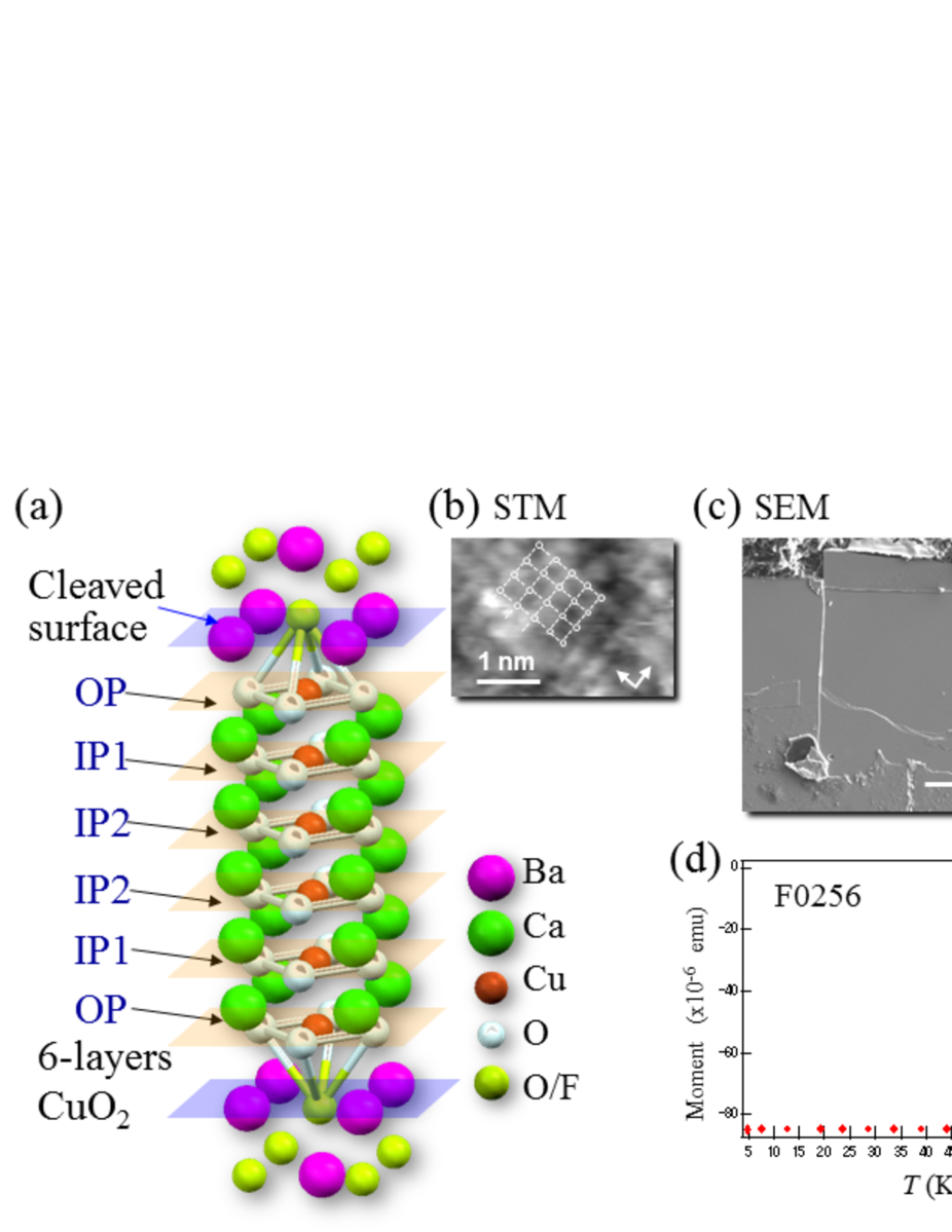
The single crystals of superconducting Ba2Ca5Cu6O12(O1-xFx)2 (F0256, 0.79) were fabricated by a high-pressure synthesis technique iyo2001 ; iyo2003 . The typical size of the single crystal is about 0.6 mm 0.6 mm 0.1 mm. The large-size single crystal of this composition is relatively easier to obtain than those of other compositions. Figures 1(b) and (c) show the examples of the STM image sugimotoPhysC_ISS2008 and the scanning electron microscope (SEM) image of the single crystal F0256 cleaved surface, respectively. A rather smooth surface is found by the SEM observation [Fig. 1(c)], which is suitable for STM measurements. The STM image [Fig. 1(b)] shows atomic arrangements with the spatial period of 0.38 nm (indicated by dashed lines). These structures should be attributed to the oxygen sites on the CuO2 sheet and Ba/F sites (indicated by circles), the result being basically similar to that obtained earlier for F0245 sugimotoPhysC_ISS2010 . We note that such atomic arrangements are observed only inside the area between the large spot structures [shown in Fig. 2 (a)]. The value of 70 K was determined by measuring the dependence of the magnetic susceptibility as shown in Fig. 1(d). The dependence of resistivity confirms this result. The x-ray diffraction (XRD) and electron probe micro-analysis (EPMA) measurements confirmed the adopted six-layered CuO2 phase indicated as the schematic model in Fig. 1(a). The composition ratio determined by EPMA revealed that the average Ba:Ca:Cu:F ratio was 2.00:5.13:5.78:1.59, which is in a good agreement with the ideal stoichiometric ratio for this compound.
The STM equipment used in this experiment is commercially based system (Omicron LT-STM) with upgraded modifications ekino2007JPCS ; sugimotoLBH . The single crystals were cleaved at 77 K under the ultra-high vacuum atmosphere of Pa. The exposed surface is considered to be the BaO/F layer as shown in Fig. 1(a). The Pt/Ir tip was cleaned by the high-voltage field emission process with the Au single crystal target just prior to the measurements. The STM/STS observations were carried out in the temperature range of 4.9 K to 290 K using the heating system in the ultra-high vacuum of Pa. Before STM/STS observations, the local barrier height (LBH; work-function) was measured on the basis of the relationship between the tunneling current () and the tip-sample distance () ( method sugimotoLBH ). Fig. 1(e) shows the simultaneously obtained LBH map of F0256 surface with 5 nm 5 nm measurement area. The histogram of LBH data extracted from the map are presented in Fig. 1(f), demonstrating sufficiently large values (3 eV) to carry out measurements in the tunneling regime. curves were obtained by numerical differentiation of the measured characteristics with the spatial interval of 0.07 nm. The voltage at the sample is considered as a reference one.
III Results and discussion
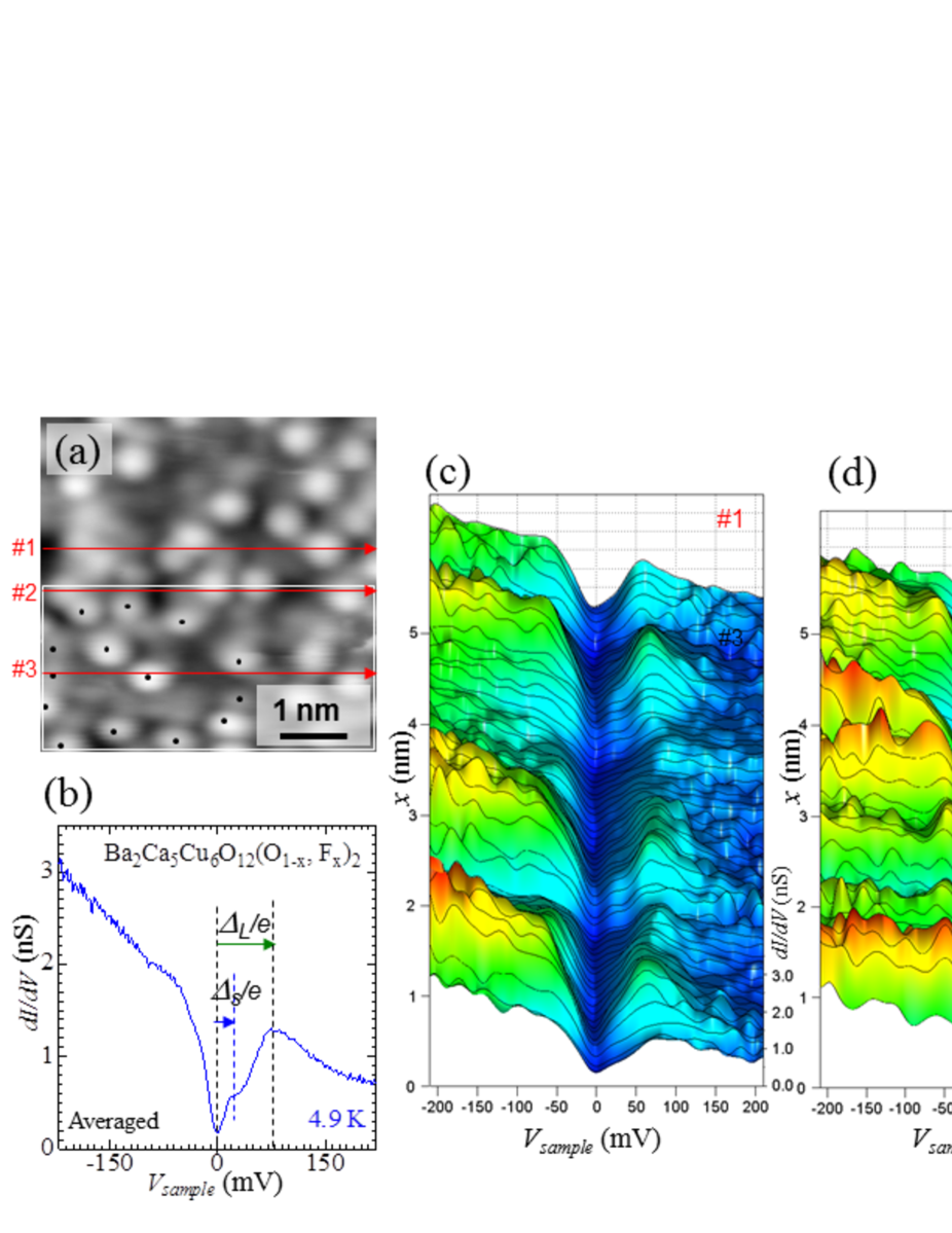
Figure 2(a) demonstrates an STM image (topography) of the cleaved F0256 single crystal surface at K for V and nA. The randomly distributed bright spots (indicated by black dots) of the sub-nanometer size are clearly observed over the whole scanned area. Such large spot structures have been already reported in our previous communications sugimotoPhysC_ISS2008 ; sugimotoPhysC_M2S ; sugimotoPhysProc_ISS2013 . These spots were suggested to correspond to the non-replaced apical oxygen of topmost BaO/F layers. This conclusions stems from the observation that the fraction of such spots in the STM images correlates with the O/F ratio obtained by the element analysis. Indeed, the spot density obtained by the direct counting was about 28% of apical O/F atomic sites, being in the fairly good agreement with the atomic ratio of apical O % found by the EPMA element analysis sugimotoPhysC_ISS2008 . It should be noted that clear periodic atomic structures were not visible in this frame. However, we observed the atomic corrugations with the period of 0.38 nm inside the interval between the spot structures, as is shown in Fig. 1(b). Additionally, our previous study of the other compound F0245 showed the existence of apparent atomic-lattice structures with such spots and the fourfold cross shaped clusters of the spotssugimotoPhysC_ISS2010 . Empirically from our experiments, such random spot structures were sometimes observed on contaminated oxide surfaces. However, the LBH measurements, which give a large value (3 eV) ensuring the ideal vacuum tunneling regime, testify that the observed surface areas were not contaminated. The observed random spot structures, which are distributed in the BaO/F layers, cause the disordering outside the “superconducting” CuO2 planes. Nevertheless, they may affect the electron states and, hence, the superconducting gap in the quasiparticle spectrum. To check the possibility and strength of such disorder effects, we carried out the STS measurements and obtained numerous spectra at various locations, the results, as are well known, being proportional to the local density of electron states (LDOS).
In Fig. 2(b), the versus dependence, averaged over the whole area shown in Fig. 2(a), is represented. One can clearly recognize two kinds of gap structures in the positive-bias branch: a larger-gap peak (dubbed as ) and the inner sub-gap kink feature (dubbed as ), both indicated by arrows in Fig. 2(b). The larger gap is about 80 meV being defined by the corresponding peak position at . On the other hand, the magnitude of , which is defined by the kink feature location for the same positive voltage branch, is about 20 meV. The revealed peaks, corresponding to , are not as pronounced as those sometimes seen in Bi-based cuprates. Nevertheless, the peaks at energies are regularly and reliably observed, being visible for both positive and negative biases. The absence of sharp BCS-like peak structures at the edge of the superconducting gap regions are typical for cuprate superconductors, the higher of which does not always correlate with the apparent peaks in the conductance spectra. For example, this is true for YBa2Cu3O7-d (YBCO with high of 93 K), where the spectra do not show distinct gap-edge features. In particular, the area-averaged spectra did not show sharp peaks (Ref. [deroo02:PRL097002, ]). In this connection, it is also worthwhile to consider the “layer resolved” STS measurements on Bi2212 lv15:PRL237002 , which demonstrate the multiple gap structures on Bi2212. In particular, the curve for “CuO2 sheet” in Bi2212 turns out to be very similar to our results on F0256. The asymmetric curves for the strongly underdoped ( 6 %) samples of Bi2212 hamidian16:Nphys3519 are of the same kind as ours as well. There are two main possible reasons of the observed modest gap-edge manifestations in high- materials. First, is the symmetry of the superconducting order parameter in cuprates, which is widely accepted as being the casekirtley11:436 (although the situation is not at all unambiguousklemm05:801 ). Then, the gap anisotropy with nodes leads to the much more smooth behavior of both in symmetric and non-symmetric tunnel junctions involving -wave superconductorswon94:1397 than for the isotropic BCS superconductors. The second reason is the intertwining between superconductivity and another long-range order responsible for the pseudogaps. This is exactly what is observed here and in experiments cited abovederoo02:PRL097002 ; lv15:PRL237002 ; hamidian16:Nphys3519 . From these facts, such smeared signals should be regarded to reflect the essential intrinsic features of the sample LDOS rather than the poor sample quality or a contamination influence.
Figs. 2(c) (e) demonstrate the evolution of the profiles along the arrows 13 in Fig. 2 (a) measured with the increment of 0.07 nm. Almost all curves reveal the asymmetric behavior with the apparent peaks in the positive bias branch in the range mV, as is shown by the dotted lines in Fig. 2(d). Such peculiarities are considered to be of the same kind as the average gap clearly seen in Fig. 2(b). The asymmetry of the current-voltage characteristics is typical for cuprates fischer07:353 and may be caused by various reasons gabovich10:681070 . In many curves, the less-pronounced peak or kink structures can be also found for the negative bias branch in the range mV. The smaller- (inner-) gap structures are visible simultaneously with the larger-gap features but at substantially lower positive voltages of mV, as is shown by the dashed marks in Fig. 2(e). Those peculiarities are attributed to the gap indicated in Fig. 2(b). It is remarkable that both coherent-peak positions and heights vary along the surface at small distances in the range of nm. The results accumulated in Figs. 2(c)2(e) testify that the double-gap tunnel conductance spectrum is observed at each location point, indicating the coexistence of and at least within the spatial resolution of the measurements ( nm).
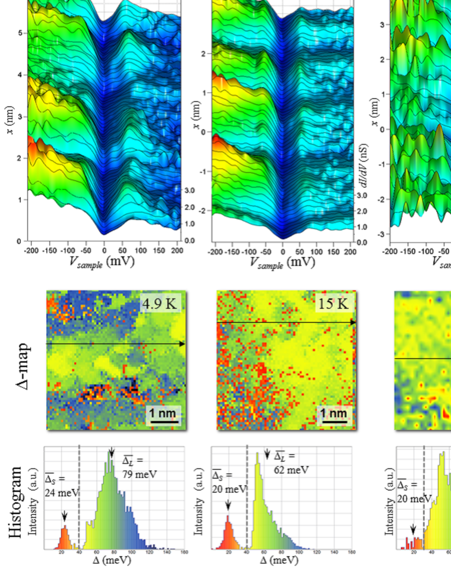
To obtain more insight into the origin and character of these multiple-gap spectra, we visualize the two-dimensional (2D) spatial gap distribution ( map) obtained from the measurements, like those shown in Figs. 2(c)(e). In Fig. 3(a), we depicted the map created at 4.9 K and corresponding to the STM image area of Fig. 2(a). The values were defined by the lowest peak locations at the positive bias branch. If there were two gap peaks for a single spectrum, the map point is attributed to the lower one value rather than to the larger one . Hence, the map includes both gap values, namely, and . In Fig. 3(b), such points that correspond to the multiple-gap spectra are indicated by the gray-scaled pixels. We note that some curves exhibit the peculiarity at the smaller gap location as a kink rather than the coherence peak at the gap edge. Such features were not included into the map of Fig. 3 (b). The distribution including the kink structures () will be shown and discussed later. (See Fig. 6 (a-1).) The map sections corresponding to the multiple-gap electron spectrum were much smaller than the single-gap areas. Fig. 3(c) includes the spatial distribution of ( map) defined by the maximum-peak voltage at the positive bias branch, as is shown in Fig. 2(b) by the arrow and notation . The map exhibits the distribution similar to that appropriate to the general map shown in Fig. 3(a). In addition, the map reveals patch-like structures with a smooth spatial variation, which are similar to that found for Bi-based and some other families of cuprate superconductorscampi15:359 . However, in contrast to the latter, one can recognize that the length scale of the spatial variation depicted in Fig. 3 is rather small, about 1 nm. This length scale is comparable to that of the spot structures, as is seen in the topography of Fig. 2(a). The character of the gap-distribution length scale will be discussed in more detail below. The histogram of map (Fig. 3(a)) is shown in Fig. 3(d). One can readily see that this histogram has a structure with distinct two-peaks, as is indicated by the two arrows in Fig. 3(d). Such a form testifies that the and are entirely separated at the dividing energy of meV, so that both distributions should be associated with different types of gaps. The partitioning into low and high energy gaps of non-similar nature is well-known for cuprates, where high-energy gaps are traditionally called pseudogapshufner08:062501 ; kordyuk15:417 ; yoshida16:014513 and are most probably the consequence of the charge density wave (CDW) formation, recently observed by various methodsgabovich16:1103 ; ekino16:445701 . The distribution is rather wide, in the range from = 40 mV to 140 mV. The average value of the smaller is 24 meV with the standard deviation 5 meV, while that of the larger one is 79 meV with 17 meV. Figures 3(a) and 3(b) demonstrate that the -covered area in the map consists of disconnected fragments covering only about % of the whole surface. This small area is shown in Fig. 3(c) as dark spots distributed inside the major -covered area.
The temperature-dependent STS measurement results are presented in Fig. 4. They include the typical line spectra, maps, and the -map histograms, depicted in upper, middle, and bottom panels, respectively. The selected values are (a) 4.9, (b) 15, (c) 45, (d) 60, and (e) 77 K, thus including temperatures both below and above . The relevant notations are the same as those of Fig. 3 (a). The spectra were measured for 64 64 points at 4.9 and 15 K, while at 45, 60, and 77 K the number of points was reduced to 32 32 in order to maintain the stable measurement conditions. The results obtained at 4.9 K and represented in Fig. 4(a) are the same as in Fig. 3 and are included once more for comparison. The locations of the profile sets for each upper panel are indicated by black arrows in the corresponding maps (middle panels). The line profiles of Fig. 4(b) ( K) demonstrate the clear-cut peak structures at as recognizable as those for 4.9 K. Similarly, the histogram at 15 K reveals the double-peak gap distributions (lower and higher ) with the border energy of meV, which are as clearly observed as same as those at 4.9 K. The average values of the relevant gaps are ( 15 K) 20 meV and ( 15 K) 62 meV. On the other hand, the line spectra at 45 K and 60 K are thermally smeared but the gap peaks still can be recognized at about 50 mV. The histogram at 60 K also exhibits the double-peak distribution, with the energy of meV being an approximate point dividing and . If we accept the border between and distributions as =30 meV, the average values of the gaps involved become (45 K) 20 meV, (60 K) 17 meV, (45 K) 63 meV, and (60 K) 65 meV. In Fig. 4 (e), the STS results are shown for 77 K, i.e. above . The corresponding spectra reveal large shallow depressions with remnants of broad gap peaks around 100 mV. From the histogram at 77 K, the average gap can be estimated as (77 K) 104 meV. At the same time, the histogram at 77 K shows no traces of the double-peak patterns. Since vanishes above , it is reasonable to suggest that it is the true superconducting gap, whereas the interpretation of the other gap , which survives in the normal state, needs further discussion.
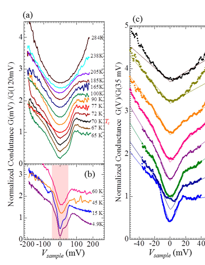
In order to accurately obtain the dependence of , it is necessary to measure the temperature evolution of curves both below and above the critical temperature, smoothly crossing this crucial point. The results of such measurements carried out in the bias voltage range of 200 mV and the range of 4.9 K to 284 K are depicted in Figs. 5 (a) and (b). In Fig. 5(b), the presented curves were derived by averaging the whole measured set of Figs. 4(a) to 4(d). Each curve shown in Figs. 5 (a) and (b) was obtained by dividing the measured conductance by 120 mV (mV)=1 at mV). For clarity of the comparison, the curves were offset. Looking at Fig. 5(a), one can clearly recognize that the LDOS depletion associated with the large indeed survives far above up to about 200 K. The persistence of the gap-like electron spectrum behavior above is consistent with the indicated above pseudogaps, which clearly manifest themselves in Bi-based cuprate superconductors keimer15:179 ; yazdani ; ekinoBi ; matsuda2 ; kordyuk15:417 ; kurosawa10:094519 .
The evolution in the range 4.9 K to 70 K of averaged spectra is shown in Fig. 5(c) for low bias voltages 40 mV, including the range where the smaller (superconducting) gap clearly manifests itself. This data set makes it possible to find the dependence of sugimotoPhysC_ISS2008 . In order to make results quantitative, our experimental dependencies were fitted by the theoretical formula for the tunnel conductance. Namely, the fitting curves were based on the basic Dynes phenomenological functiondynes78:1509 . However, the latter was modified by the weighting function reflecting the adopted -wave superconducting order parameter symmetrywon94:1397 and with an additional function making allowance for the linear background function manifesting itself for cuprateskirtley92:336 ,
| (1) |
where and are the Dynes broadening parameter and a constant, respectivelysugimotoPhysC_ISS2008 . The variable is the angle measured from the anti-nodal line on the 2-dimensional CuO2 plane. Thin solid lines in Fig. 5(c) correspond to the fitting curves at each temperature.
At 4.9 K, the fitting results are as follows: = 14.7 meV, = 4.4 meV and (V-1). As increases, the calculated superconducting gap remains almost constant up to 40 K, for example, (10 K) = 15 meV and (40 K) = 16 meV. However, above = 50 K, -related peculiarities in the curves are quickly smeared and the value of begins to gradually decrease. In Fig. 5(d), the values found at various temperatures are plotted by solid diamonds. The dashed line in Fig. 5(d) represents the dependence of the gap given by the conventionally reduced BCS theory, which (in this coordinates) is quite similar for -wave and -wave symmetries of the order parametervoitenko10:20 . One sees that the curve follows the -wave weak-coupling BCS law of the corresponding stateswon94:1397 (the dashed curve). The magnitudes of the and are plotted together in Fig. 5(d) as the open diamonds and the open triangles, respectively, showing that slightly decreases with growing , while exhibits no conspicuous changes in the range 4.9 K 60 K. All the fitting values of are smaller than the averaged ones . At the same time, the empirical relationship Ekino_Bi_PhysRevB1989 is approximately valid for the results obtained. The role of broadening factors was also discussed in more detail for tunnel measurements of superconducting -KxTiNCl and -HfNClysugimotoPRBMNCl . The huge discrepancy between and cannot be understood on the basis of the dissipation-related broadening and its thermal counterpart. Thus, its nature remains obscure. That is why we considered reasonable to analyze rather than to elucidate the actual temperature dependence of the gap , whatever broadening and disorder factors influence the gap-value distributions. Hence, a true superconducting energy gap identified with the calculated takes the value 15 meV at . This leads to the gap ratio 2 4.9, which apparently exceeds the weak-coupling values of this important mean-field parameter both for and -wave superconductors. It means that the strong-coupling effects are important although not crucial in our case, so that the use of the phenomenological treatmentdynes78:1509 is justified. Here, is the Boltzmann constant. The value of this benchmark ratio 4.9 is smaller than that of Bi2Sr2CaCu2O8+δ (Bi2212, = 7 10) or La2-xSrxCuO4 (= 5 10), but is comparable to that of YBa2Cu3Oy (= 4 6) and electron-doped Ln2-xCexCuO4 (= 4 7, Ln= lanthanides) sugimotoPRB2006 ; ekinoNCCO ; zimmers ; kato ; maki . The unusually small ratio as compared to that of the similar Bi2212 may be associated with difference in inhomogeneous and distributions or to the change of the ratio 2 due to the influence of the pseudogap (CDW gap) gabovich10:681070 .
The dependences of the larger gap are depicted in the upper part of Fig. 5(d). There are two kinds of the measured quantities, which may represent the actual gap. The first one is , being the averaged value from the histogram describing the group of Figs. 4 (red-open triangles), and the other one (red-solid triangles) is directly obtained as the outer peak voltage at the positive bias of the averaged curve, such as shown, e.g., in Fig. 5 (a). It comes about that the gap persists both below and above 70 K and its magnitude increases from 60 to 110 meV with growing . In analogy with Bi-based cuprates, the quantity is suspected to be a pseudogap (CDW gap) competing with superconductivitygabovich10:681070 ; kordyuk15:417 ; gabovich16:1103 ; voitenko10:20 . Hence, the initial increase of when superconductivity is suppressed near is quite natural. On the other hand, the further continuous enhancement of at higher temperature is counterintuitive, since in the mean-field scenario the CDW order parameter behaves similarlygruner94:book to its superconducting analog, which was clearly observed, e.g, for dichalcogenidesshen07:216404 and trichalcogenidessinchenko99:4624 ; ekino1986 . It should be noted that the growth of the PG with far above was also observed for Bi(Pb)2Sr2Ca(Tb)Cu2O8+δkordyuk09:020504 . However, in the latter material the enhancement gave way to the decrease at ever larger temperatures, making nonmonotonic the overall PG behavior. Peculiarities intrinsic to the presented here larger gap dependence as well as data of Ref. [kordyuk09:020504, ] might be caused either by the unusually strong dielectric order parameter fluctuations in those quasi-two-dimensional oxides kivelson03:1201 ; fradkin15:457 or the interplay between the pseudogap and CDW gaps being different phenomena in this case, coexisting in the non-superconducting region of the phase diagramkeimer15:179 ; kordyuk15:417 . This speculation is supported by the recent observation of the CDW-gap nonmonotonic behavior (analogous to that found in high- oxideskordyuk09:020504 ) in the superconducting layered dichalcogenide -NbSe2 as wellborisenko09:166402 . The very interpretation of the gap in F0256 as the CDW one is tentative and is based on the analogy between this superconducting cuprate and its analogues, where CDWs were first guessed to exist and later on discovered directly by x-ray scattering. For instance, CDWs were discovered in YBa2Cu3O7-δachkar12:167001 ; forgan15:10064 . By CDWs in cuprates we mean not only charge-carrier static waves but also the concomitant periodic lattice distortions minimizing together the free energy of the whole metallic system gruner94:book ; rossnagel11:213001 .
In Fig. 5(d), one can easily see the difference in energy between and , specifically, is about 4 to 5 times larger than . However, in contrast to , which in the usual way disappears below the critical temperature of the superconducting transition K, the competing gap survives in the normal state, up to 200 K. We note, that this is in line with the pseudogap (the CDW gap, in our interpretationgabovich10:681070 ; gabovich16:1103 ; voitenko10:20 ) behavior in a number of cuprate superconductors, especially in Bi-based ones, when the larger gap manifests itself above , as was confirmed by various experimental methods keimer15:179 ; yazdani ; ekinoBi ; matsuda2 ; hufner08:062501 ; kordyuk15:417 ; yoshida16:014513 ; mesaros16:1266 . In particular, in our previous break-junction (BJ) tunneling experiment, the temperature dependence of the normal-state gap magnitude varied up and down in the neighborhood and persisted up to almost the room temperature ekinoBi .
As was mentioned above, the magnitudes of both relevant gaps in high- oxides demonstrate substantial spatial scatterhowald ; kmlang ; matsuda1 ; mcelroy ; sugimotoPRB2006 ; machida ; fischer07:353 ; boyer2201 ; zeljkovic ; miyakawa05:225 ; gabovich16:1103 ; ekino16:445701 . In our samples, the length scale of the variation, especially that of the is very small. In order to clarify the correlation between the spot structures in the topography and the spatial variations, the continuous spatial variations of also should be explored. However, the peak is so small that the distribution of is discrete. Hence, we additionally-estimate the distribution of including the “kink” structure , which was not taken into account in the map of Fig. 3(b). The definition of the value is the inflection point of the kink structure around = +540 meV. Fig. 6 (a-1) displays the map on the squared area of the topography of Fig. 2 (a) and is shown together with with the contour plots of the topography. The map with the contour plots of the topography is also depicted in Fig. 6(a-2), reproducing the bottom part of Fig. 3 (c). The line-cut profiles of and taken at the same positions along the arrows shown in Figs. 6(a-1) and (a-2) are plotted in Fig. 6(b) along with the topography profiles. The was seen uniformly in the almost whole area except several positions of the spot structure. These results indicate that the quantity truly characterizes the superconducting states and is homogeneously distributed, while the larger gap is quite inhomogeneous and seems to be affected by the spot structures. As stems from the profile plots, the values do not exactly correlate with the topography height. For instance, the spot position A is in the small- region, while the spot B is found in the large- area. However, the steep spatial variation of does occur in the neighborhood of the spot structures. Thus, the gap is strongly influenced by spot structures contrary to its counterpart . Hence, the disorder appropriate to the BaO/F layers strongly modifies the pseudogap, while the superconducting gap of is not conspicuously influenced. It means that the sample inhomogeneity is linked to the non-homogeneous spatial distribution of the pseudogaps, the latter proven previously to be intrinsic to Bi-based ceramicsboyer2201 . To treat the spatial inhomogeneity of quantitatively, we estimated the full width at the half-maximum height (FWHM) of the map autocorrelation, . It turned out that the typical characteristic length is about 0.4 nm. For comparison, we also estimated from our previous results concerning maps of Bi2212 and Bi2201 (Bi2+xSr2-xCuO6+δ) cuprate superconductorssugimotoPRB2006 . All estimations are displayed on the - plane in Fig. 6(c). It is clear from this comparison that the characteristic length of F0256 is much shorter than that of Bi-based cuprate superconductors, i.e. by the factor of 1/2 to 1/3. Such a short characteristic length seems unexpected, because the spatial-inhomogeneity features of the gap distribution in F0256 turned out to be correlated with the spot structures rather than the superconducting coherence length (several nano-meters).
As was indicated above, the spot structures in F0256 were due to the non-replaced apical oxygen, as comes about from the comparison between the spot number and the O/F ratio. Therefore, these results indicate that the inhomogeneity should not be associated with superconductivity but is due to some other reasons, such as disorder of BaO/F layers. Recently, Zeljkovic showed that the disordered excess oxygens outside the CuO2 planes behave as the scattering centers and stabilize the pesudogap in Bi2212 zeljkovic . From this, quite reasonable, point of view, one should consider the non-superconducting gap (pseudogap or CDW gap) as strongly affected by the non-replaced oxygen driving the disorder outside of the CuO2 plane, so that the quantity correlates spatially with the spot structures. Generally speaking, STM/STS measurements probe the surface properties, i.e. mainly those of the outer plane in the studied case. In the F0256 compound under investigation, the disorder is a result of the replacements of apical O/F in the charge reservoir layer of BaO/F, as can be seen from the appearance of spot structures in STM topographies. Therefore, outer planes are affected by the disorder of the charge reservoir layer. Hence, the STS results are strongly influenced by the properties of the outer plane. That is why the order parameter inhomogeneity, i.e the existence of the dispersion () becomes strongly enhanced. One can make a conclusion that the length scale of the electronic inhomogeneity found in cuprate superconductors, including both the Bi-based and the apical Fluorine ones, originates from the atomic disorder distributions of the type observed here.
We note here that the magnitudes of gaps are relatively large as compared with those of Bi-based cuprates. For example, the averaged value of the large gap in F0256 is meV, while that in the typical optimally doped Bi-based oxide is about meV and that in the underdoped one is about meV fujita2012 . The multi-layered crystal structure of F0256 can be one of the possible reasons of such a discrepancy (see Fig. 1(a)). Indeed, the studied F0256 superconductor has 6 CuO2 planes in the unit cell. From the crystal structure of Fig. 1(a), one sees that there are three types of the inequivalent CuO2 planes, the topmost outer plane nearest to the BaO/F layer (OP), the next inner plane (IP1), and the most inner plane (IP2). According to the NMR studies of multi-layered cuprates, each CuO2 plane possesses a different carrier concentration determined by the distance from the charge reservoir layer of BaO/F, i. e. the inner CuO2 planes have lower carrier density than that of outer CuO2 planes shimizuNMR_PRL2007 ; mukuda12:011008 . In such multi-layered systems, the carrier concentrations per CuO2 plane are reduced. The gap magnitude, in general, becomes larger with decreasing carrier concentrations in cuprate superconductors, i.e. in underdoped compositions when the samples gradually approach the insulating state. In fact, according to the recent STS experiments on strongly underdoped Bi2212hamidian16:Nphys3519 , the averaged curve is very similar to ours, namely, demonstrating the existence of a very large gap peak 100 meV together with the small gap (kink) signal of of 30 meV.
Let us further discuss the existence of multiple gaps in F0256 superconductor. In the histograms of Fig. 4, only two-peak distributions can be found rather than triple-peak ones, although the F0256 compound possesses 3 types of nonequivalent CuO2 planes. Similar multiple-gap features were reported for a number of other cuprate superconductorsboyer2201 ; miyakawa05:225 . For instance, in the case of Pb-doped Bi2201 oxide, the two-gap patterns were reported, the smaller and larger gap being about 6.7 1.6 meV and 16 8 meV, respectivelyboyer2201 . The ingenious trick made it possible to elucidate that the larger gap (the pseudogap) is really inhomogeneous, whereas the inhomogeneity of the smaller (superconducting) gap is rather weakboyer2201 Our results also demonstrate that the distribution of the quantity is rather homogeneous, while the pseudogap is quite inhomogeneous, indicating that the superconductivity is quite spatially homogeneous against the inhomogeneous pseudogap background. It should be noted that the previous point-contact spectroscopy revealed the multiple- (triple- or more) gap structure of the electron spectrum, including the superconducting and pseudogap featuresmiyakawaPCF0234 . On the contrary, our results show only the double-peak structures. This discrepancy reflects the difference in the experimental configurations. Indeed, the STM surface-sensitive measurements detect mainly one or several topmost surfaces. In particular, our STS experiment seems to probe only the outer CuO2 plane of the exposed surface. On the other hand, point-contact studies detected all CuO2 planes in the unit cell, including inner and outer planes. Therefore, their curves revealed three or more kinds of gaps. Previous ARPES studies of the F0234 samples demonstrated the double Fermi surfaces, which was interpreted as the self-doping, the bilayer splitting being associated with the two different types of CuO2 planes, inner and outer ones chenARPES . However, our STS investigations of the F0256 oxide showed no evidence of such splitting for energies in the vicinity of . Nevertheless, the energy-gap edge of 85 meV found in the ARPES measurementschenARPES is consistent with our STS large-gap data meV at 4.9 K.
IV Summary
The STM/STS measurements of the multi layered cuprate superconductor Ba2Ca5Cu6O12(O1-xFx)2 (F0256) were carried out. The STM topography revealed random spot structures with the spatial scale of nm. The conductance spectra were shown to include two kinds of gap features The first, smaller, peculiarity corresponds to the superconducting gap , while the other one characterizes the larger gap, i.e. pseudogap , indicating the coexistence of superconductivity and pseudogap states down to low temperatures far below within the spatial interval of 0.07 nm. The fitting of the averaged curves in the low-voltage, superconducting region, leads to the value meV at K. The dependence of approximately follows the BCS dependence, resulting in the value about 4.9 of the hallmark ratio 2, being smaller than those characterizing other cuprates. The pseudogap observed at low temperatures below 70 K survives above as well. It increases with from the energy of meV to 110 meV, persisting up to 200 K. The -dependence of the map below the including small and large was constructed. From the histogram of the map, the averaged values at K were found to be meV and meV. The histogram above shows no traces of the double-peak distributions. Only the broad distributions with 104 meV are observed, clearly indicating that is the superconductive gap. The spatial distribution of is obtained by means of studying the kink structure of curves ( map). The shows almost spatially homogeneous distribution, while the pseudogap is quite inhomogeneous, possibly due to the disorder severely affecting the pseudogap-related phenomena. The maps exhibit the very short characteristic length nm. The spatial variation of is correlated with the length scale of the spot structures. This fact is in favor of the being strongly affected by the disorder of the apical O/F.
Acknowledgment
We would thank the Natural Science Center for Basic Research and Development (N-BARD), Hiroshima University for supplying cryogen (liquid helium) and the EPMA element analysis. This research was supported by JSPS KAKENHI Grant Numbers JP19540370, JP245403770, and the Project N24 of the 2015-2017 Scientific Cooperation Agreement between Poland and Ukraine.
References
- (1) R. A. Klemm, Layered Superconductors, Volume 1 (University Press, Oxford, 2012).
- (2) J. E. Hirsch, M. B. Maple, F. Marsiglio, Physica C, 514, 1 (2015).
- (3) J. Nagamatsu, N. Nakagawa, T. Muranaka, Y. Zenitani, J. Akimitsu, Nature (London) 410, 63 (2001).
- (4) Y. Kamihara, T. Watanabe, M. Hirano, H. Hosono, J. Am. Chem. Soc. 130, 3296 (2008).
- (5) H. Hosono, K. Kuroki, Physica C, 514, 399 (2015).
- (6) Y. Kubozono, R. Eguchi, H. Goto, S. Hamao, T. Kambe, T. Terao, S. Nishiyama, L. Zheng, X. Miao, H. Okamoto, J. Phys.: Condens. Matter., 28, 334001 (2016).
- (7) A. P. Drozdov, M. I. Eremets, I. A. Troyan, V. Ksenofontov, S. I. Shylin, Nature, 525, 73 (2015).
- (8) J. G. Bednorz, K. A. Muller, Z. Phys. B 64, 189 (1986).
- (9) B. Keimer, S. A. Kivelson, M. R. Norman, S. Uchida, J. Zaanen, Nature, 518, 179 (2015).
- (10) A. A. Kordyuk, Fiz. Nizk. Temp., 41, 417 (2015) [Low Temp. Phys., 41, 319 (2015)].
- (11) H. Mukuda, S. Shimizu, A. Iyo, Y. Kitaoka, J. Phys. Soc. Jpn., 81, 011008 (2012).
- (12) V. Z. Kresin, S. A. Wolf, Rev. Mod. Phys., 81, 481 (2009).
- (13) H. Kamimura, H. Ushio, J. Supercond., 25, 677 (2012).
- (14) M. Hashimoto, I. M. Vishik, R-H. He, T. P. Devereaux, Z-X. Shen, Nat. Phys., 10, 483 (2014).
- (15) T. Das, R. S. Markiewicz, A. Bansil, Adv. Phys., 63, 151 (2014).
- (16) S. Hüfner, M. A. Hossain, A. Damascelli, G. A. Sawatzky, Rep. Prog. Phys., 71, 062501 (2008).
- (17) T. Yoshida, W. Malaeb, S. Ideta, D. H. Lu, R. G. Moor, Z-X. Shen, M. Okawa, T. Kiss, K. Ishizaka, S. Shin, S. Komiya, Y. Ando, H. Eisaki, S. Uchida, A. Fujimori, Phys. Rev., B 93, 014513 (2016).
- (18) R. A. Klemm, Phil. Mag., 85, 801 (2005).
- (19) J. R. Kirtley, C. R. Phys, 12, 436 (2011).
- (20) P. A. Lee, N. Nagaosa, X-G. Wen, Rev. Mod. Phys., 78, 17 (2006).
- (21) S. Tajima, Rep. Prog. Phys., 79, 094001 (2016).
- (22) J. Bardeen, L. N. Cooper, J. R. Schrieffer, Phys. Rev., 108, 1175 (1957).
- (23) H. Won, K. Maki, Phys. Rev., B 49, 1397 (1994).
- (24) C. Howald, P. Fournier, and A. Kapitulnik, Phys. Rev. B 64, 100504R (2001) , C. Howald, H. Eisaki, N. Kaneko, M. Greven, A. Kapitulnik, Phys. Rev. B 67, 014533 (2003).
- (25) K. M. Lang, V. Madhavan, J. E. Hoffman, E. W. Hudson, H. Eisaki, S. Uchida, and J. C. Davis, Nature (London) 415, 412 (2002).
- (26) A. Matsuda, T. Fujii, and T. Watanabe, Physica C 388-389, 207 (2003).
- (27) K. McElroy, J. Lee, J.A. Slezak, D. Lee, H. Eisaki, S. Uchida, J.C. Davis, Science 309, 1048 (2005).
- (28) A. Sugimoto, S. Kashiwaya, H. Eisaki, H. Kashiwaya, H. Tsuchiura, Y. Tanaka, K. Fujita, S. Uchida, Phys. Rev. B 74, 094503 (2006).
- (29) T. Machida, Y. Kamijo, K. Harada, T. Noguchi, R. Saito, T. Kato, and H. Sakata: J. Phys. Soc. Jpn. 75, 083708 (2006).
- (30) Ø. Fischer, M. Kugler, I. Maggio-Aprile, C. Berthod, Rev. Mod. Phys., 79, 353 (2007).
- (31) M. C. Boyer, W. D. Wise, K. Chatterjee, M. Yi, T. Kondo, T. Takeuchi, H. Ikuta, E. W. Hudson, Nature Phys 3, 802 (2007).
- (32) I. Zeljkovic, Z. Xu, J. Wen, G. Gu, R.S. Markiewicz, J.E. Hoffman, Science 337, 320 (2012).
- (33) A. M. Gabovich, A. I. Voitenko, Fiz. Nizk. Temp., 42, 1103 (2016) [Low Temp. Phys. 42, 863 (2016)].
- (34) J. C. Phillips, A. Saxena, A. R. Bishop, Rep. Prog. Phys., 66, 2111 (2003).
- (35) A. Damascelli, Z. Hussain, Z-X. Shen, Rev. Mod. Phys., 75, 473 (2003).
- (36) M. Vojta, Adv. Phys., 58, 699 (2009).
- (37) N. P. Armitage, P. Fournier, R. L. Greene, Rev. Mod. Phys., 82, 2421 (2010).
- (38) P. M. Shirage, D. D. Shivagan, Y. Tanaka, Y. Kodama, H. Kito, A. Iyo, Appl. Phys. Lett. 92, 222501 (2008).
- (39) A. Iyo, Y. Aizawa, K Y. Tanaka, M. Tokumoto, K. Tokiwa, T. Watanabe, H. Ihara, Physica C 357-360, 324 (2001).
- (40) A. Iyo, M. Hirai, K. Tokiwa, T. Watanabe, Y. Tanaka, Physica C 392-396, 140 (2003).
- (41) A. M. Gabovich, D. P. Moiseev, Fiz. Nizk. Temp., 4, 1115 (1978).
- (42) V. Z. Kresin, H. Morawitz, Solid State Commun., 74, 1203 (1990).
- (43) S. Shimizu, H. Mukuda, Y. Kitaoka, A. Iyo, Y. Tanaka, Y. Kodama, K. Tokiwa, T. Watanabe, Phys. Rev. Lett. 98, 257002 (2007).
- (44) N. Miyakawa, H. Haya, A. Iyo, Y. Tanaka, K. Tokiwa, T. Watanabe, T. Kaneko, Int. J. Mod. Phys. B 21, 3233 (2007).
- (45) Y. Chen, A. Iyo, W. Yang, X. Zhou, D. Lu, H. Eisaki, T.P. Devereaux, Z. Hussain, Z-X. Shen, Phys. Rev. Lett. 97 236401 (2006).
- (46) A. Sugimoto, K. Shohara, T. Ekino, Y. Watanabe, Y. Harada, S. Mikusu, K. Tokiwa, Y. Watanabe, Physica C 469, 1020 (2009).
- (47) A. Sugimoto, R. Ukita, T. Ekino, Y. Harada, T. Furukawa, K. Itagaki, K. Tokiwa, Physica C 471, 698 (2011).
- (48) T. Ekino, T. Takasaki, R.A. Ribeiro, T. Muranaka, J. Akimitsu, J. Phys.: Conf. Ser. 61, 278 (2007).
- (49) A. Sugimoto, T. Ekino, H. Eisaki, J. Phys. Soc. Jpn. 77, 043705 (2008).
- (50) A. Sugimoto, K. Shohara, T. Ekino, Y. Watanabe, Y. Harada, S. Mikusu, K. Tokiwa, Y. Watanabe, Physica C 470, S160 (2010).
- (51) A. Sugimoto, T. Ekino, K. Tanaka, K. Mineta, K. Tanabe, K. Tokiwa, Phys. Proc. 58, 71 (2014).
- (52) D. J. Derro, E. W. Hudson, K. M. Lang, S. H. Pan, J. C. Davis, J. T. Markert, A. L. de Lozanne, Phys. Rev. Lett.88, 097002-1 (2002).
- (53) Y.-F. Lv, W.-L. Wang, J.-P. Peng, H. Ding, Y. Wang, L. Wang, K. He, S.-H. Ji, R. Zhong, J. Schneeloch, G.-D. Gu, C.-L. Song, X.-C. Ma, Q.-K. Xue, Phys. Rev. Lett. 115, 237002 (2015).
- (54) M. H. Hamidian, S. D. Edkins, S. H. Joo, A. Kostin, H. Eisaki, S. Uchida, M. J. Lawler, E.-A. Kim, A. P. Mackenzie, K. Fujita, J. Lee, J.C. S. Davis,, Nat. Phys. 12, 150 (2016).
- (55) A. M. Gabovich, A. I. Voitenko, T. Ekino, Mai Suan Li, H. Szymczak, M. Pekala, Adv. Cond. Mater. Phys., 2010, 681070 (2010).
- (56) G. Campi, A. Bianconi, N. Poccia, G. Bianconi, L. Barba, G. Arrighetti, D. Innocenti, J. Karpinski, N. D. Zhigadlo, S. M. Kazakov, M. Burghammer, M. v. Zimmermann, M. Sprung, A. Ricci, Nature, 525, 359 (2015).
- (57) T. Ekino, A. M. Gabovich, Mai Suan Li, H. Szymczak, A. I. Voitenko, Journ. Phys.: Condens. Mater., 28, 445701 (2016).
- (58) M. Vershinin, S. Misra, S. Ono, Y. Abe, Y. Ando, A. Yazdani, Science 303, 1995 (2004).
- (59) T. Ekino, Y. Sezaki, H. Fujii, Phys. Rev. B 60 6916 (1999), T. Ekino, S. Hashimoto, T. Takasaki, H. Fujii, Phys. Rev. B 64, 092510 (2001).
- (60) A. Matsuda, S. Sugita, T. Watanabe, Phys. Rev. B 60, 1377 (1999).
- (61) T. Kurosawa, T. Yoneyama, Y. Takano, M. Hagiwara, R. Inoue, N. Hagiwara, K. Kurusu, K. Takeyama, N. Momono, M. Oda, M. Ido, Phys. Rev., B 81, 094519 (2010).
- (62) R. C. Dynes, V. Narayanamurti, J. P. Garno, Phys. Rev. Lett., 41, 1509 (1978).
- (63) J. R. Kirtley, S. Washburn, D. J. Scalapino, Phys. Rev., B 45, 336 (1992).
- (64) A. I. Voitenko, A. M. Gabovich, Phys. Solid State, 52, 18 (2010).
- (65) T. Ekino, J. Akimitsu, Phys. Rev. B 40, 6902 (1989).
- (66) A. Sugimoto, K. Shohara, T. Ekino, Z. Zheng, S. Yamanaka, Phys. Rev. B 85, 144517 (2012).
- (67) T. Ekino, A. Sugimoto, S. Hino, K. Shohara, A. M. Gabovich, J. Phys.: Conf. Ser. 150 052046 (2009).
- (68) A. Zimmers, Y. Noat, T. Cren, W. Sacks, D. Roditchev, B. Liang, R.L. Greene, Phys. Rev. B 76, 132505 (2007).
- (69) T. Kato, S. Okitsu, H. Sakata, Phys. Rev. B 72, 144518 (2005).
- (70) M. Maki, T. Nishizaki, K. Shibata, T. Sasaki, N. Kobayashi, Physica C 357-360, 291 (2001).
- (71) G. Grüner, Density Waves in Solids (Addison-Wesley, Reading, Massachusetts, 1994).
- (72) D. W. Shen, B. P. Xie, J. F. Zhao, L. X. Yang, L. Fang, J. Shi, R. H. He, D. H. Lu, H. H. Wen, D. L. Feng, Phys. Rev. Lett., 99, 216404 (2007).
- (73) A. A. Sinchenko, Yu. I. Latyshev, S. G. Zybtsev, I. G. Gorlova, P. Monceau, Phys. Rev., B 60, 4624 (1999).
- (74) T. Ekino, J. Akimitsu, Jpn. J. Appl. Phys. 26-3, 625 (1987).
- (75) A. A. Kordyuk, S. V. Borisenko, V. B. Zabolotnyy, R. Schuster, D. S. Inosov, D. V. Evtushinsky, A. I. Plyushchay, R. Follath, A. Varykhalov, L. Patthey, H. Berger, Phys. Rev., B 79, 020504 (2009).
- (76) S. A. Kivelson, I. P. Bindloss, E. Fradkin, V. Oganesyan, J. M. Tranquada, A. Kapitulnik, C. Howald, Rev. Mod. Phys., 75, 1201 (2003).
- (77) E. Fradkin, S. A. Kivelson, J. M. Tranquada, Rev. Mod. Phys., 87, 457 (2015).
- (78) S. V. Borisenko, A. A. Kordyuk, V. B. Zabolotnyy, D. S. Inosov, D. Evtushinsky, B. Büchner, A. N. Yaresko, A. Varykhalov, R. Follath, W. Eberhardt, L. Patthey, H. Berger, Phys. Rev. Lett., 102, 166402 (2009).
- (79) A. J. Achkar, R. Sutarto, X. Mao, F. He, A. Frano, S. Blanco-Canosa, M. Le Tacon, G. Ghiringhelli, L. Braicovich, M. Minola, M. Moretti Sala, C. Mazzoli, R. Liang, D. A. Bonn, W. N. Hardy, B. Keimer, G. A. Sawatzky, D. G. Hawthorn, Phys. Rev. Lett., 109, 167001 (2012).
- (80) E. M. Forgan, E. Blackburn, A. T. Holmes, A. K. R. Briffa, J. Chang, L. Bouchenoire, S. D. Brown, R. Liang, D. Bonn, W. N. Hardy, N. B. Christensen, M. v. Zimmermann, M. Hücker, S. M. Hayden, Nature Commun., 5, 10064 (2015).
- (81) K. Rossnagel, Journ. Phys.: Condens. Mater., 23, 213001 (2011).
- (82) A. Mesaros, K. Fujita, S. D. Edkins, M. H. Hamidian, H. Eisaki, S.-i. Uchida, J. C. S. Davis, M. J. Lawler, E.-A. Kim, Proc. Natl. Acad. Sci. USA, 113, 12661 (2016).
- (83) K. Fujita, A.R. Schmidt, E.-A. Kim, M.J. Lawler, D.H. Lee, J.C.Davis, H. Eisaki, S. Uchida, J. Phys. Soc. Jpn., 81, 011005 (2012).
- (84) N. Miyakawa, K. Tokiwa, S. Mikusu, T. Watanabe, A. Iyo, J. F. Zasadzinski, T. Kaneko, Int. J. Mod. Phys., B 19, 225 (2005).