Antiferromagnetic Domain Wall as Spin Wave Polarizer and Retarder
As a collective quasiparticle excitation of the magnetic order in magnetic materials, spin wave, or magnon when quantized, can propagate in both conducting and insulating materials. Like the manipulation of its optical counterpart, the ability to manipulate spin wave polarization is not only important but also fundamental for magnonics. With only one type of magnetic lattice, ferromagnets can only accommodate the right-handed circularly polarized spin wave modes, which leaves no freedom for polarization manipulation. In contrast, antiferromagnets, with two opposite magnetic sublattices, have both left and right circular polarizations, and all linear and elliptical polarizations. Here we demonstrate theoretically and confirm by micromagnetic simulations that, in the presence of Dzyaloshinskii-Moriya interaction, an antiferromagnetic domain wall acts naturally as a spin wave polarizer or a spin wave retarder (waveplate). Our findings provide extremely simple yet flexible routes toward magnonic information processing by harnessing the polarization degree of freedom of spin wave.
Introduction.
Spintronics extends the physical limit of conventional electronics by harnessing the electronic spin, another intrinsic degree of freedom of an electron besides its charge. wolf_spintronics_2001 ; zutic_spintronics_2004 As a collective excitation of ordered magnetization in magnetic systems, spin wave (or magnon when quantized) carries spin angular momentum like the spin-polarized conduction electron. Different from the spin transport by conduction electrons, the propagation of spin wave does not involve physical motion of electrons. Therefore, spin wave can propagate in conducting, semiconducting, and even insulating magnetic materials without Joule heating, a troubling issue faced by the present day silicon-based information technologies. markov_limits_2014 The dissipation in the spin wave system is mainly due to the magnetic damping, which is much weaker than the electronic Joule heating, especially in magnetic insulators. kajiwara_transmission_2010 Magnonics is a discipline of realizing energy-efficient information processing that uses spin wave as its information carrier. kruglyak_magnonics_2010 ; lenk_building_2011 ; chumak_magnon_2015 Besides its low-dissipation feature, the wave nature and the wide working frequency range of spin wave make magnonics a promising candidate of upcoming beyond-CMOS (Complementary Metal Oxide Semiconductor) computing technology.
Similar to the intrinsic spin property of elementary particles, polarization is an intrinsic property of wave-like (quasi-)particles such as photons, phonons, and magnons. It is more natural to encode information in the polarization degree of freedom than other degrees of freedom such as amplitude or phase. For instance, photon polarization has been widely used in encoding both classical and quantum information, bennett_quantum_2000 and manipulation of photon polarization is essential for applications in photonics. Goldstein_2003_polarized The phonon polarization has also been used in encoding acoustic information for realizing phononic logic gates, sophia_phonon_2014 ; sklan_splash_2015 and for controlling magnetic domain walls. kim_mechanical_2016 In contrast, most magnonic devices proposed or realized so far mainly use the spin wave amplitude chumak_magnon_2014 ; vogt_realization_2014 ; garcia-sanchez_narrow_2015 ; lan_spin-wave_2015 ; wagner_magnetic_2016 ; yu_magnetic_2016 or phase hertel_domain-wall_2004 ; lee_conceptual_2008 ; klingler_design_2014 ; buijnsters_chirality-dependent_2016 ; louis_bias-free_2016 to encode information, and spin wave polarization is rarely used except in very few cases. cheng_antiferromagnetic_2016 The lack of usage of polarization in magnonics has reasons. With only one type of magnetic lattice, ferromagnets can only accommodate the right-circular polarization, hence there is simply no freedom in polarization manipulation. This situation is similar to the case of half-metal, which has only one spin spieces. fang_spin-polarization_2002 In other words, ferromagnet is a half-metal for spin wave. To overcome this disadvantage, a straightforward approach is to use antiferromagnets in manipulating spin wave polarization. In antiferromagnets, due to the two opposite magnetic sublattices, spin wave polarization has complete freedom as the photon polarization. Thus, antiferromagnet is a normal metal for spin wave with all possible polarizations. In comparison with the ferromagnets, besides gaining the full freedom in polarization, antiferromagnets also have numerous other advantages, such as the much higher operating frequency (up to THz) and having no stray field, etc. gomonay_spintronics_2014 ; jungwirth_antiferromagnetic_2016 Due to these merits, antiferromagnet is regarded as a much better platform for magnonics than ferromagnet gomonay_spin_2010 ; tveten_staggered_2013 ; tveten_antiferromagnetic_2014 ; cheng_antiferromagnetic_2016 . In order to unleash the full power of antiferromagnets in magnonics, however, it is highly desirable to have a simple yet efficient way in manipulating spin wave polarization, ideally in a similar fashion as in its optical counterpart.
In general, to be able to manipulate polarization with full flexibility, two basic devices are indispensable, i.e. the polarizer and retarder (waveplate). Hecht_Optics_1987 ; Goldstein_2003_polarized The former is to create a particular linear polarization, and the latter is to realize the conversion between circular and linear polarizations. The actual realization of these two building blocks relies on the types of the (quasi-)particle in question. For instance, for photon, an array of parallel metallic wires functions as an optical polarizer, Goldstein_2003_polarized and a block of birefringent material with polarization-dependent refraction indices acts as an optical waveplate. Hecht_Optics_1987
Here, we show theoretically and confirm by micromagnetic simulations that, utilizing the Dzyaloshinskii-Moriya interaction (DMI) existing in the symmetry-broken systems, dzyaloshinsky_thermodynamic_1958 ; moriya_anisotropic_1960 an antiferromagnetic domain wall serves as a spin wave polarizer at low frequencies and a retarder at high frequencies. Due to the extreme simplicity and tunability of a magnetic domain wall structure, the manipulation of spin wave polarization in magnonics becomes not only possible but also simpler and more flexible than its optical counterpart.
Results.
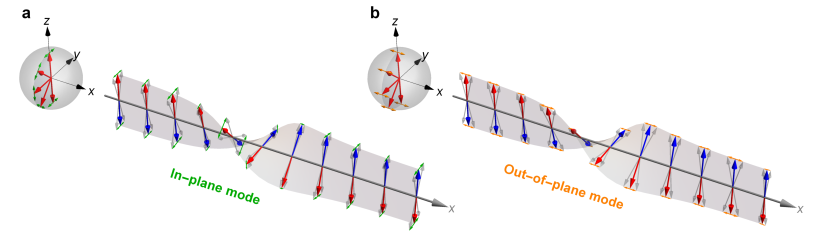
Model. We consider a domain wall structure in an one-dimensional antiferromagnetic wire along direction as shown in Fig. 1, where the red/blue arrows denote the magnetization direction for the two magnetic sublattices of an antiferromagnetic domain wall. The domain wall profile is taken as Bloch type, where the magnetization rotation plane (- plane) is perpendicular to the domain wall direction (). The magnetization dynamics in the antiferromagnetic wire can be described by two coupled Landau-Lifshitz-Gilbert (LLG) equations for each sublattice kittel_theory_1951 ; cheng_spin_2014 ,
| (1) |
where denote the two sublattices, is the gyromagnetic ratio, is the Gilbert damping constant. Here (with and ) is the effective magnetic field acting locally on sublattice , where is the easy-axis anisotropy along , and are the Heisenberg and Dzyaloshinskii-Moriya (DM) exchange coupling constant within each sublattice, and is the exchange coupling constant between two sublattices. The Heisenberg exchange coupling tends to align neighboring magnetization in parallel. While the DM exchange coupling, existing in magnetic materials or structures lack of spatial/inversion symmetry, dzyaloshinsky_thermodynamic_1958 ; moriya_anisotropic_1960 prefers magnetization to rotate counter-clockwise about an axis (-axis in our case) determined by the symmetry broken direction.
We denote the static profile of the antiferromagnetic domain wall along -axis as , and the stagger order , where and are the polar and azimuthal angle of with respect to (see Fig. 1). No matter DMI is present or not, an antiferromagnetic domain wall in Fig. 1 always takes the Walker type profile like its ferromagnetic counterpart with and , yan_all-magnonic_2011 ; lan_spin-wave_2015 ; tveten_antiferromagnetic_2014 where is the characteristic domain wall width. (See Supplementary Figure 1, Supplementary Note 1 and Supplementary Movie 1) The effect of DMI is to determine the domain wall type and chirality: when DMI is absent, the domain wall is free to take either the Bloch type () or Néel type () configuration, or any mixture of the two with ; in the presence of DMI, the domain wall becomes chiral chen_tailoring_2013 ; chen_novel_2013 and is pinned to the Bloch type as shown in Fig. 1.
With the static profile , let and be the dynamical spin wave excitation upon the static , where and are the local transverse (polar and azimuthal) directions with respect to . Since lies in the magnetization rotation plane (the - plane), we call the excitation in the in-plane mode. Similarly, the excitation in is perpendicular to the rotation plane and is called the out-of-plane mode (see Fig. 1). By eliminating the static profile from the LLG equation (1), the spin wave dynamics is governed by the following linearized LLG equations:
| (2) | ||||
| (3) |
where . The effects of the inhomogeneous domain wall texture are transformed into two effective potentials and : yan_all-magnonic_2011 ; lan_spin-wave_2015 arises due to the easy-axis anisotropy along , and is due to the combined action of DMI and the inhomogeneous magnetic texture. Equations (2)(3) can be regrouped into two independent sets for and , whose solutions are two linearly polarized spin wave modes oscillating in the (in-plane) -direction and (out-of-plane) -direction, respectively, as depicted in Fig. 1. Deep inside each domain (where ), the two transverse directions and coincide with and , therefore we also call the in-plane (out-of-plane) modes -polarized (-polarized) modes.
The influences of a domain wall on spin wave propagation are all captured by the effective potentials and . In the short wavelength limit (WKB approximation), using equations (2)(3), we may define the local dispersion at position for chosen polarization and wavevector :
| in-plane: | (4) | |||
| out-of-plane: | (5) |
which gives the local spin wave gap as , below which no in-plane/out-of-plane mode is allowed to propagate. In the absence of DMI (), the in-plane and out-of-plane modes are degenerate (). This degeneracy is lifted by the introduction of DMI (the term in equations (4)(5)), with which the local spin wave gap for the out-of-plane modes is higher than that for the in-plane modes inside the domain wall () (see the plots of the local spin wave gap in Fig. 2a). Deep inside each domain (), no matter whether DMI is present or not, both dispersions in equations (4)(5) reduce to the standard antiferromagnetic dispersion with a spin wave gap . kittel_theory_1951 ; keffer_theory_1952 It is seen that the dispersions inside domains is not modified by DMI, this is because that DMI modifies the spin wave dispersion with a linear term in wavevector only when the wavevector has component (anti-)parallel to the magnetization direction, zhang_plane_2015 and in our case the spin wave wavevector () is perpendicular to the magnetization direction ().
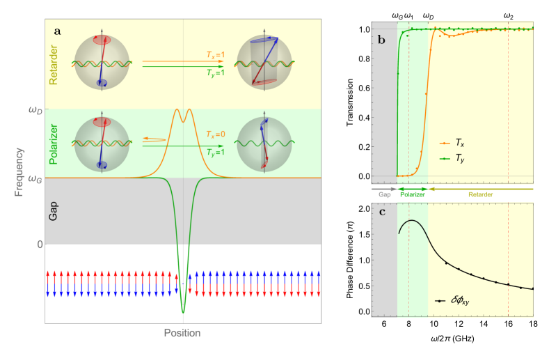
Polarization-dependent scattering. In the absence of DMI (), the dispersions and the local spin wave gaps for in-plane and out-of-plane polarization in equations (4)(5) are identical, thus the scattering behavior of spin waves by the domain wall is independent of polarization. Furthermore, the potential is the well known reflectionless Pöschl-Teller type potential well. yan_all-magnonic_2011 ; wang_magnon-driven_2015 ; lan_spin-wave_2015 ; yu_magnetic_2016 Consequently, regardless of its polarization, the incident spin wave experiences no reflection by the domain wall, and only accumulate a common phase delay. However, when DMI is present (), the dispersions and local spin wave gaps for the in-plane and out-of-plane modes are different. Considering that the inter-sublattice exchange coupling is the dominating energy scale in antiferromagnet, the in-plane gap is barely affected by (). On the contrary, the out-of-plane gap is elevated by and reaches its maximum value inside the domain wall. This effect of DMI in equations (4)(5) is equivalent to an effective hard-axis anisotropy along the out-of-plane () direction inside the domain wall thiaville_dynamics_2012 ; wang_magnon-driven_2015 , which suppresses the out-of-plane excitation. Consequently, the domain wall can still be regarded as reflectionless for the in-plane -polarization, but becomes a potential barrier of height for the out-of-plane -polarization (see Fig. 2(a)). Therefore, the - and -polarized modes are scattered differently: At low frequencies (), the -polarization experiences no (or little) reflection but the -polarization hits a potential barrier and is strongly reflected; At higher frequencies (), both polarization transmit almost perfectly, but the - and -polarization no longer share the same phase delay.
The polarization-dependence of the spin wave scattering behaviors by the domain wall are confirmed by micromagnetic simulations based on the LLG equations (1) and Green’s function calculations based on linearized LLG equations (4)(5). (See Supplementary Note 3 for details) Using these methods, we calculate the spin wave transmission probabilities through the domain wall for the linear - and -polarization, as well as their relative phase accumulation , as presented in Fig. 2(b,c). It is seen that the -polarization transmit almost perfectly () for all frequencies above the spin wave gap (). In contrast, because of the effective potential barrier, the -polarization experiences total reflection () at low frequencies (). Above the barrier (), however, the -polarization experiences little reflection (). Because of the different effective potentials experienced at the domain wall, the - and -polarizations develop a relative phase accumulation , which is frequency-dependent as shown in Fig. 2(c). All these behaviors are in perfect agreement with the qualitative understanding shown in Fig. 2(a). Utilizing these particular spin wave scattering properties, an antiferromagnetic domain wall can be used as a spin wave polarizer and retarder (or waveplate) as discussed in the following.
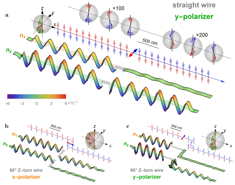
Spin wave polarizer. In the low frequency regime (), because the -polarized spin wave is totally reflected, an antiferromagnetic domain wall is naturally a -polarizer for spin wave. The functionality of the spin wave polarizer is confirmed by a micromagnetic simulation on a straight antiferromagnetic wire shown in Fig. 3a: when a circularly-polarized spin wave, consisting of - and -polarization of equal amplitude, is injected from the left side of the domain wall, only the -polarization transmits, indicating that the domain wall is a y-polarizer for spin wave.
It appears that the polarizer demonstrated in Fig. 3a can only be a -polarizer. In fact, an -polarizer can be realized simply by using a Z-turn wire as shown in Fig. 3b, where the domain wall is located at the central segment. Because the domain wall is now along the direction and the static magnetization rotates from to in the - plane (rather than the - plane in the straight wire case in Fig. 3a), roles of -polarization and -polarization interchange. Therefore, a domain wall located at the central segment of a Z-turn wire only allows the -polarization to pass (instead of the -polarization in the straight wire case), hence it is an -polarizer as demonstrated in Fig. 3b. Actually, a Z-turn wire can work as either - or -polarizer depending on the location of the domain wall: an -polarizer when the wall is at the center segment (Fig. 3b), and a -polarizer when the wall is at either the left (Fig. 3c) or right segment.
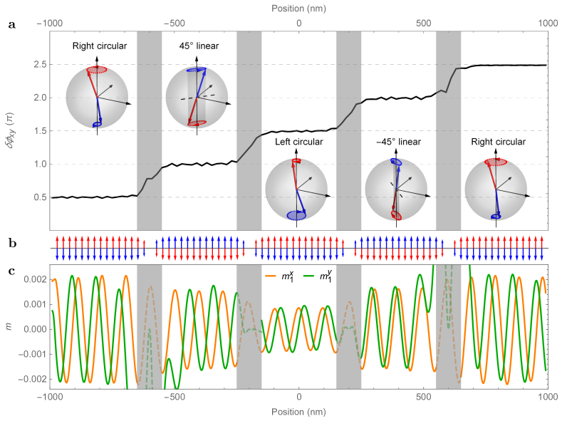
Spin wave retarder. In the high frequency regime (), both - and -polarized spin wave modes transmit almost perfectly through the domain wall, but they accumulate different phases. As a result of this relative phase delay, an antiferromagnetic domain wall functions as a spin wave retarder (or a waveplate). As shown in Fig. 2(c), the relative phase delay depends on the spin wave frequency. By choosing the working frequency at GHz, the relative phase delay between the - and -polarization , hence the antiferromagnetic domain wall is specifically a quarter-wave plate. Fig. 4 shows a micromagnetic simulation of a right-circularly polarized spin wave passing through four consecutive domain walls, each of which is a quarter-wave plate. As shown in the top panel, the relative phase delay increases by across each domain wall. By passing through these domain walls, the right-circular polarized spin wave is converted into a -linear mode, a left-circular mode, a -linear mode, and back into a right-circular mode, successively.
Discussion.
The antiferromagnetic domain wall based spin wave polarizer/retarder mimics its optical counterpart in many aspects. For example, the spin wave polarizer follows the Malus’s law Goldstein_2003_polarized as the optical polarizer, i.e. the spin wave intensity is reduced by with the angle between the injecting polarization and the polarizer direction. Owing to the relative phase delay, an antiferromagnetic domain wall with DMI can be regarded as a birefringent material for spin wave. This birefringence brought by magnetic texture here only occurs within the domain wall region, thus it is drastically different from the birefringence caused by the biaxial anisotropy with the polarization degeneracy lifted in the whole antiferromagnetic material. khymyn_transformation_2016 In addition, both polarizing and retarding effects are independent of propagation direction, or equivalently, an up-to-down domain wall and a down-to-up domain wall are the same in polarizing or retarding. All these features enable us to construct magnonic circuits in a similar fashion as the well-established optical circuits. murphy_integrated_1999 Beyond the capability of its optical counterpart, due to the extreme tunability of magnetic textures, e.g. creating/annihilating or moving a domain wall, the magnonic circuit built upon magnetic domain walls can be modulated with even greater flexibility. lan_spin-wave_2015
As demonstrated above in Fig. 3, a simple geometric modification (from a straight to a Z-turn wire) can change the polarizing behavior. This is because that the spin wave polarization is characterized in the spin space, and it does not change when the propagation takes turns in real space. However, the rotation plane of the magnetization of a domain wall depends on the domain wall direction in real space. Therefore, the polarization component allowed for transmission depends on the domain wall direction as seen in Fig. 3. Based on this principle, a linear polarizer along arbitrary direction can be realized straightforwardly using a wire with a turn of appropriate angle.
The polarizing and retarding effects sustains at smaller DMI strength (See Supplementary Figure 2 and Supplementary Note 2). For fixed material parameters ( etc), the working frequency range for the spin wave polarizer and retarder are different, i.e. a polarizer for and a retarder for . However, by modulating the material parameters (such as tuning the DMI strength as in zhang_electric-field_2014 ; ma_interfacial_2016 ), it is possible to have the spin wave polarizer and retarder functioning in the same frequency range. Henceforth, multiple polarizers (of different polarization direction) and retarders (of different phase delay) can be assembled into one magnonic circuit to realize more complex spin wave manipulations.
The DMI has two different forms, the bulk and the interfacial form, fert_skyrmions_2013 where the former is caused by the bulk inversion symmetry breaking, such as in MnSi tonomura_real_2012 and other B20 compounds kang_transport_2015 , and the latter is due to the interfacial inversion symmetry breaking, such as in Co/Pt or Co/Ni bilayer. yoshimura_soliton_2015 ; soumyanarayanan_emergent_2016 Here, we adopt the bulk form DMI to demonstrate the working principle of the spin wave polarizer and retarder. However, the materials or structures with interfacial form DMI would work in almost the same manner. The only difference is that interfacial DMI prefers a Néel type domain wall rather than a Bloch type for the bulk DMI, chen_tailoring_2013 ; chen_novel_2013 and the roles of in-plane and out-of-plane modes interchange. Besides the inhomogeneous DMI discussed above, there is also homogenous DMI that makes the antiferromagnet a weak ferromagnet by slightly misaligning the magnetizations in two sublattices. dzyaloshinsky_thermodynamic_1958 ; moriya_anisotropic_1960 However, such a misalignment is extremely small because of the dominating antiferromagnetic coupling, thus is ignored in our discussions.
The working principles for the spin wave polarizer and retarder work for both real antiferromagnet and artificial synthetic antiferromagnet, where the latter consists of two antiferromagnetically coupled ferromagnetic wires. saarikoski_current_2014 ; yang_domain_2015 The domain wall structures have been observed in both types of antiferromagnetic materials weber_magnetostrictive_2003 ; bode_atomic_2006 ; yang_domain_2015 , and can be effective controlled by using the exchange bias effects. mauri_simple_1987 ; kim_hysteresis_2005 ; nolting_direct_2000 ; logan_antiferromagnetic_2012 ; tveten_antiferromagnetic_2014 ; cheng_dynamics_2014 Experimentally, it should be more straightforward to realize the spin wave polarizer and retarder proposed here using the synthetic antiferromagnetic wires used for the racetrack memory. yang_domain_2015
In conclusion, we demonstrated that the antiferromagnetic domain wall with Dzyaloshinskii-Moriya interaction naturally functions as a spin wave polarizer at low frequency, and a spin wave retarder (waveplate) at high frequency. This extremely simple design enables all possible polarization manipulations for antiferromagnetic spin waves. Our findings greatly enrich the possibility of magnonic information processing by harnessing the polarization degree of freedom of spin wave.
Methods.
Micromagnetic Simulations. The micromagnetic simulations are performed in COMSOL Multiphysics, where the LLG equation is transformed into weak form by using the mathematical module and solved by the generalized-alpha method. The synthetic antiferromagnet wire is composed of two ferromagnetic YIG wires with the following parameters:yan_all-magnonic_2011 ; lan_spin-wave_2015 ; yu_magnetic_2016 the easy-axis anisotropy , the intra-sublattice Heisenberg exchange constant , the saturation magnetization , the gyromagnetic ratio , and the DMI constant . The inter-sublattice antiferromagnetic exchange coupling between two ferromagnetic wires is . The dipolar interaction is neglected for this antiferromagnetic environment. To obtain the transmission probability, we first verify that the spin wave perfectly transmits for , then the transmission probability for a chosen polarization is extracted by taking the ratio between the spin wave amplitude for i) and ii) at the location nm away from the domain wall.
Data availability. The data that support the findings of this study are available from the corresponding authors on request.
References.
References
- (1) Wolf, S. A. et al. Spintronics: A Spin-Based Electronics Vision for the Future. Science 294, 1488–1495 (2001).
- (2) Žutić, I., Fabian, J. & Das Sarma, S. Spintronics: Fundamentals and applications. Rev. Mod. Phys. 76, 323–410 (2004).
- (3) Markov, I. L. Limits on fundamental limits to computation. Nature 512, 147–154 (2014).
- (4) Kajiwara, Y. et al. Transmission of electrical signals by spin-wave interconversion in a magnetic insulator. Nature 464, 262–266 (2010).
- (5) Kruglyak, V. V., Demokritov, S. O. & Grundler, D. Magnonics. J. Phys. D: Appl. Phys. 43, 264001 (2010).
- (6) Lenk, B., Ulrichs, H., Garbs, F. & Münzenberg, M. The building blocks of magnonics. Phys. Rep. 507, 107–136 (2011).
- (7) Chumak, A. V., Vasyuchka, V. I., Serga, A. A. & Hillebrands, B. Magnon spintronics. Nat. Phys. 11, 453–461 (2015).
- (8) Bennett, C. H. & DiVincenzo, D. P. Quantum information and computation. Nature 404, 247–255 (2000).
- (9) Goldstein, D. Polarized Light Second Edition, Revised and Expanded, (Marcel Dekker, New York, 2003).
- (10) Sophia, R. S. & Jeffrey, C. G. Phonon diodes and transistors from magneto-acoustics. New J. Phys. 16, 053029 (2014).
- (11) Sklan, S. R. Splash, pop, sizzle: Information processing with phononic computing. AIP Advances 5, 053302 (2015).
- (12) Kim, S. K., Hill, D. & Tserkovnyak, Y. Mechanical actuation of magnetic domain-wall motion. Phys. Rev. Lett. 117, 237201 (2016).
- (13) Chumak, A. V., Serga, A. A. & Hillebrands, B. Magnon transistor for all-magnon data processing. Nat. Commun. 5, 4700 (2014).
- (14) Vogt, K. et al. Realization of a spin-wave multiplexer. Nat. Commun. 5, 3727 (2014).
- (15) Garcia-Sanchez, F. et al. Narrow magnonic waveguides based on domain walls. Phys. Rev. Lett. 114, 247206 (2015).
- (16) Lan, J., Yu, W., Wu, R. & Xiao, J. Spin-Wave Diode. Phys. Rev. X 5, 041049 (2015).
- (17) Wagner, K. et al. Magnetic domain walls as reconfigurable spin-wave nanochannels. Nat. Nano. 11, 432–436 (2016).
- (18) Yu, W., Lan, J., Wu, R. & Xiao, J. Magnetic Snell’s law and spin-wave fiber with Dzyaloshinskii-Moriya interaction. Phys. Rev. B 94, 140410 (2016).
- (19) Hertel, R., Wulfhekel, W. & Kirschner, J. Domain-wall induced phase shifts in spin waves. Phys. Rev. Lett. 93, 257202 (2004).
- (20) Lee, K.-S. & Kim, S.-K. Conceptual design of spin wave logic gates based on a mach-zehnder-type spin wave interferometer for universal logic functions. J. Appl. Phys. 104, 053909 (2008).
- (21) Klingler, S. et al. Design of a spin-wave majority gate employing mode selection. Appl. Phys. Lett. 105, 152410 (2014).
- (22) Buijnsters, F. J., Ferreiros, Y., Fasolino, A. & Katsnelson, M. I. Chirality-Dependent Transmission of Spin Waves through Domain Walls. Phys. Rev. Lett. 116, 147204 (2016).
- (23) Louis, S. et al. Bias-free spin-wave phase shifter for magnonic logic. AIP Advances 6, 065103 (2016).
- (24) Cheng, R., Daniels, M. W., Zhu, J.-G. & Xiao, D. Antiferromagnetic Spin Wave Field-Effect Transistor. Sci. Rep. 6, 24223 (2016).
- (25) Fang, C. M., de Wijs, G. A. & de Groot, R. A. Spin-polarization in half-metals (invited). J. Appl. Phys. 91, 8340–8344 (2002).
- (26) Gomonay, E. V. & Loktev, V. M. Spintronics of antiferromagnetic systems. Low Temp. Phys. 40, 17–35 (2014).
- (27) Jungwirth, T., Marti, X., Wadley, P. & Wunderlich, J. Antiferromagnetic spintronics. Nat. Nano. 11, 231–241 (2016).
- (28) Gomonay, H. V. & Loktev, V. M. Spin transfer and current-induced switching in antiferromagnets. Phys. Rev. B 81, 144427 (2010).
- (29) Tveten, E. G., Qaiumzadeh, A., Tretiakov, O. A. & Brataas, A. Staggered Dynamics in Antiferromagnets by Collective Coordinates. Phys. Rev. Lett. 110, 127208 (2013).
- (30) Tveten, E. G., Qaiumzadeh, A. & Brataas, A. Antiferromagnetic Domain Wall Motion Induced by Spin Waves. Phys. Rev. Lett. 112, 147204 (2014).
- (31) Hecht, E. Optics, (Addison-Wesley, New York, 1987).
- (32) Dzyaloshinsky, I. A thermodynamic theory of “weak” ferromagnetism of antiferromagnetics. J. Phys. Chem. Solids 4, 241–255 (1958).
- (33) Moriya, T. Anisotropic Superexchange Interaction and Weak Ferromagnetism. Phys. Rev. 120, 91–98 (1960).
- (34) Kittel, C. Theory of antiferromagnetic resonance. Phys. Rev. 82, 565–565 (1951).
- (35) Cheng, R., Xiao, J., Niu, Q. & Brataas, A. Spin pumping and spin-transfer torques in antiferromagnets. Phys. Rev. Lett. 113, 057601 (2014).
- (36) Yan, P., Wang, X. S. & Wang, X. R. All-Magnonic Spin-Transfer Torque and Domain Wall Propagation. Phys. Rev. Lett. 107, 177207 (2011).
- (37) Chen, G. et al. Tailoring the chirality of magnetic domain walls by interface engineering. Nat. Commun. 4 (2013).
- (38) Chen, G. et al. Novel Chiral Magnetic Domain Wall Structure in // Films. Phys. Rev. Lett. 110, 177204 (2013).
- (39) Keffer, F. & Kittel, C. Theory of antiferromagnetic resonance. Phys. Rev. 85, 329–337 (1952).
- (40) Zhang, V. L. et al. In-plane angular dependence of the spin-wave nonreciprocity of an ultrathin film with Dzyaloshinskii-Moriya interaction. Applied Physics Letters 022402 (2015).
- (41) Wang, W. et al. Magnon-Driven Domain-Wall Motion with the Dzyaloshinskii-Moriya Interaction. Phys. Rev. Lett. 114, 087203 (2015).
- (42) Thiaville, A. et al. Dynamics of Dzyaloshinskii domain walls in ultrathin magnetic films. Euro. Phys. Lett. 100, 57002 (2012).
- (43) Khymyn, R. et al. Transformation of spin current by antiferromagnetic insulators. Phys. Rev. B 93, 224421 (2016).
- (44) Murphy, E. J. Integrated optical circuits and components: Design and applications, (CRC Press, 1999).
- (45) Zhang, X., Liu, T., Flattè, M. E. & Tang, H. X. Electric-field coupling to spin waves in a centrosymmetric ferrite. Phys. Rev. Lett. 113, 037202 (2014).
- (46) Ma, X. et al. Interfacial control of dzyaloshinskii-moriya interaction in heavy metal/ferromagnetic metal thin film heterostructures. Phys. Rev. B 94, 180408 (2016).
- (47) Fert, A., Cros, V. & Sampaio, J. Skyrmions on the track. Nat. Nano. 8, 152–156 (2013).
- (48) Tonomura, A. et al. Real-space observation of skyrmion lattice in helimagnet MnSi thin samples. Nano Lett. 12, 1673–7 (2012).
- (49) Kang, J. & Zang, J. Transport theory of metallic B20 helimagnets. Phys. Rev. B 91, 134401 (2015).
- (50) Yoshimura, Y. et al. Soliton-like magnetic domain wall motion induced by the interfacial Dzyaloshinskii-Moriya interaction. Nat. Phys. 12, 157–161 (2016).
- (51) Soumyanarayanan, A., Reyren, N., Fert, A. & Panagopoulos, C. Emergent phenomena induced by spin-orbit coupling at surfaces and interfaces. Nature 539, 509–517 (2016).
- (52) Saarikoski, H., Kohno, H., Marrows, C. H. & Tatara, G. Current-driven dynamics of coupled domain walls in a synthetic antiferromagnet. Phys. Rev. B 90, 094411 (2014).
- (53) Yang, S.-H., Ryu, K.-S. & Parkin, S. Domain-wall velocities of up to 750 m s-1 driven by exchange-coupling torque in synthetic antiferromagnets. Nat. Nano. 10, 221–226 (2015).
- (54) Weber, N. B., Ohldag, H., Gomonaj, H. & Hillebrecht, F. U. Magnetostrictive Domain Walls in Antiferromagnetic NiO. Phys. Rev. Lett. 91, 237205 (2003).
- (55) Bode, M. et al. Atomic spin structure of antiferromagnetic domain walls. Nat Mater 5, 477–481 (2006).
- (56) Mauri, D., Siegmann, H. C., Bagus, P. S. & Kay, E. Simple model for thin ferromagnetic films exchange coupled to an antiferromagnetic substrate. J. Appl. Phys. 62, 3047–3049 (1987).
- (57) Kim, J.-V. & Stamps, R. L. Hysteresis from antiferromagnet domain-wall processes in exchange-biased systems: Magnetic defects and thermal effects. Phys. Rev. B 71, 094405 (2005).
- (58) Nolting, F. et al. Direct observation of the alignment of ferromagnetic spins by antiferromagnetic spins. Nature 405, 767–769 (2000).
- (59) Logan, J. M. et al. Antiferromagnetic domain wall engineering in chromium films. Appl. Phys. Lett. 100, 192405 (2012).
- (60) Cheng, R. & Niu, Q. Dynamics of antiferromagnets driven by spin current. Phys. Rev. B 89, 081105 (2014).
Acknowledgements. This work was supported by the National Natural Science Foundation of China under Grant No. 11474065, National Basic Research Program of China under Grant No. 2015CB921400 and No. 2014CB921600. J.L. is also supported by the China Postdoctoral Science Foundation under Grant No. KLH1512074. J.L. is grateful to Ran Cheng at Carnegie Mellon University for help with preparing figures.
Author Contributions. J.L. did the analytical calculations. W.Y. did the micromagnetic simulations. J.L. and W.Y. contributed equally to the work. J.X. planned and supervised the study. All authors discussed the results and worked on the manuscript.
Competing Financial Interests Statement. Fudan University filed two Chinese patent applications No. 2016112619740, No. 201611261990X based on the described technologies.