Analytical Solutions of Transient Drift-Diffusion
in P-N Junction Pixel Sensors
Abstract
Radiation detection in applications ranging from high energy physics to medical imaging rely on solid state detectors, often hybrid pixel detectors with (1) reverse biased p-n junction pixel sensors and (2) readout ASICs, attached by flip-chip-bonding. Transient signals characteristics are important in, e.g., matching ASIC and sensor design, modeling and optimizing detector parameters and describing timing and charge sharing properties. Currently analytical forms of transient signals are available for only a few limited cases (e.g., drift or diffusion) or for the steady state (which is not relevant for high energy radiation detection). Tools are available for (relatively slow) numerical evaluation of the transient charge transport. We present here the first analytical solutions of partial differential equations describing drift-diffusion-recombination charge transport in planar p-n junction sensors in a variety of conditions: (1) undepleted, (2) fully depleted, (3) taking into account the gradual velocity saturation, and (4) overdepleted. We deduce the Green’s functions which can be applied to any detection problem through simple convolution with the initial conditions. We compare the analytical solutions with Monte Carlo simulations and industry standard simulations (Synopsys Sentaurus), demonstrating good agreement. Using the analytical equations enables fast modeling of the influence of various detector parameters on tracking, imaging and timing performance, describing performance and enabling optimizations for different applications. Finally, we illustrate this model with applications in 3D+T (x,y,z,time) photon tracking and 4D+T (x,y,\texttheta,\textphi,time) relativistic charged particle tracking.
Index Terms:
Hybrid pixel detectors, p-n junction sensors, transient signals, charge transport, drift-diffusion-recombination model, partial differential equationsI Introduction
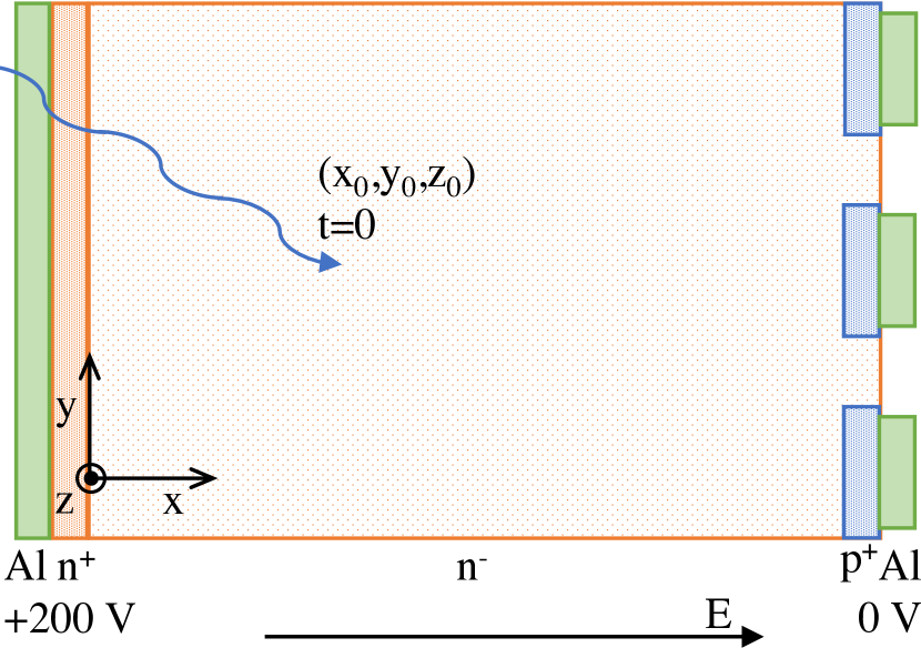
Radiation detection in applications ranging from high energy physics to medical imaging rely on solid state sensors (often silicon). The last three decades saw significant improvements in hybrid pixel detectors [1], which allow developing advanced functionality in the CMOS pixel readouts (e.g., digital photon counting [2, 3, 4], low noise charge integrating [5], spectroscopy [6, 7], timing [8, 9, 10], sparsification [9], gain switching [11, 12], other specialized functionality [13, 14]), while separating ASIC and sensor development and leveraging the commercial advances in chip fabrication. Most often, pixel sensors based on reverse biased p-n junctions are used [15] (see a schematic diagram in Fig. 1). Typical sensor materials include Si, GaAs, CdTe, Ge.
Currently the transient signals are analytically described for only a few special cases (e.g., simple thermal diffusion [16]). Steady state solutions are often presented [16, 17]; while they are useful in other applications (imaging at low energy, high flux, saturation, etc.), they are less relevant for discrete high energy quantum detection, where the steady state is trivial.
Often simulations [18] with technology computer-aided design (TCAD) packages are used [19], despite being relatively slow and requiring significant training. Other numerical approaches include finite elements: FEMOS [20], 2D Monte Carlo: Weightfield2 [21], simple assumptions about the charge transport: HORUS [22], or measurements and simulations of simple p-n diodes [23] with resulting limitations in speed, ease of use, and/or accuracy. These simulation tools typically require other software frameworks (e.g., IDL, Root) and, with the exception of Weightfield2, are not easily available.
We present here the first analytical solutions of partial differential equations describing drift-diffusion-recombination charge transport in planar p-n junction sensors in a variety of conditions: (1) undepleted, (2) fully depleted, (3) taking into account the gradual velocity saturation, and (4) overdepleted. We deduce the Green’s functions which can be applied to any detection problem through simple convolution with the initial conditions. We compare the analytical solutions with Monte Carlo simulations and industry standard TCAD simulations (Synopsys Sentaurus [24]), demonstrating good agreement.
Finally, we deduce equations governing transient charge transport and charge sharing, relating detection parameters (location and time, bias voltage, track orientation, and pixel geometry) and providing examples with 3D+T (x,y,z,time) photon tracking and 4D+T (x,y,\texttheta,\textphi,time) relativistic charged particle tracking. These analytical solutions enable fast modeling of the influence of various detector parameters on tracking, imaging and timing performance, describing performance and enabling optimizations for different applications.
II Reverse Biased p-n Junction Sensors
In radiation imaging with semiconductor pixel sensors, detection typically occurs in discrete events, resulting in concentrated electron-hole clouds around points or lines at the location and time of radiation interaction with the semiconductor sensor. These discrete clouds subsequently drift, diffuse and recombine until reaching the highly doped front or rear side contacts (Fig. 1).
The evolution of signals induced by individual photons or particles are non-equilibrium, non-steady-state processes in which the time evolution of charge carriers is important.
With high fluxes of radiation, the steady state solution can be useful. However, low noise radiation detection is usually measuring signals from single particles. In this case, the steady state solution is trivial, thus it is necessary to take into account the transient regime (i.e., spatio-temporal evolution of charge carrier concentrations).
II-A Sensors
Intrinsec semiconductors have relatively high thermal noise compared to signals induced by single x-ray photons [16]. To minimize the thermal noise, the sensor material can either be cooled to cryogenic temperatures (e.g., high purity germanium detectors) or used as a reverse biased p-n junction.
Most hybrid pixel sensors used in radiation detection are reverse biased p-n junctions, often a bulk n-type silicon sensor (thicknesses up to are common), with a thin ( p implant region. Fig. 1 shows a cross section of a typical n-type silicon sensor, with the front entrance window shown on the left, and several pixel readout contacts on the back plane shown on the right. Other sensor materials (e.g., CdTe, GaAs, Ge) can also be used.
The concentration of dopant in the n-type sensor bulk is related to the resistivity by [25]:
| (1) |
Usually the resistivity is quoted instead of the concentration of dopant. A typical value is , correspoding to a donor concentration of .
II-B Bias Voltage and Depletion
Applying a reverse bias voltage results in a fully depleted detector (i.e., over the entire detector width ), or partially depleted (i.e., depleted over width close to the readout and undepleted over a width close to the entrance window). We will call the sensor plane near the readout ASIC ”rear plane” and the photon entrance plane ”front plane”. The depletion width can be calculated [17]:
| (2) |
where is the silicon permittivity, is the elementary charge, is the dopant density, and is the bias voltage.
| Parameter | Units | ||
|---|---|---|---|
If , the sensor is partially depleted. If , the sensor is fully depleted. The bias voltage to fully deplete a sensor of thickness results from substituting and in Eq. 2 with and :
| (3) |
II-C Typical Sensor
While there are many types of sensors for hybrid pixel detectors, an often used configuration is n-type silicon, with resistivity and thickness . A bias of will fully deplete such a sensor. Table II summarizes biasing and drift parameters for the typical sensor.
| Parameter | Value | Formula |
|---|---|---|
| \per | ||
Throughout this paper we will often refer to and use this ”typical sensor” to show examples of how the drift, diffusion and charge sharing would affect detection of photons and relativistic charged particles. However, the equations presented here are generally applicable to any p-n junction sensor material (e.g., Si, CdTe, GaAs, Ge), type (p or n), geometry (sensor thickness, pixels or strips, length and width), with appropriate choices of carriers and integration limits.
II-D Electric Field
II-D1 Fully depleted sensor
The sensor is biased over its entire length . The electric field varies linearly from at front window to at rear contacts [17].
II-D2 Partially depleted sensor
The sensor is depleted over a region of thickness from the back contacts and undepleted in the remaining volume. The electric field is in the undepleted region and increases linearly to at the back plane [17].
II-D3 In general
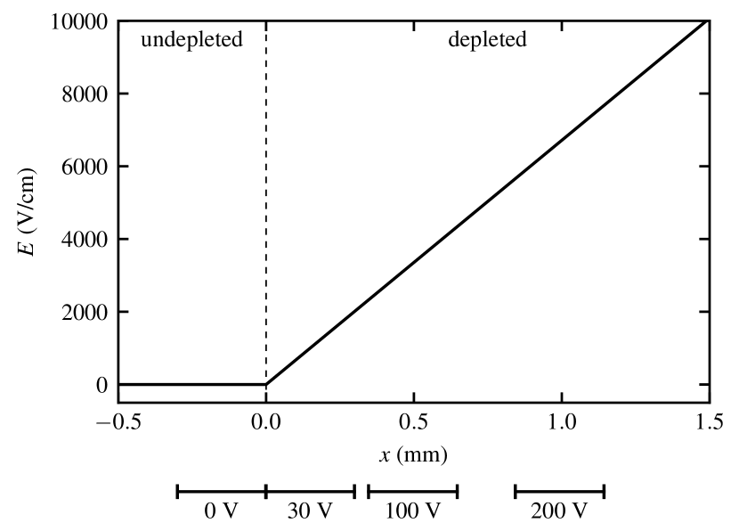
The transport equations are invariant with translation, so we’ll conveniently set the origin of axis at the interface between the depleted and undepleted regions, which could be real (inside) or virtual (outside the detector). This choice of coordinate system origin will greatly simplify accounting for offsets in subsequent sections. The resulting electric field is:
| (4) |
Fig. 2 shows the electric field dependence on position and illustrates detector coordinates for a few different bias voltages.
II-E Arbitrary Bias Voltage
With the origin at the interface between the undepleted and depleted regions, different biasing conditions result in different coordinates of the front and rear planes of the sensor (indicated in Fig. 2 for ).
The voltage drop over the sensor can be obtained by integrating Eq. 4 over (for simplicity we discard signs here); and are the positions of the front and back of the sensor, with . In a partially depleted sensor, thus . In a fully depleted sensor, the bias voltage is resulting in:
| (5) | |||
| (6) |
II-F Charge Generation, Transport and Recombination
Detecting individual quanta in semiconductors relies on the transient signals induced by charge transport (drift and diffusion), which in turn depends on charge generation at the interaction point(s) and recombination of carriers.
II-F1 Charge Generation
Different particles or photons generate distinct patterns that can be used to identify the detected particle. For example, visible and UV light photons generate single electron pairs. High fluxes are adequately described by existing steady state approximations.
X-ray photons generate discrete electron-hole clouds with thousands of carriers near the interaction point. Relativistic charged particles typically pass through the sensor in straight lines, depositing a constant amount of energy per length (Bethe formula). The signal can be integrated as a series of small signals over the track length. The steady state solution for x-ray photons and relativistic particles is trivial, and the transient signals have to be evaluated.
II-F2 Thermal Diffusion
II-F3 Charge Drift
Charge drift is determined by electric fields (accelerating charge carriers) and interactions with the lattice. At high field intensities, the average drift velocity asymptotically approaches the saturation velocity as the interactions with the lattice balance out the acceleration in the electric field. For , induces a carrier velocity component (drift velocity), which for indirect band gap semiconductors can be written as:
| (8) | |||
| (9) |
where is the saturation velocity. We call this a ”saturation velocity model”.
We introduce the and constants (Eq. 9), as they will be used extensively throughout this paper. For simplicity we will often use instead of . They are constant for each sensor (depending only on doping and, for minority carriers, also on mobility). Note that the forms in Eq. 9 are valid for n-type sensors (i.e., electrons are majority carriers and holes are minority carriers). The coefficients could be called ”linear velocity gradients”.
We show an example of drift velocity in Fig. 3 for minority carriers (holes, black lines) and majority carriers (electrons, red lines) in a typical sensor. Solid lines correspond to the saturation velocity model (Eq. 8) while dashed lines correspond to the linear velocity model (Eq. 10), demonstrating significant differences at bias voltages of in a typical sensor.
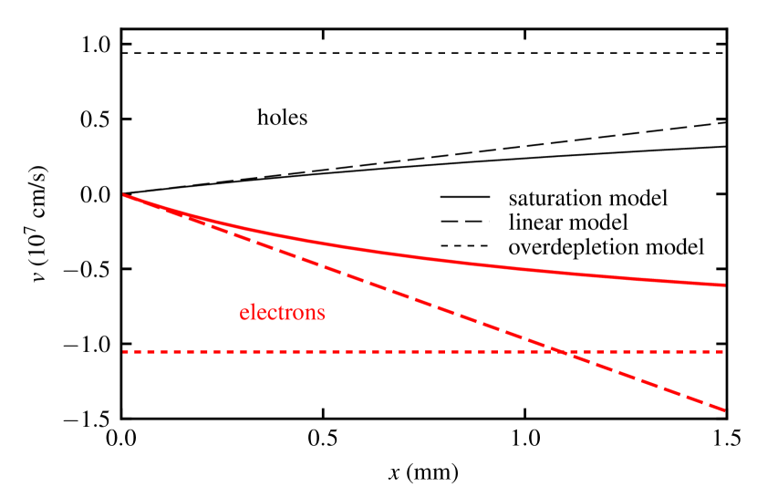
When ignoring the saturation effect of carrier velocity (), Eq. 8 is simplified to a ”linear velocity model”:
| (10) |
which is also appropriate for describing carrier drift in direct band gap semiconductors under the peak velocity.
If the sensor is overdepleted (i.e., ), the carrier velocity approaches the saturation velocity asymptotically:
| (11) |
further called ”overdepletion model”.
II-F4 Charge Recombination
Charge recombination typically has a time constant in the order of milliseconds [17], much larger than drift times (typically in the order of nanoseconds, Table III) and can usually be ignored. If this is not the case (e.g., after significant radiation damage [28]), the appropriate recombination rate can be used in the full form solutions (Eq. 13, 42).
II-G Partial Differential Equations
Solving the drift-diffusion-recombination partial differential equation yields the transient signals from single detected quanta. We solve and discuss the partial differential equations for minority carriers (i.e., holes in n-type sensors) as they induce most of the signal into the pixel readout. We will briefly mention the majority carriers and their solutions.
II-G1 General Equation
The hole density as a function of time and space can be written as . The effects of charge transport and recombination mechanisms can be summarized as:
| (12) |
where the right hand side terms correspond to thermal diffusion, drift in the electric field111The minus sign for the drift term in Eq. 12 is correct for positive equivalent to moving to the right., and charge recombination, respectively. A similar equation is valid for electron density .
While these two equations are coupled and electrostatic effects are present [29], in both the depleted and undepleted sensor the coupling is relatively weak. Electrostatic interactions become important when large signals are detected in a small volume and short time, resulting in ”plasma effects” [30].
II-G2 Field Along x Axis
The electric field components in the plane can usually be neglected222Close to the rear pixel contacts there are electric field components in-plane, however, their influence is relatively small as minority carriers drift relatively quickly through this region and are unlikely to diffuse to nearby pixels.. Usually the recombination rate does not depend on position and time, allowing us to extract the recombination term and multiply the solution with a factor instead. This allows separating the variables
| (13) |
and results in a 1D drift-diffusion equation (also called diffusion-advection) along the axis and diffusion in the plane. Thus we have to solve Eq. 12 only in one dimension for :
| (14) | |||
| (15) |
II-G3 Charge generation
For clarity, and in line with the prevailing notation (e.g., [26]), we will denote the initial conditions on , , and axes with , and . A discrete detection event at and location will generate a charge cloud:
| (16) |
Solving the carrier density equation for infinitely small initial distributions (i.e., functions) yields the Green’s function corresponding to the partial differential equation and initial and boundary conditions. For finite initial signals, the solution is a simple convolution of the Green’s function with the initial signal [26]. For , , , and are zero.
II-G4 Lateral Charge Diffusion
Assuming the sensor is very large in the plane and ignoring in-plane electric field components, charge drift as a function of time will be determined by:
| (17) | |||
| (18) |
with the familiar 2D diffusion solution:
| (19) |
III Overdepletion Velocity Model
III-A Green’s Function
With constant velocity (Eq. 11), this is essentially the diffusion model, drifting with constant velocity . The corresponding drift equation is:
| (20) |
and diffusion equation along (due to the absence of a velocity gradient, it reverts to simple thermal diffusion):
| (21) |
resulting in a relatively simple Green’s function for minority carriers:
| (22) |
IV Linear Velocity Model
In the linear velocity approximation we solve the partial differential equation (Eq. 14) with initial conditions Eq. 15 and (Eq. 10). At the boundaries, the recombination is instantaneous, thus and . Usually drift dominates diffusion at the boundaries so we can ignore the boundary conditions (see section V-E for a discussion on when this approximation is appropriate).
IV-A Drift
Single charge carriers drift and diffuse randomly. In localized clouds composed of many carriers, the drift of the center of the cloud will average out the stochastic diffusion of individual charge carriers, drifting from (inside the sensor) to in a time :
| (23) |
Solving for yields the charge cloud position :
| (24) |
The drift equation for majority carriers is obtained similarly:
| (25) |
IV-B Diffusion
In appendices A and B we present an approach to separate diffusion from drift (similar to the method of characteristics [26]), reducing the partial differential equation (Eq. 14) to an ordinary differential equation (Eq. 56) and obtaining the analytical solution for diffusion of minority carriers:
| (26) |
Note that (calculated using [31]) thus Eq. 26 is a generalized form of the simple diffusion equation (Eq. 7), incorporating the linear velocity gradient .
Similarly for majority carriers, the diffusion equation is:
| (27) |
IV-C Green’s Function
The Green’s function can be used to calculate for any initial condition through convolution over the initial conditions:
| (29) |
For initial condition (point source at and ), the integral above is reduced to the simple form:
| (30) |
IV-D Testing and Simulations
Substituting the Green’s function from Eq. 28 and drift velocity from Eq. 10 in the partial differential equation Eq. 14, calculating the partial derivatives and canceling identical terms demonstrates that Eq. 28 is the analytical solution.
To confirm the analytical results, we performed Monte Carlo simulations (tracking carriers in a typical sensor, with initial position ) and found that a time step yields stable results. We simulated a relatively long time () to prove the validity of the analytical solutions over wide ranges. The results of the numerical simulation are compared to the analytical functions in Fig. 4, showing a good fit between the analytical model and simulations.
However, the results are obviously nonphysical for large drift times and sensor thicknesses due to the exponential velocity increase implied by Eq. 24. We will account for the saturation velocity in a generalized saturation velocity model in section V, comparing the two models and discussing when to use each (section V-G).
V Saturation Velocity Model
With larger bias voltages , the saturation velocity is usually important, thus we’ll solve the partial differential equation Eq. 14 with initial conditions in Eq. 15 and the saturation velocity model in Eq. 8. As in section IV, we ignore the boundary conditions (see section V-E for a discussion on when this approximation is appropriate).
V-A Drift
Following the approach in section IV-A, the drift time for minority carriers from to is:
| (31) |
Solving for , we obtain the drift equation for minority carriers :
| (32) |
where is the Lambert W function. The drift time and drift equation for majority carriers are obtained similarly:
| (33) | |||
| (34) |
V-B Diffusion
Similarly to section IV-B, in appendices A and C we obtain an ordinary differential equation for diffusion (Eq. 61), resulting in the diffusion equation for minority carriers:
| (35) |
with given by Eq. 32. Note that depends on initial position . In the limit , this equation simplifies [31] to Eq. 26:
| (36) |
demonstrating that Eq. 35 is a further generalization of Eq. 26, incorporating the effects of velocity saturation.
Similarly for majority carriers (moving in the opposite direction), with given by Eq. 34:
| (37) |
V-C Green’s Function
V-D Simulations
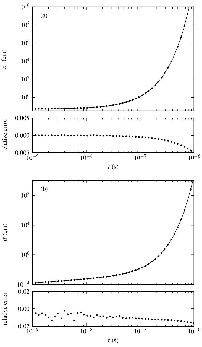
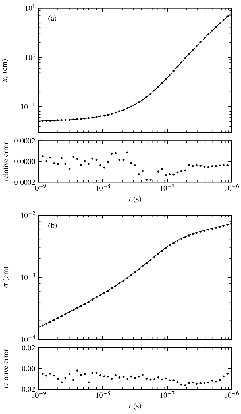
We performed Monte Carlo simulations as described in section IV-D. Numerical simulations confirm the charge cloud is close to a normal distribution (with negligible skewness and kurtosis), drifting along the axis. Fig. 5 shows the simulation results (dots) and analytical functions (lines) for both charge cloud position and size (along axis) , demonstrating good agreement between the analytical model and the simulations (relative error within and for the position and size, respectively). Other initial positions also result in a good match.
V-E Boundary Conditions
The Green’s function in Eq. 38 is valid for relatively large bias voltages where drift dominates diffusion at both the front and back planes. At low bias voltages, some charge is lost on recombination on the front surface. The charge loss fraction due to recombination on the front plane can be shown to be smaller than or equal to the least advantegeous case (small , large , carrier transport dominated by diffusion):
| (39) |
obtained by substituting from Eq. 28, which is appropriate for small .
For a detector with a signal to noise ratio of and a typical sensor, Eq. 28 and 38 can be used directly for an initial position with a charge loss fraction smaller than . For the typical sensor we obtain , which can be guaranteed with a depletion width , corresponding to a bias voltage (obtained using Eq. 3).
V-F Comparison with Overdepletion Model
The overdepletion approximation results in large errors for drift in a typical sensor, see summary in Table III, with errors up to a factor for a typical sensor. At bias in the typical sensor, the diffusion equation error is up to , as shown in Fig. 6 (b) and (c). This approximation is appropriate only for thin p-type sensors with high bias voltages.
| sensor | ||||
|---|---|---|---|---|
| n-type, | ||||
| n-type, | ||||
| n-type, | ||||
| p-type, | ||||
| p-type, | ||||
| p-type, | ||||
| n-type, | ||||
| n-type, | ||||
| n-type, | ||||
| p-type, | ||||
| p-type, | ||||
| p-type, | ||||
| is the drift time from the front to the back of the sensor (Eq. 31, 33); | ||||
| is calculated in the linear velocity model (Eq. 24, 25); | ||||
| is calculated in the overdepletion approximation as . | ||||
V-G Comparison with Linear Velocity Model
The saturation velocity model describes accurately the transient charge transfer in thick detectors or detectors with large bias voltages. To investigate the differences between the linear velocity model and the saturation velocity model, we calculated the drift and diffusion for a typical sensor, showing the results in Fig. 6.
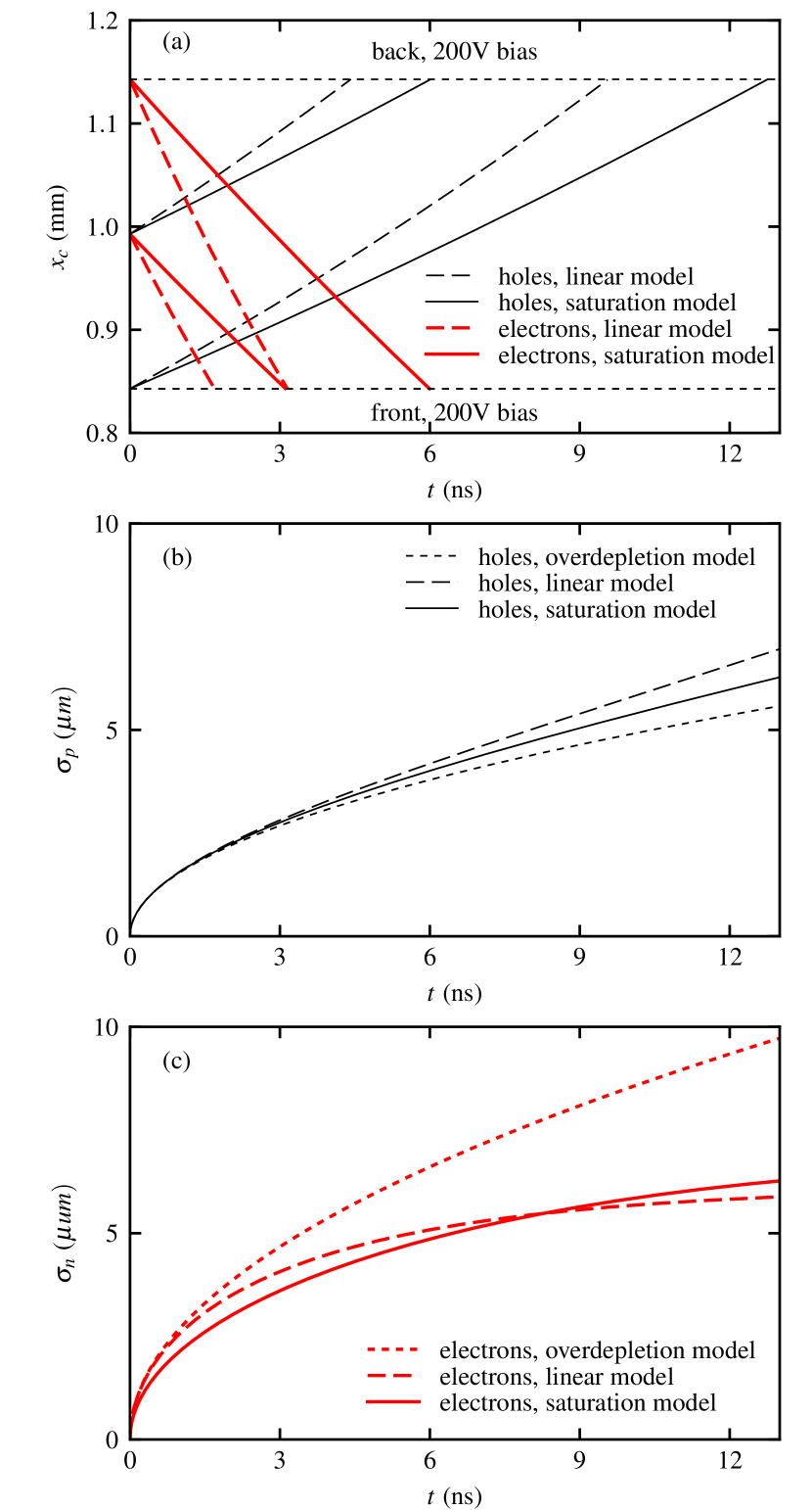
Both minority carriers (thin black lines) and majority carriers (thick red lines) were tracked through the detector volume, with a bias voltage . Three models were used: saturation drift and diffusion (solid lines), linear drift and diffusion (dashed lines) and simple diffusion ignoring the velocity gradients (dotted lines). We used three initial positions: on the front plane, middle of detector, and rear plane.
The three drift models diverge quickly, yielding differences in arrival times of up to for minority carriers and up to for majority carriers. The diffusion equations for minority carriers diverge more gradually, with similar results in the first nanoseconds. Only the linear and saturation diffusion equations for majority carriers are similar over a wide range of time (due to the thermal drift balancing the compressing velocity gradient).
Consequently, the saturation velocity model should always be used for indirect band gap semiconductors, unless a thin sensor with low bias is used. However, see section V-E for limitations associated with bias voltages close to the depletion voltage.
For direct band gap semiconductors (e.g., GaAs, CdTe), the carrier velocity profile as a function of the electric field increases more linearly up to a peak velocity at and then decreases asymptotically to a saturation velocity . In this case, the linear model should be used up to , and possibly extended piecewise with the overdepleted model for high electric fields.
VI Undepleted Sensor
In the case of undepleted sensors we must take into account the boundary conditions , and the charge recombination rate . We will assume that the sensor is depleted over at least a shallow width, to prevent high thermal noise. The partial differential equation Eq. 14 is reduced to a standard Dirichlet problem [26] with corresponding Green’s function expressed as an infinite sum:
| (40) |
Fig. 7 shows in a first approximation the response of a relatively thin () undepleted region of a partially depleted sensor (). A full model would account for the coupling at the depletion boundary () of the differential equations on the two domains. However, this model already allows us to draw some initial conclusions on the signals from the undepleted region. Fig. 7 (a) shows the evolution of the transient charge distribution ass a function of initial position .
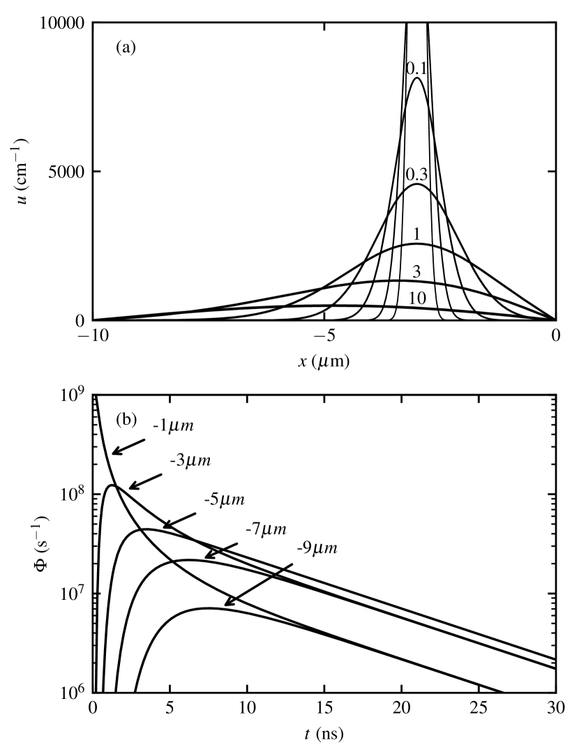
The carrier flux entering the readout ASIC is given by the left to right flux through boundary at time :
| (41) |
Fig. 7 (b) shows the coresponding transient charge flowing into the depleted region. For a relatively thin undepleted region, the minority carriers drift through the depletion boundary within tens of nanoseconds.
Total flux diffusing through boundary into the depleted region:
| (42) |
Note that the recombination rate is now tied up inside the summation terms. For low recombination rates :
| (43) |
reflecting charge loss through the front plane.
VII Applications
VII-A X-ray Photon Detection
VII-A1 Transient Charge Clouds
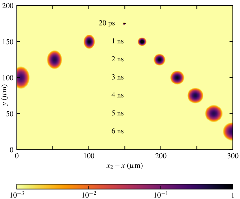
Using the Green’s function of the saturation velocity model (Eq. 32 and Eq. 35 inserted in Eq. 38), we calculate the transient carrier distribution, project it on the plane, and show the result in Fig. 8 for a typical sensor following a unit detection event in the middle of the sensor. The result is similar to Monte Carlo simulations, however, it is orders of magnitude faster.
VII-A2 Transient Current
The instantaneous current induced in one electrode due to the movement of one charge carrier is given by Ramo’s theorem [32] which requires taking into account the weighting potential [33]. Note that the weighting potential is unrelated to the biasing or doping of the detector and can not be solved analytically in pixel detectors [34]. In pixel sensors the weighting potential decreases quickly away from a pixel readout pad, thus we can assume in a first approximation that the weighting field is everywhere except on the current pixel readout pad, where .
The expected current (in the statistical sense, as average of currents of many single carriers) for a single charge carrier through a boundary can be calculated easily from (Eq. 38):
| (44) |
A typical detection event generates hundreds or thousands of carrier pairs, with currents approaching asymptotically the distribution shown in Eq. 44, multiplied by the number of carriers. The current density resulting from carriers is:
| (45) |
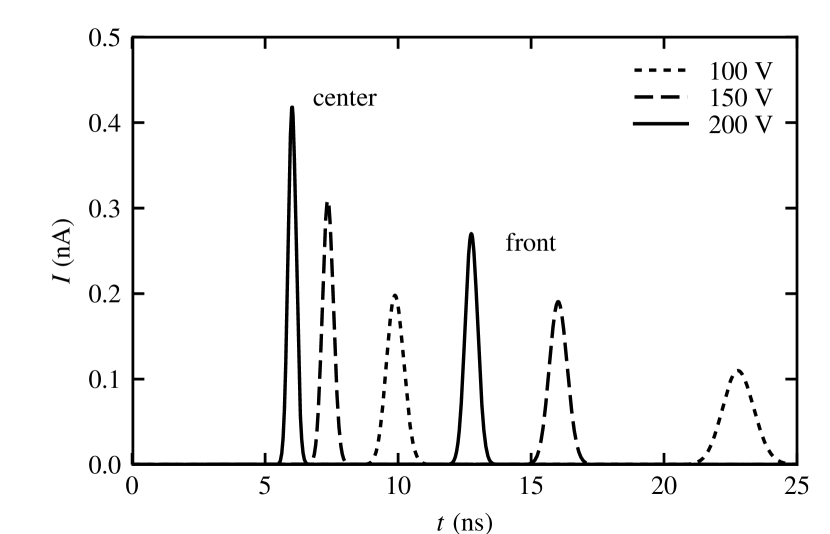
In Fig. 9 we show the current from a single carrier in a typical sensor with initial position either at the front or in the middle of the sensor for 3 biasing conditions (, and ). The drift time increases rapidly with lower bias and initial position closer to the sensor front plane.
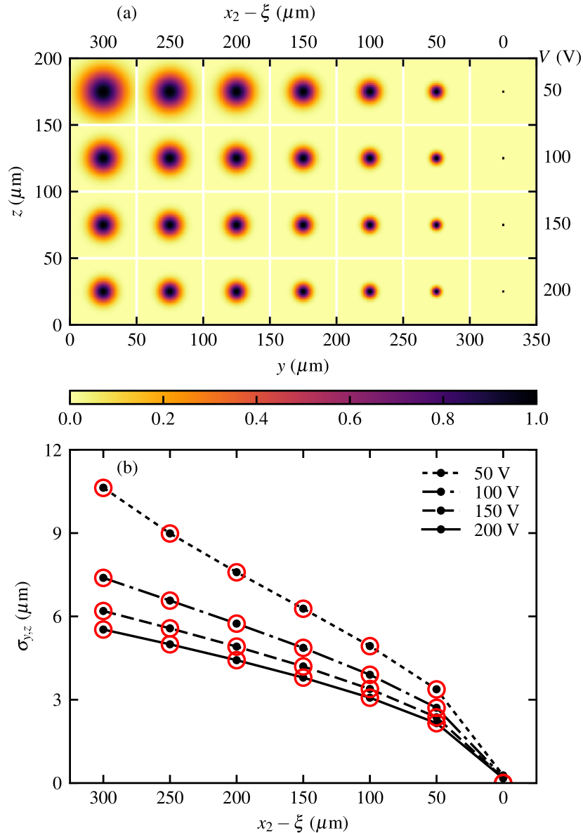
VII-A3 Charge Cloud Size and Charge Sharing
Assuming a square pixel in the plane with pitch and center at collecting charge from a single carrier with initial position , the current entering the pixel at time is obtained by integrating between the pixel boundaries, resulting in:
| (46) |
Eq. 46 can be easily and efficiently extended to 2D pixel arrays.
The total charge collected in a pixel can be calculated by integrating Eq. 46 numerically:
| (47) |
In Fig. 10, black dots indicate results of the numerical integration (Eq. 46, 47) for the typical sensor and a range of initial positions and biasing conditions.
VII-B Relativistic Charged Particle Detection
VII-B1 Charge Cloud Size
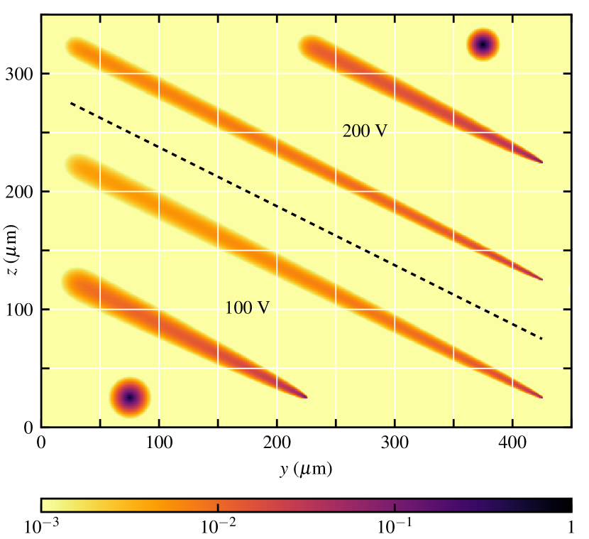
In Fig. 11 we show charge sharing profiles for relativistic electron tracks for two different bias settings ( and ) and three different incidence angles (, and ). For an application in tracking relativistic electron beams see [35].
VIII Conclusion
We present for the first time analytical solutions for fast and accurate calculation of transient carrier densities in p-n junction sensors by solving the drift-diffusion-recombination equations for the minority and majority carriers in a variety of conditions: undepleted, depleted with linear velocity (carrier velocity proportional to electric field), depleted with saturation velocity (carrier velocity transitioning from proportional to electric field to velocity saturation), and overdepleted (carriers moving with saturation velocity). We also show that the diffusion equations in the linear velocity model and in the saturation velocity model are increasingly generalized forms of the simple diffusion equation. We subsequently obtain the corresponding Green’s functions which allow describing any initial conditions with a simple convolution.
Previously, analytical solutions were only available for simple diffusion (in the absence of drift velocity gradients). In practice, drift-diffusion is often simulated numerically with Monte Carlo simulations, finite elements simulations (including TCAD tools), or simple assumptions. Comparing our analytical drift-diffusion solutions with Monte Carlo simulations and TCAD simulations (using industry standard Synopsys Sentaurus) shows good agreement.
We deduce equations for the transient behaviour of (1) charge clouds resulting from detection of x-ray and gamma-ray photons at different depths and (2) detection of relativistic charged particles and resulting tracks. We illustrate the results for a typical silicon sensor (n-type, thick, resistivity), however, the analytical equations can be extended to any reverse-biased p-n junction pixel or strip sensor.
The transient charge cloud evolution can be used to describe the behaviour of timing pixel detectors. In particular, ”time of arrival” and ”time over threshold” measurements (defined as time until the transient signal exceeds a set threshold, and time elapsed until the transient signal returns under the set threshold) depend on threshold setting, photon energy, bias voltage, pixel geometry, 3D detection position (with subpixel accuracy); see holistic approaches to model these effects in Timepix for photons [36], pions [37], protons and carbon ions [38]. Timepix3 [9] and tPix [10] have increasing ”time of arrival” resolutions of and , respectively.
Appropriate integration of the transient signals provides an accurate description of charge sharing for any pixel or strip detector for different conditions (interaction positions, track orientations, subpixel position, bias voltage, and pixel geometry) for photons and relativistic charged particle tracks. This can be used in extracting the 3D+T (x,y,z,time) of photon interactions (with subpixel resolution and accurate depth information) as well as the 4D+T (x,y,\texttheta,\textphi) track equation for relativistic charged particles.
Appendix A Diffusion in Gradient Fields
To separate diffusion from drift, we introduce a coordinate system change from to the position on the characteristic curve [39]:
| (48) |
For a normal distribution, positions correspond to locations which separate fractions of the charge carriers (i.e., where ). In this coordinate system, the evolution of the average standard deviation of the charge cloud is described by:
| (49) |
where is a function of :
| (50) |
with the definition of above, diffusion leads to:
| (51) |
and is identical with its position in coordinate :
| (52) |
We can also estimate:
| (53) |
Appendix B Diffusion in Linear Velocity Model
With :
| (55) |
and substituting in Eq. 54 results in an ordinary differential equation:
| (56) |
with solution [31]:
| (57) |
leading, with Eq. 24, to a Green’s function:
| (58) |
which is an analytical solution for the partial differential equation. Note that the same result can be obtained [40] by substituting and showing that Eq. 14 is reduced to an ordinary differential equation which is straightforward to solve and yields the same solution.
Appendix C Diffusion with Saturation Velocity
We can expand Eq. 53 in Taylor series:
| (59) |
Substituting the actual saturation velocity formula (Eq. 8), noting that thus , and keeping only the first term, after some cancellation:
| (60) |
which results in an ordinary differential equation for diffusion:
| (61) |
Acknowledgment
Use of the Linac Coherent Light Source (LCLS), SLAC National Accelerator Laboratory, is supported by the U.S. Department of Energy, Office of Science, Office of Basic Energy Sciences under Contract No. DE-AC02-76SF00515.
The authors are grateful to C. Genes (Max Plank Institute for the Science of Light, Erlangen, Germany) and A. Dragone, C. Stan and C.-E. Chang (SLAC National Accelerator Laboratory, Menlo Park, California) for many stimulating discussions.
We applied the SDC approach for the sequence of authors [41]. Statement of authorship: conception, G. Blaj; analytical methods, G. Blaj; simulations, G. Blaj and J. Segal; drafting the manuscript, G. Blaj; revising the manuscript: all authors.
References
- [1] P. Delpierre, “A history of hybrid pixel detectors, from high energy physics to medical imaging,” Journal of Instrumentation, vol. 9, no. 05, p. C05059, 2014. [Online]. Available: https://doi.org/10.1088/1748-0221/9/05/C05059
- [2] M. Campbell, E. Heijne, G. Meddeler, E. Pernigotti, and W. Snoeys, “A readout chip for a 64 x 64 pixel matrix with 15-bit single photon counting,” IEEE Transactions on Nuclear Science, vol. 45, no. 3, pp. 751–753, 1998. [Online]. Available: https://doi.org/10.1109/23.682629
- [3] X. Llopart, M. Campbell, D. San Segundo, E. Pernigotti, and R. Dinapoli, “Medipix2, a 64k pixel read out chip with 55 m square elements working in single photon counting mode,” in Nuclear Science Symposium Conference Record, 2001 IEEE, vol. 3. IEEE, 2001, pp. 1484–1488. [Online]. Available: https://doi.org/10.1109/23.682629
- [4] C. Broennimann, E. Eikenberry, B. Henrich, R. Horisberger, G. Huelsen, E. Pohl, B. Schmitt, C. Schulze-Briese, M. Suzuki, T. Tomizaki et al., “The Pilatus 1M detector,” Journal of Synchrotron Radiation, vol. 13, no. 2, pp. 120–130, 2006. [Online]. Available: https://doi.org/10.1107/S0909049505038665
- [5] G. Blaj, P. Caragiulo, A. Dragone, G. Haller, J. Hasi, C. J. Kenney, M. Kwiatkowski, B. Markovic, J. Segal, and A. Tomada, “X-ray imaging with ePix100a, a high-speed, high-resolution, low-noise camera,” SPIE Proceedings, vol. 9968, pp. 99 680J–99 680J–10, June 2016. [Online]. Available: https://dx.doi.org/10.1117/12.2238136
- [6] R. Ballabriga, J. Alozy, G. Blaj, M. Campbell, M. Fiederle, E. Frojdh, E. H. M. Heijne, X. Llopart, M. Pichotka, S. Procz et al., “The Medipix3RX: a high resolution, zero dead-time pixel detector readout chip allowing spectroscopic imaging,” Journal of Instrumentation, vol. 8, no. 02, p. C02016, 2013. [Online]. Available: https://dx.doi.org/10.1088/1748-0221/8/02/C02016
- [7] A. Dragone, P. Caragiulo, B. Markovic, G. Blaj, J. Hasi, J. Segal, A. Tomada, K. Nishimura, R. Herbst, P. Hart, S. Osier, J. Pines, C. J. Kenney, and G. Haller, “ePixS: a high channel count x-ray spectroscopy detector for x-ray FELs,” 2015, talk presented at the IEEE Nuclear Science Symposium and Medical Imaging Conference (NSS/MIC), San Diego, CA. Nov 2015.
- [8] X. Llopart, R. Ballabriga, M. Campbell, L. Tlustos, and W. Wong, “Timepix, a 65k programmable pixel readout chip for arrival time, energy and/or photon counting measurements,” Nuclear Instruments and Methods in Physics Research Section A: Accelerators, Spectrometers, Detectors and Associated Equipment, vol. 581, no. 1–2, pp. 485 – 494, 2007, proceedings of the 11th International Vienna Conference on Instrumentation. [Online]. Available: https://dx.doi.org/10.1016/j.nima.2007.08.079
- [9] T. Poikela, J. Plosila, T. Westerlund, M. Campbell, M. De Gaspari, X. Llopart, V. Gromov, R. Kluit, M. van Beuzekom, F. Zappon et al., “Timepix3: a 65k channel hybrid pixel readout chip with simultaneous toa/tot and sparse readout,” Journal of instrumentation, vol. 9, no. 05, p. C05013, 2014. [Online]. Available: https://doi.org/10.1088/1748-0221/9/05/C05013
- [10] B. Markovic, P. Caragiulo, A. Dragone, C. Tamma, T. Osipov, C. Bostedt, M. Kwiatkowski, J. Segal, J. Hasi, G. Blaj, C. J. Kenney, and G. Haller, “Design and characterization of the tPix prototype: a spatial and time resolving front-end ASIC for electron and ion spectroscopy experiments at LCLS,” in 2016 IEEE Nuclear Science Symposium and Medical Imaging Conference (NSS/MIC). IEEE, 2016, in press.
- [11] D. Greiffenberg, “The AGIPD detector for the European XFEL,” Journal of Instrumentation, vol. 7, no. 01, p. C01103, 2012. [Online]. Available: https://dx.doi.org/10.1088/1748-0221/7/01/C01103
- [12] P. Caragiulo, A. Dragone, B. Markovic, R. Herbst, K. Nishimura, B. Reese, S. Herrmann, P. Hart, G. Blaj, J. Segal, A. Tomada, J. Hasi, G. Carini, C. J. Kenney, and G. Haller, “Design and characterization of the ePix10k prototype: A high dynamic range integrating pixel ASIC for LCLS detectors,” in 2014 IEEE Nuclear Science Symposium and Medical Imaging Conference (NSS/MIC). IEEE, Nov 2014, pp. 1–3. [Online]. Available: https://dx.doi.org/10.1109/NSSMIC.2014.7431049
- [13] F. Erdinger, L. Bombelli, D. Comotti, S. Facchinetti, P. Fischer, K. Hansen, P. Kalavakuru, M. Kirchgessner, M. Manghisoni, M. Porro et al., “The DSSC pixel readout ASIC with amplitude digitization and local storage for DEPFET sensor matrices at the European XFEL,” in Nuclear Science Symposium and Medical Imaging Conference (NSS/MIC), 2012 IEEE. IEEE, 2012, pp. 591–596. [Online]. Available: https://dx.doi.org/10.1109/NSSMIC.2012.6551176
- [14] H. T. Philipp, M. W. Tate, P. Purohit, D. Chamberlain, K. S. Shanks, J. T. Weiss, S. M. Gruner, Q. Shen, and C. Nelson, “High-speed x-ray imaging with the Keck pixel array detector (Keck PAD) for time-resolved experiments at synchrotron sources,” in AIP Conference Proceedings, vol. 1741. AIP Publishing, 2016, p. 040036. [Online]. Available: https://dx.doi.org/10.1063/1.4952908
- [15] G.-F. Dalla Betta, “Why and how pixels are becoming more and more intelligent (sensors-part 2),” Journal of Instrumentation, vol. 10, no. 07, p. C07010, 2015. [Online]. Available: https://doi.org/10.1088/1748-0221/10/07/C07010
- [16] G. Lutz, Semiconductor radiation detectors. Springer Berlin Heidelberg, 1999, 2007. [Online]. Available: https://dx.doi/org/doi:10.1007/978-3-540-71679-2
- [17] B. van Zeghbroeck, Principles of Semiconductor Devices. Boulder, Colorado: B. van Zeghbroeck, 2011. [Online]. Available: https://ecee.colorado.edu/ bart/book/book/title.htm
- [18] J. D. Plummer, M. D. Deal, and P. B. Griffin, Silicon VLSI Technology: Fundamentals, Practice, and Modeling, 1st ed. Upper Saddle River, New Jersey: Prentice Hall, 2000.
- [19] R. W. Dutton and A. J. Strojwas, “Perspectives on technology and technology-driven CAD,” IEEE Transactions on Computer-Aided Design of Integrated Circuits and Systems, vol. 19, no. 12, pp. 1544–1560, 2000. [Online]. Available: https://doi.org/10.1109/43.898831
- [20] A. Bortolossi, “3D finite element drift diffusion simulation of semiconductor devices,” Master’s thesis, Politecnico di Milano, Milan, Italy, 2014. [Online]. Available: http://hdl.handle.net/10589/94468
- [21] F. Cenna, N. Cartiglia, M. Friedl, B. Kolbinger, H.-W. Sadrozinski, A. Seiden, A. Zatserklyaniy, and A. Zatserklyaniy, “Weightfield2: A fast simulator for silicon and diamond solid state detector,” Nuclear Instruments and Methods in Physics Research Section A: Accelerators, Spectrometers, Detectors and Associated Equipment, vol. 796, pp. 149–153, 2015. [Online]. Available: https://doi.org/10.1016/j.nima.2015.04.015
- [22] G. Potdevin, U. Trunk, and H. Graafsma, “HORUS, an HPAD x-ray detector simulation program,” Journal of Instrumentation, vol. 4, no. 09, p. P09010, 2009. [Online]. Available: https://dx.doi.org/10.1088/1748-0221/4/09/P09010
- [23] J. Becker, E. Fretwurst, and R. Klanner, “Measurements of charge carrier mobilities and drift velocity saturation in bulk silicon of <111> and <100> crystal orientation at high electric fields,” Solid-State Electronics, vol. 56, no. 1, pp. 104–110, 2011. [Online]. Available: https://dx.doi.org/10.1016/j.sse.2010.10.009
- [24] Synopsis, “Sentaurus,” Mountain View, California, 2016, version 2016.12.
- [25] S. M. Sze and K. K. Ng, Physics of semiconductor devices, 3rd ed. Hoboken, New Jersey: John Wiley & Sons, 2006.
- [26] J. D. Logan, Applied partial differential equations, 3rd ed. New York, New York: Springer, 2014. [Online]. Available: https://doi.org/10.1007/978-3-319-12493-3
- [27] A. Einstein, “Über die von der molekularkinetischen theorie der wärme geforderte bewegung von in ruhenden flüssigkeiten suspendierten teilchen,” Annalen der Physik, vol. 322, no. 8, pp. 549–560, 1905. [Online]. Available: https://doi.org/10.1002/andp.19053220806
- [28] J. J. Loferski and P. Rappaport, “Radiation damage in Ge and Si detected by carrier lifetime changes: Damage thresholds,” Phys. Rev., vol. 111, pp. 432–439, Jul 1958. [Online]. Available: https://doi.org/10.1103/PhysRev.111.432
- [29] J. Segal, J. Plummer, and C. Kenney, “Simulation of charge cloud evolution in silicon drift detectors,” in Nuclear Science Symposium, 1996. Conference Record., 1996 IEEE, vol. 1. IEEE, 1996, pp. 558–562. [Online]. Available: https://doi.org/10.1109/NSSMIC.1996.591061
- [30] J. Becker, K. Gärtner, R. Klanner, and R. Richter, “Simulation and experimental study of plasma effects in planar silicon sensors,” Nuclear Instruments and Methods in Physics Research Section A: Accelerators, Spectrometers, Detectors and Associated Equipment, vol. 624, no. 3, pp. 716–727, 2010. [Online]. Available: https://doi.org/10.1016/j.nima.2010.10.010
- [31] Wolfram Research, “Mathematica,” Champaign, Illinois, 2017, version 11.1.
- [32] S. Ramo, “Currents induced by electron motion,” Proceedings of the IRE, vol. 27, no. 9, pp. 584–585, 1939. [Online]. Available: https://doi.org/10.1109/JRPROC.1939.228757
- [33] W. Riegler, “Electric fields, weighting fields, signals and charge diffusion in detectors including resistive materials,” Journal of Instrumentation, vol. 11, no. 11, p. P11002, 2016. [Online]. Available: https://doi.org/doi:10.1088/1748-0221/11/11/P11002
- [34] W. Riegler and G. A. Rinella, “Point charge potential and weighting field of a pixel or pad in a plane condenser,” Nuclear Instruments and Methods in Physics Research Section A: Accelerators, Spectrometers, Detectors and Associated Equipment, vol. 767, pp. 267–270, 2014. [Online]. Available: https://doi.org/10.1016/j.nima.2014.08.044
- [35] G. Blaj, C. J. Kenney, P. Caragiulo, A. Dragone, G. Haller, P. Hansson, C. Hast, R. Herbst, B. Markovic, and T. Smith, “3D electron tracking and vertexing with single plane pixel detectors,” in 2016 IEEE Nuclear Science Symposium and Medical Imaging Conference (NSS/MIC). IEEE, 2016, in press.
- [36] J. Jakubek, “Precise energy calibration of pixel detector working in time-over-threshold mode,” Nuclear Instruments and Methods in Physics Research Section A: Accelerators, Spectrometers, Detectors and Associated Equipment, vol. 633, pp. S262–S266, 2011. [Online]. Available: https://doi.org/10.1016/j.nima.2010.06.183
- [37] K. Akiba, M. Artuso, R. Badman, A. Borgia, R. Bates, F. Bayer, M. van Beuzekom, J. Buytaert, E. Cabruja, M. Campbell et al., “Charged particle tracking with the Timepix ASIC,” Nuclear Instruments and Methods in Physics Research Section A: Accelerators, Spectrometers, Detectors and Associated Equipment, vol. 661, pp. 31–49, 2012. [Online]. Available: https://doi.org/10.1016/j.nima.2011.09.021
- [38] B. Hartmann, P. Soukup, C. Granja, J. Jakubek, S. Pospíšil, O. Jäkel, and M. Martišíková, “Distortion of the per-pixel signal in the Timepix detector observed in high energy carbon ion beams,” Journal of Instrumentation, vol. 9, no. 09, p. P09006, 2014. [Online]. Available: https://doi.org/10.1088/1748-0221/9/09/P09006
- [39] J. D. Logan, An introduction to nonlinear partial differential equations, 2nd ed. Hoboken, New Jersey: John Wiley & Sons, 2008.
- [40] A. D. Polyanin and V. F. Zaitsev, Handbook of nonlinear partial differential equations. Boca Raton, Florida: Chapman and Hall/CRC, 2004.
- [41] T. Tscharntke, M. E. Hochberg, T. A. Rand, V. H. Resh, and J. Krauss, “Author sequence and credit for contributions in multiauthored publications,” PLoS Biol, vol. 5, no. 1, p. e18, 2007. [Online]. Available: https://doi.org/10.1371/journal.pbio.0050018