Nonmonotonic strain dependence of lattice thermal conductivity in monolayer SiC: a first-principles study
Abstract
An increasing number of two-dimensional (2D) materials have already been achieved experimentally or predicted theoretically, which have potential applications in nano- and opto-electronics. Various applications for electronic devices are closely related to their thermal transport properties. In this work, the strain dependence of phonon transport in monolayer SiC with a perfect planar hexagonal honeycomb structure is investigated by solving the linearized phonon Boltzmann equation. It is found that room-temperature lattice thermal conductivity () of monolayer SiC is two orders of magnitude lower than that of graphene. The low is due to small group velocities and short phonon lifetimes, which can also be explained by polarized covalent bond due to large charge transfer from Si to C atoms. In considered strain range, it is proved that the SiC monolayer is mechanically and dynamically stable. With increased tensile strain, the of SiC monolayer shows an unusual nonmonotonic up-and-down behavior, which is due to the competition between the change of phonon group velocities and phonon lifetimes of low frequency phonon modes. At low strains (8%), the phonon lifetimes enhancement induces the increased , while at high strains (8%) the reduction of group velocities as well as the decrease of the phonon lifetimes are the major mechanism responsible for decreased . Our works further enrich studies on phonon transports of 2D materials with a perfect planar hexagonal honeycomb structure, and motivate farther experimental studies.
pacs:
72.15.Jf, 71.20.-b, 71.70.Ej, 79.10.-n Email:guosd@cumt.edu.cnI Introduction
Due to their fascinating physical and chemical properties, 2D materials have attracted increasing attention since the successful synthesis of grapheneq1 . In comparison with the gapless graphene, semiconducting transition-metal dichalcogenide (TMD)q7 , group IV-VIq8 , group-VAq9 ; q10 , group-IVq11 , GaNq12 and ZnOq13 monolayers have intrinsic energy band gaps. Thermal management is very important for next generation of electronics and optoelectronic devices based on these 2D materialsq14 , which has been hot spot in the field of materials. The thermal transports of many 2D materials have been studied from a combination of first-principles calculations and the linearized phonon Boltzmann equationq15 ; q16 ; q17 ; p5 ; p5-1 ; p5-2 . The phonon transports of 2D orthorhombic group IV-VI compounds (GeS, GeSe, SnS and SnSe) have been systematically investigated, and they show diverse anisotropic properties along the zigzag and armchair directionsq15 . Phonon transport properties of 2D group-IV materials have been performed, and although the decreases monotonically from graphene to silicene to germanene, unexpected higher is observed in staneneq16 . The thermal transports of group-VA elements (As, Sb, Bi) monolayers with graphenelike buckled structure have been studied, including both electron and phonon partsq17 . The phonon transports of TMD (M=Mo, W, Zr and Hf; X=S and Se) monolayers have been systematically investigatedp5 . The of 2H-type TMD monolayers are generally higher than those of 1T-type ones due to the larger acoustic-optical frequency gapp5 . Strain effects on have also been carried out in various kinds of 2D materials, such Sb and AsP monolayerq18 ; q18-1 , 2D group-IVq19 , 2D q19-1 and 2D penta-structures materialsq20 . The shows diverse strain dependence, such as monotonously increasing, up-and-down and monotonously decreasing behaviors with increasing strain.
Like graphene, ZnO and GaN monolayers possess a perfect planar hexagonal honeycomb structural configuration, and their have been investigated from a first-principles studyq21 ; q22 . The room-temperature of monolayer ZnO is 4.5 with the thickness of 3.04 , and it’s lattice thermal conductivity shows anomalous temperature dependenceq21 . The of monolayer GaN (300 K) is 14.93 with the thickness of 3.74 , and the low can be explained by the special orbital hybridization mediated by the Ga- orbitalq22 . Recently, atomic resolution scanning transmission electron microscopy observations provide direct experimental indication of a two-dimensional form of silicon carbide, and the ground state of 2D SiC is indeed completely planar by extensive simulationsq23 . Similar to ZnO and GaN monolayers, 2D-SiC adopts a perfect planar hexagonal honeycomb structure with the gap of 2.58 eV using GGA.
In this work, strain-dependent phonon transport properties of SiC monolayer are studied by solving the linearized phonon Boltzmann equation based on first-principles calculations. The calculated room-temperature sheet thermal conductance of SiC monolayer is 301.66 , which is substantially lower than that of graphene (about 12884 )2dl . The mode level phonon group velocities and phonon lifetimes are used to investigate the mechanism underlying the lower of monolayer SiC compared with graphene. The strongly polarized Si-C bond, caused by large charge transfer between Si and C atoms, induces large phonon anharmonicity, and gives rise to the intrinsic low of monolayer SiC. As the strain increases, the of SiC monolayer shows a nonmonotonic up-and-down behavior, which can be understood by the competition between the change of phonon group velocities and phonon lifetimes of low frequency phonon modes.
The rest of the paper is organized as follows. In the next section, we shall give our computational details about phonon transport. In the third section, we shall present strain-dependent phonon transport of monolayer SiC. Finally, we shall give our conclusions in the fourth section.
II Computational detail
First-principles calculations are carried out using the projected augmented wave (PAW) method, and the exchange-correlation functional of generalized gradient approximation of the Perdew-Burke-Ernzerhof (GGA-PBE) is adopted, as implemented in the VASP codepv1 ; pv2 ; pbe ; pv3 . A plane-wave basis set is employed with kinetic energy cutoff of 700 eV, and the () and () orbitals of C(Si) atoms are treated as valance ones. The unit cell of monolayer SiC is built with the vacuum region of larger than 17 to avoid spurious interaction. The electronic stopping criterion is eV. The of monolayer SiC is calculated by solving linearized phonon Boltzmann equation with the single mode relaxation time approximation (RTA), as implemented in the Phono3py codepv4 . The can be expressed as:
| (1) |
where , and are phonon mode, the total number of q points sampling Brillouin zone (BZ) and the volume of a unit cell, and , , is the specific heat, phonon velocity, phonon lifetime. The phonon lifetime can be attained by phonon linewidth of the phonon mode :
| (2) |
The takes the form analogous to the Fermi golden rule:
| (3) |
in which and are the phonon equilibrium occupancy and the strength of interaction among the three phonons , , and involved in the scattering.
The interatomic force constants (IFCs) are calculated by the finite displacement method. The second-order harmonic IFCs are calculated using a 5 5 1 supercell containing 50 atoms with k-point meshes of 3 3 1. Using the harmonic IFCs, phonon dispersion of monolayer SiC can be attained, as implemented in Phonopy packagepv5 . The phonon dispersion determines the allowed three-phonon scattering processes, and further the group velocity and specific heat can be attained. The third-order anharmonic IFCs are calculated using a 4 4 1 supercells containing 32 atoms with k-point meshes of 4 4 1. Based on third-order anharmonic IFCs, the three-phonon scattering rate can be calculated, and further the phonon lifetimes can be attained. To compute , the reciprocal spaces of the primitive cells are sampled using the 120 120 1 meshes.
For 2D material, the calculated depends on the length of unit cell along z direction2dl . The should be normalized by multiplying , in which is the length of unit cell along z direction and is the thickness of 2D material, but the d is not well defined. In this work, the length of unit cell (18 ) along z direction is used as the thickness of monolayer SiC. To make a fair comparison between various 2D monolayers, the thermal sheet conductance can be used, defined as .
III MAIN CALCULATED RESULTS AND ANALYSIS
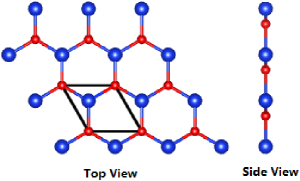
Like graphene, monolayer ZnO and monolayer GaN, monolayer SiC possesses a perfect planar hexagonal honeycomb structureq23 , which can be constructed by substituting one C atom in the unit cell of graphene with Si atom. The space symmetry group is for monolayer SiC, being lower than that of graphene (), which is because monolayer SiC contains two kinds of atoms in the unit cell. The schematic crystal structure is shown in Figure 1, and the optimized lattice parameter is 3.104 . It is worth noting that the bulk SiC possesses buckled structure for SiC layer, being different from planar structure for monolayer SiC, which may be due to the variation of orbital hybridization from to .
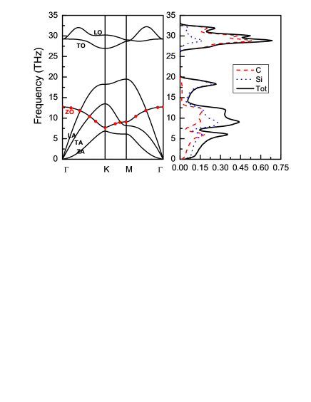
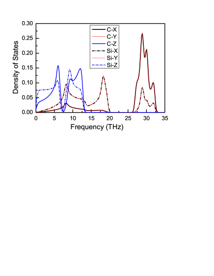
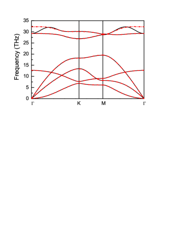
Based on the harmonic IFCs, the phonon dispersion of monolayer SiC is obtained along high-symmetry path, which along with total and partial density of states (DOS) are plotted in Figure 2. The phonon dispersion gives no imaginary frequencies, which indicates the thermodynamic stability of monolayer SiC. Due to two atoms per unit cell, the phonon dispersion of monolayer SiC includes 3 acoustic and 3 optical phonon branches. The two highest phonon branches are the in-plane transverse optical (TO) and the in-plane longitudinal optical (LO) branches. It is clearly seen that there is a phonon band gap of 7.47 THz, separating TO and LO branches from out-of-plane optical (ZO), in-plane longitudinal acoustic (LA), in-plane transverse acoustic (TA) and out-of-plane acoustic (ZA) branches. The phonon band gap may be caused by different atomic masses of C and Si atoms. Based on the highest acoustic frequency, the Debye temperature can be attained by , where is the Planck constant, and is the Boltzmann constant. The calculated value is about 935 K, which is lower than that of graphene (1977 K)q22 . The ZO branch crosses with the TA and LA branches, and there is a phonon band gap of 0.89 THz between ZA and ZO branches. Similar crosses can also be found in ZnO and GaN monolayersq21 ; q22 , but a phonon band gap is absent between ZA and ZO branches for monolayer GaN. The TA and LA branches are linear near the point, while the ZA branch deviates from linearity near the point, which can be found in many 2D materialsq15 ; q16 ; q17 ; q21 ; q22 . The partial DOS indicates that TO and LO branches are mainly contributed by the vibrations of C atoms. According to Figure 3, TA and LA branches are mainly from Si vibrations, while ZA and ZO branches are contributed by the vibrations of C and Si atoms.

| Direction | (C) | (Si) | |
|---|---|---|---|
| -3.674 | 3.674 | 2.531 | |
| -3.674 | 3.674 | 2.531 | |
| -0.271 | 0.271 | 1.180 |
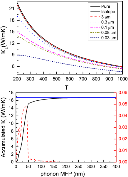
The intrinsic of monolayer SiC is calculated by solving the linearized phonon Boltzmann equation within single-mode RTA method. The phonon-isotope scattering is calculated based on the formula proposed by Shin-ichiro Tamuraq24 . For boundary scattering, is just used as the scattering rate, where is the group velocity and is the boundary mean free path (MFP). The lattice thermal conductivities of infinite (Pure and Isotope) and finite-size (3, 0.3, 0.1, 0.08 and 0.03 ) monolayer SiC as a function of temperature are plotted in Figure 4. The room-temperature of infinite (Pure) monolayer SiC is 16.76 with the thickness of 18 , and the corresponding thermal sheet conductance is 301.66 , which is two orders of magnitude lower than that for graphene (about 12884 )2dl . It is clearly seen that the isotope scattering has little effect on the lattice thermal conductivity of monolayer SiC, which may be due to the strong phonon-phonon scattering. With the sample size decreasing, the lattice thermal conductivity decreases due to enhanced boundary scattering. For the 3 and 0.3 cases, the change is very small with respect to infinite case. The for the 0.03 case is reduced to about half of that for infinite case at room temperature. To further understand the size dependence, the cumulative along with the derivatives with respect to MFP (300 K) are plotted in Figure 4. With MFP increasing, the cumulative approaches maximum. Phonons with MFP larger than 0.15 have very little contribution to the . Phonons with MFP smaller than 0.03 contribute around 50% to the .
To understand deeply phonon transport of monolayer SiC, the mode level phonon group velocities and lifetimes are shown in Figure 5. The largest group velocity for TA and LA branches near point is 8.74 and 14.80 , which are lower than those of grapheneq22 . Moreover, the overall phonon group velocities of monolayer SiC are smaller than those of graphene, which partially leads to lower for monolayer SiC than graphene. The phonon lifetimes can be calculated from three-phonon scattering rate by third-order anharmonic IFCs. It is found that ZA branch has relatively large phonon lifetimes. Due to the reflectional symmetry of monolayer SiC, the scattering channels involving odd numbers of ZA modes are largely suppressed, which leads to the low scattering rate of ZA, and then induces large phonon lifetimes. The lifetimes of TO and LO phonon branches are much larger than those below the gap, which can be explained by the weak phonon-phonon scattering caused by the large phonon gap. The overall phonon lifetimes of monolayer SiC are much smaller than those of grapheneq22 . The strong coupling of ZO branch with acoustic branches is very important to increase the scattering rate of the phonon modes below the gap by providing additional channels for the acoustic phonon scattering, which can reduce phonon lifetimes of monolayer SiC. The short phonon lifetimes together with small group velocities result in much lower for monolayer SiC than graphene.
Mode Grneisen parameters can be attained by third order anharmonic IFCs, which can reflect the strength of anharmonic interactions, determining the intrinsic phonon-phonon scattering. The larger leads to lower due to strong anharmonicity. The mode level phonon Grneisen parameters of infinite (Pure) monolayer SiC in the first BZ are plotted in Figure 5. For LA, TO and LO branches, the is fully positive. For TA phonon modes, it shows both negative and partial positive . The is fully negative for ZA and ZO branches, where the large negative of ZA branches shares the general feature of 2D materials due to the membrane effectq25 . Although the ZA branch of monolayer SiC has larger than that of some 2D materials, the scattering of ZA is largely suppressed due to the symmetry-based selection rule.
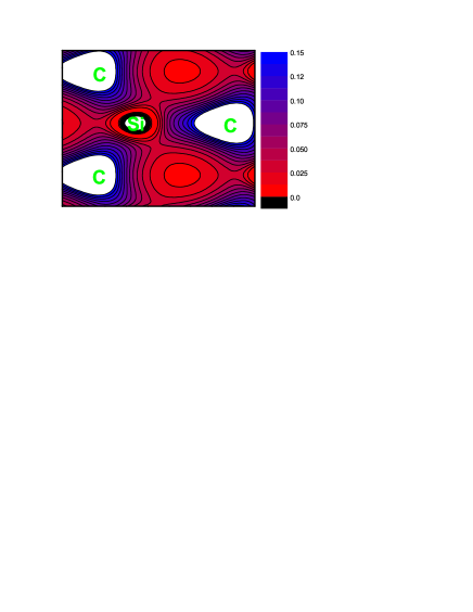
The charge density can be used to describe the distribution of electrons in real space, which is plotted Figure 6 for monolayer SiC. It is clearly seen that the charge density increases from Si atom to C atom, which means that charge transfer is produced between Si and C atoms when the Si-C bond is formed. The charge transfer from Si to C atom induces the strongly polarized covalent bond. For graphene, there is no charge transfer due to the same atom types to form bond. The strongly polarized covalent bond can give rise to larger phonon anharmonicity, and induces stronger intrinsic phonon-phonon scattering, which leads to lower of monolayer SiC with respect to graphene.
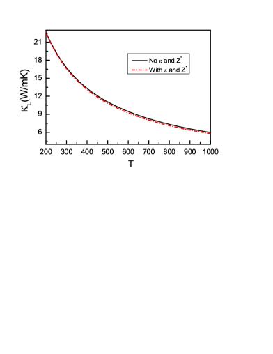
The dielectric constants and Born effective charges effects on lattice thermal conductivity are considered, as given in Table 1. The strongly polarized covalent bond can also be characterized by large and . The LO-TO splitting at the Brillouin zone center is produced by long-range electrostatic Coulomb interactions, which can be clearly seen in Figure 7. It is noted that the only has a slight change with or without and . It is because LO and TO branches have little contribution to total .
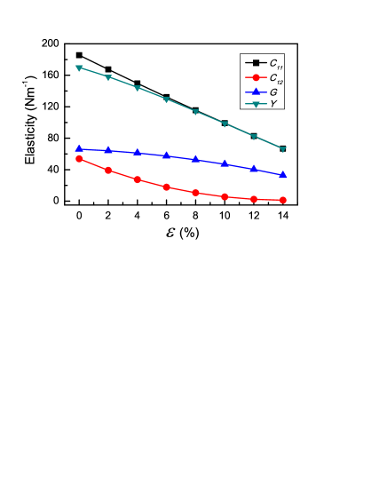
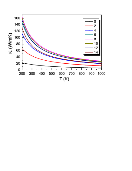
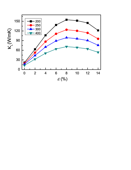
Strain can effectively tune in many 2D materialsq18 ; q18-1 ; q19 ; q19-1 ; q20 . The biaxial strain can be described by defining , in which is the unstrain lattice constant. Firstly, the strain dependence of elastic constants , Young’s moduli and shear modulus in SiC monolayer are plotted in Figure 8. They all monotonically decrease from 0% to 14% strain. In considered strain range, all the obtained elastic constants are positive, confirming the mechanical stability in strained SiC monolayer. The of the unstrained SiC monolayer is lower than those of h-BN and grapheneela , but higher than one of ela-1 . In the strain range of 0% - 14%, the of SiC monolayer as a function of temperature are plotted in Figure 9, together with vs strain at the temperature of 200, 250, 300 and 400 K. The shows a nonmonotonic trend with increased strain, and first increases from 16.75 (unstrained) to 99.15 (at 8% strain) then decreases to 75.61 (at 14% strain). Similar up-and-down behavior is also found in penta-q20 , -AsPq18-1 and bilayer graphenebg . The room-temperature at 8% strain is about 5.9 times that of the unstrained case.
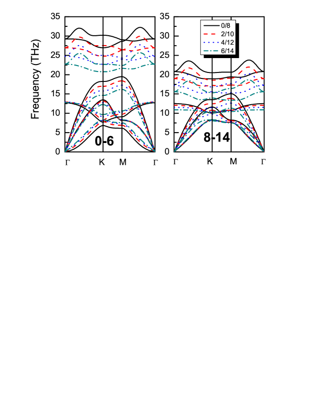
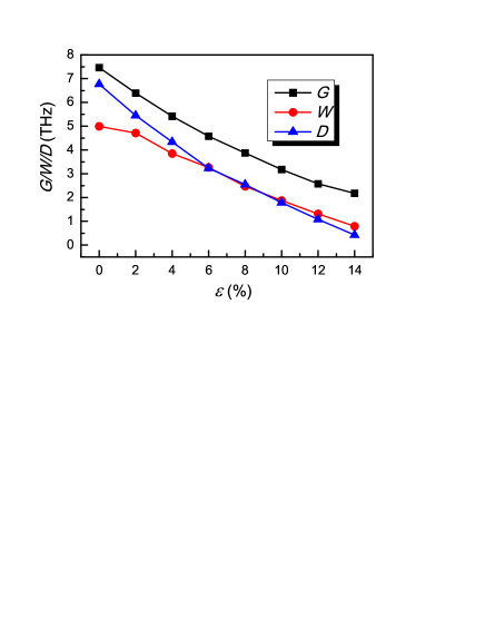
To identify the underlying mechanism of strain-dependent up-and-down behavior of in SiC monolayer, the phonon dispersions of SiC monolayer with 0%-14% strain are plotted Figure 10. It is clearly seen that there are no imaginary frequencies in considered strain range, indicating that strained SiC monolayer is dynamically stable. With increasing strain, the dispersions of both TA and LA modes are softened, producing the reduced phonon group velocities. The dispersion of ZA mode near point is stiffened, indicating the improved phonon group velocities. It is noted that the change of ZA mode at small strain is more obvious than one at large strain. These can also be observed in penta-grapheneq20 , AsPq18-1 and q19-1 . With strain increasing, the quadratic nature of ZA mode near the point disappears, which can also be found in AsP and q18-1 ; q19-1 . Due to less strongly interacting between atoms with increased strain, the dispersions of optical branches overall move toward low frequency. The phonon gap , the width of ZO mode , and the difference of maximum frequency between LA and ZO modes as a function of strain are plotted in Figure 11. It is clearly seen that they all decrease with increased strain, which can produce important effects on phonon transports of SiC monolayer. The large phonon gap hinders acoustic+acousticoptical (aao) scattering due to the energy conservation, which can enhance . The reduced with increased strain can give negative contribution to . The reduced and have positive contribution to due to reduced scattering channels for acoustic phonon.
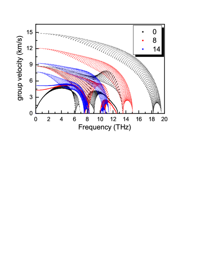
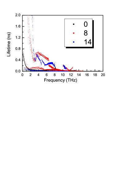
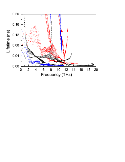
Due to dominant contribution to from modes below the phonon gap, we only show these phonon mode group velocities and phonon lifetimes with 0%, 8% and 14% strains in Figure 12 and Figure 13. Due to stiffened ZA dispersion, group velocities of ZA mode increase in low frequency region with increased strain. Near the point, the group velocity of ZA mode increases from 0.94 (0%) to 4.30 (6%) to 5.15 (10%). In high frequency region, most of group velocities of ZA mode increase from 0% to 8% strain, and have little change from 8% to 14% strain. Due to softened phonon dispersions, the reduced phonon group velocities of LA and TA branches are found with strain increasing. The phonon group velocities of ZO branch decrease with increased strain due to reduced . The reduction of most phonon group velocities have negative contribution to with increased strain. It is clearly seen that most of phonon lifetimes of SiC monolayer firstly increase, and then decrease. The strain dependence of phonon lifetimes is consistent with that of . The opposite effects on phonon lifetimes caused by the reduce of between and / lead to unusual strain dependence of phonon lifetimes. Through considering synthetically strain dependence of phonon group velocities and phonon lifetimes, at low strains (8%), the phonon lifetimes enhancement is responsible for increased , while at high strains (8%) the reduction of group velocities and phonon lifetimes results in decreased .
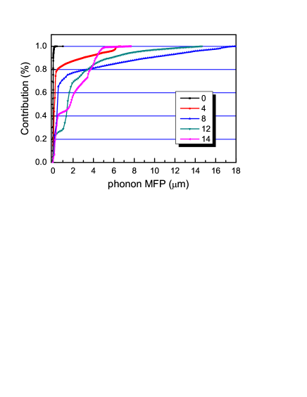
The ratio between cumulative and total lattice thermal conductivity of SiC monolayer with 0%, 4%, 8%, 12% and 14% strains as a function of phonon MFP are shown in Figure 14. With increased MFP, the ratio is close to one for all strains. The critical MFP firstly increases with increased strain, and then decreases, which is identical with . The critical MFP changes from 0.27 (unstrained) to 17.87 (at 8% strain), then drop to 7.45 (at 14% strain). The critical MFP at 8% strain is 66 times larger than unstrain that, demonstrating that strain can produce very strong size effects for of SiC monolayer. Similar results can also be found in antimonene, AsP monolayer, silicene, germanene and staneneq18 ; q18-1 ; q18-2 .
IV Conclusion
In summary, the first-principles calculations are performed to predict the of SiC monolayer under strain. The calculated room-temperature of monolayer SiC is substantially lower than that of graphene. The underlying mechanism for the low of monolayer SiC can be understood by the mode level phonon group velocities and lifetimes. We further perform analysis from the view of charge density distribution. Significantly different from that in graphene, there is very large charge transfer between Si and C atoms, forming the strongly polarized covalent Si-C bond. The strongly polarized Si-C bond gives rise to the low of monolayer SiC by inducing large phonon anharmonicity. Within 14% tensile strain, the of SiC monolayer first increases, and then decreases. The maximum is at 8% tensile strain, which is about 5.9 times that of the unstrained case. This trend of with increased strain is mainly due to the strain-dependent phonon lifetimes. Similar strain-dependent may also be found in GaN and ZnO monolayers with the same perfect planar hexagonal honeycomb structure. Our works will motivate farther experimental studies, and studies of phonon transports of other 2D materials with a perfect planar hexagonal honeycomb structure.
Acknowledgements.
This work is supported by the National Natural Science Foundation of China (Grant No.11404391). We are grateful to the Advanced Analysis and Computation Center of CUMT for the award of CPU hours to accomplish this work.References
- (1) K. S. Novoselov, A. K. Geim, S. V. Morozov, D. Jiang, Y. Zhang, S. V. Dubonos, I. V. Grigorieva and A. A. Firsov, Science 306, 666 (2004).
- (2) M. Chhowalla, H. S. Shin, G. Eda, L. J. Li, K. P. Loh and H. Zhang, Nature Chemistry 5, 263 (2013).
- (3) R. X. Fei, W. B. Li, J. Li and L. Yang, Appl. Phys. Lett. 107, 173104 (2015).
- (4) S. L. Zhang M. Q. Xie, F. Y. Li, Z. Yan, Y. F. Li, E. J. Kan, W. Liu, Z. F. Chen, H. B. Zeng, Angew. Chem. 128, 1698 (2016).
- (5) J. P. Ji, X. F. Song, J. Z. Liu et al., Nat. Commun. 7, 13352 (2016).
- (6) S. Balendhran, S. Walia, H. Nili, S. Sriram and M.Bhaskaran, small 11, 640 (2015).
- (7) Z. Y. Al Balushi, K. Wang, R. K. Ghosh, R. A. Vil, S. M. Eichfeld, J. D. Caldwell, X. Qin, Y.-C. Lin, P. A. DeSario, G. Stone, S. Subramanian, D. F. Paul, R. M. Wallace, S. Datta, J. M. Redwing and J. A. Robinson, Nat. Mater. 15, 1166 (2016).
- (8) M. Topsakal, S. Cahangirov, E. Bekaroglu and S. Ciraci, Phys. Rev. B 80, 235119 (2009).
- (9) Z. Yan, G. X. Liu, J. M. Khan and A. A. Balandin, Nat. Commun. 3, 827 (2012).
- (10) G. Qin, Z. Qin, W.-Z. Fang, L.-C. Zhang, S.-Y. Yue, Q.-B. Yan, M. Hu and G. Su, Nanoscale, 8, 11306 (2016).
- (11) B. Peng, H. Zhang, H. Z. Shao, Y. F. Xu, G. Ni, R. J. Zhang and H. Y. Zhu, Phys. Rev. B 94, 245420 (2016).
- (12) D. C. Zhang, A. X. Zhang, S. D. Guo and Y. F. Duan, RSC Adv. 7, 24537 (2017).
- (13) X. K. Gu and R. G. Yang, Appl. Phys. Lett. 105, 131903 (2014).
- (14) G. P. Li, K. L. Yao and G. Y. Gao, Nanotechnology 29, 015204 (2018).
- (15) G. P. Li, G. Q. Ding and G. Y. Gao, J. Phys.: Condens. Matter 29, 015001 (2017).
- (16) A. X. Zhang, J. T. Liu, S. D. Guo and H. C. Li, Phys. Chem. Chem. Phys. 19, 14520 (2017).
- (17) S. D. Guo, arXiv:1801.04455 (2018).
- (18) Y. D. Kuang, L. Lindsay, S. Q. Shic and G. P. Zheng, Nanoscale 8, 3760 (2016).
- (19) A. Shafique and Y. H. Shin, Phys. Chem. Chem. Phys. 19, 32072 (2017).
- (20) H. K. Liu, G. Z. Qin, Y. Lin and M. Hu, Nano Lett. 16, 3831 (2016).
- (21) H. M. Wang, G. Z. Qin, G. J. Li, Q. Wang and M. Hu, Phys. Chem. Chem. Phys. 19, 12882 (2017).
- (22) Z. Z. Qin, G. Z. Qin, X. Zuo, Z. H. Xiong and M. Hu, Nanoscale 9, 4295 (2017).
- (23) T. Susi, V. Skakalova, A. Mittelberger, P. Kotrusz, M. Hulman, T. J. Pennycook, C. Mangler, J. Kotakoski, J. C. Meyer, arXiv:1701.07387 (2017).
- (24) X. F. Wu, V. Varshney et al., Chem. Phys. Lett. 669, 233 (2017).
- (25) G. Kresse, J. Non-Cryst. Solids 193, 222 (1995).
- (26) G. Kresse and J. Furthmller, Comput. Mater. Sci. 6, 15 (1996).
- (27) J. P. Perdew, K. Burke and M. Ernzerhof, Phys. Rev. Lett. 77, 3865 (1996).
- (28) G. Kresse and D. Joubert, Phys. Rev. B 59, 1758 (1999).
- (29) A. Togo, L. Chaput and I. Tanaka, Phys. Rev. B 91, 094306 (2015).
- (30) A. Togo, F. Oba, and I. Tanaka, Phys. Rev. B 78, 134106 (2008).
- (31) S.I. Tamura, Phys. Rev. B, 27, 858 (1983).
- (32) Q. Peng, W. Ji, and S. De, Comput. Mater. Sci. 56, 11 (2012).
- (33) R. C. Andrew, R. E. Mapasha, A. M. Ukpong and N. Chetty, Phys. Rev. B 85, 125428 (2012).
- (34) S. D. Guo, arXiv:1801.01273 (2018).
- (35) Y. Kuang, L. Lindsay and B. Huang, Nano Lett. 15, 6121 (2015).
- (36) Y. D. Kuang, L. Lindsay, S. Q. Shic and G. P. Zheng, Nanoscale 8, 3760 (2016).