Characterization and Reduction of Capacitive Loss Induced by Sub-Micron Josephson Junction Fabrication in Superconducting Qubits
Abstract
Josephson junctions form the essential non-linearity for almost all superconducting qubits. The junction is formed when two superconducting electrodes come within 1 nm of each other. Although the capacitance of these electrodes is a small fraction of the total qubit capacitance, the nearby electric fields are more concentrated in dielectric surfaces and can contribute substantially to the total dissipation. We have developed a technique to experimentally investigate the effect of these electrodes on the quality of superconducting devices. We use /4 coplanar waveguide resonators to emulate lumped qubit capacitors. We add a variable number of these electrodes to the capacitive end of these resonators and measure how the additional loss scales with number of electrodes. We then reduce this loss with fabrication techniques that limit the amount of lossy dielectrics. We then apply these techniques to the fabrication of Xmon qubits on a silicon substrate to improve their energy relaxation times by a factor of 5.
Josephson junction (JJ) based superconducting qubits are a promising platform for quantum information processing.Kelly et al. (2015); Chow et al. (2014); Poletto et al. (2012); Fowler et al. (2012) Based on current performances a powerful and error protected processor will require millions of physical qubits.Fowler et al. (2012) This number depends strongly on the error rates of individual physical qubits. The ratio of gate operation time to qubit energy relaxation time () sets a limit on the operation’s fidelity. A dominant source of decoherence in superconducting devices is stray coupling to two level states (TLSs) in amorphous dielectrics.Martinis et al. (2005); Quintana et al. (2017); Megrant et al. (2012); Dial et al. (2016) Strong coupling to TLS defects near their resonant frequency also create ‘holes’ in tunable qubit spectra which restrict the frequencies available for control operations.Barends et al. (2013) Nanofabrication techniques such as photolithography, thin film deposition, and etching tend to leave 1-10 nanometer thick interfacial dielectric films with loss tangents on the order of , which are difficult to remove.Quintana et al. (2014) Large strides have been made to reduce the energy loss to these surface dielectrics leading to greatly enhanced ’s in planar and three dimensional superconducting resonators.Megrant et al. (2012); Reagor et al. (2013) While qubit ’s have also improved, they still lag behind those of resonators and appear to be limited by other loss channels.
A key difference between resonator and qubit circuits is the inclusion of JJs. Transmon qubits in particular have two main circuit elements: a linear capacitor and a non-linear inductive element typically constructed from one or more Al/AlOx/Al JJs. To create capacitors of the highest quality, planar capacitor fabrication can be separated from JJ fabrication and defined identically to planar resonators with critical dimensions of tens of microns.Barends et al. (2013); Kelly et al. (2015); Barends et al. (2014); Córcoles et al. (2015) Sub-micron JJs are then shadow evaporated and electrically shorted to the capacitor in a lift-off process. This processing is known to leave behind lossy dielectrics at the surrounding interfaces.Quintana et al. (2014) Furthermore, electrodes that connect to JJs come within close proximity of each other, concentrating electric fields in nearby interfaces and increasing loss.Wang et al. (2015) Thus, a large amount of loss can come from a relatively small amount of lossy material.
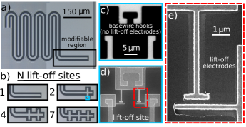
To quantify the additional loss associated with JJ electrodes we mimic the fabrication of JJs connected to high quality coplanar waveguide (CPW) resonators. We add small capacitive ‘lift-off sites’ to the open end of CPW resonators where there is an electric field anti-node. These lift-off sites emulate the electrodes leading up to but not including the pair of JJs in the superconducting quantum interference device (SQUID) at the base of Xmon transmon qubits (Fig. 1(c/d)). We measure how loss scales with multiple lift-off sites, effectively amplifying the loss over the background loss of the resonator. We quantify the loss associated with JJ fabrication and use this knowledge to guide improvements in the fabrication leading directly into improvements in Xmon ’s. The most dramatic improvements occur in Xmons fabricated on silicon substrates, where we see an increase in by a factor of 5.
We fabricate these resonators with aluminum base wiring on high resistivity (10 kcm) intrinsic (100) plane silicon substrates. Prior to loading for deposition, we sonicate bare wafers in acetone then isopropanol and rinse with deionized (DI) water. We then dip the wafers in a heated piranha solution, followed by a DI water, then buffered HF to remove the native oxide. Immediately after blow drying with nitrogen, we load the wafers into a high vacuum electron beam deposition tool and deposit 100 nm of aluminum. We pattern the coplanar wave guide (CPW) resonators, microwave feedline, and launch pads using optical lithography. We develop the resist in AZ 300 MIF (2% TMAH in water) developer. We take advantage of the fact that the developer attacks aluminum to wet etch the pattern in the same step as development.
Next we use electron beam lithography (EBL) to pattern electrodes which mimic JJs’. First, we optically pattern lift-off gold alignment marks, then we pattern and develop the JJ electrode sites using EBL.Barends et al. (2013) We then load the wafer back into the same high vacuum deposition tool used for base aluminum. We use an in-situ 400 V, 0.8 mA/cm2 argon ion mill to etch away the native AlOx to make DC contact between the etched base wire metal and the lift-off metal. Barends et al. (2013); Quintana et al. (2014); Chen et al. (2014a) We immediately deposit aluminum at normal incidence leaving a 300 nm gap between ground and signal electrodes which mimic the JJ wiring excluding the JJ itself. It is important to note that we do not make DC electrical contact between the resonator’s center trace and the ground plane. This gap as well as ion mill redeposited residue is displayed using a scanning electron microscope (SEM) image in Fig. 1(e). A more complete description of fabrication procedures is contained within the supplement.sup
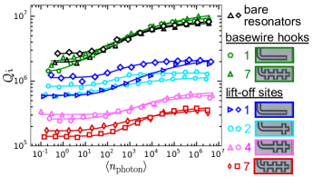
We show an example of a resonator structure in Fig. 1(a). This resonator is one of ten CPW resonators per chip, each capacitively coupled in parallel to a common feed-line. All resonators are designed with center trace width m, gap to the ground plane () on either side , and resonant frequencies () between 5.5 and 6.0 GHz. We fabricate CPW resonators with between zero and seven lift-off sites at the voltage anti-node to test the scaling of the additional loss with number of lift-off sites (Fig. 1(b)). The additional lift-off site structures (Fig. 1(b-d)) modify the circuit parameters slightly by adding a parallel capacitance to the open end, but this effect is small (1 % of the total resonator capacitance added per lift-off site). sup We cool these resonators in a heavily filteredBarends et al. (2011) adiabatic demagnetization refrigerator with a base temperature of 50 mK and extract their internal quality factor, by measuring and fitting the resonators’ scattering parameters versus frequency.Megrant et al. (2012); Chiaro et al. (2016) In Fig. 2 we plot this measured as a function of average photon occupation in the resonator. The low power plateau (around a single average photon occupation) approximates the loss experienced by qubits which also operate at a single photon.
The low power ’s of the bare resonators (with no lift-off sites) are within the device-to-device variation of bare resonators fabricated separately (between 2 and 3 million). These witnesses indicate that the fabrication process itself has little affect on the quality of bare resonators that are buried by resist during the lift-off processes. Additional base wire ‘hooks’ are used to connect lift-off to base wire aluminum (Fig. 1(c)). Resonators modified to include these hooks (without performing lift-off) have near the device-to-device variation of the bare resonators as well, indicating little to no added loss from modifying the base wire in this way. However, when lift-off metal is added, the asymptotic value of at low photon occupation scales inversely with the number of lift-off sites, and the additional low power loss () per site is 7.9.sup This increase of loss with number of JJ electrodes indicates qubits designed with SQUIDs will be twice as sensitive as those designed with single JJs.
The additional loss per lift-off site limits (the total internal quality of the resonator), given by:
| (1) |
where is the background loss from other sources, (the participation) is the ratio of electric field energy stored in the th volume to the total capacitive energy and is the dielectric loss of the th volume. The volume of dielectric between the electrodes is small due to their close proximity, and this small volume may not always contain TLSs sufficiently near resonance to contribute loss.Martinis et al. (2005) In Fig. 2 we see evidence of this effect when only a single pair of JJ electrodes is added the extracted single photon varies by over a factor of two between resonators at slightly different frequencies. Adding more sites scales the field energy stored near these electrodes and thus loss due to these interfaces approach a ‘loss tangent regime’ where Eq. 1 is valid. With enough lift-off sites the total loss of the resonator is dominated by this added loss and will be less dependent on individual TLS fluctuators.
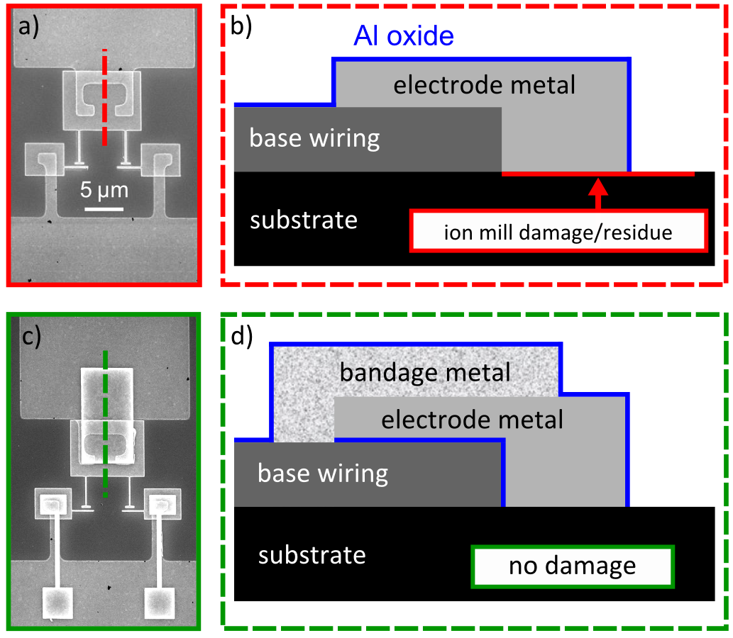
Previous work has shown that aggressive milling of the substrate leads to amorphization and thus added loss at the substrate-metal (SM) and nearby substrate-vacuum (SV) interfaces on sapphire substrates.Quintana et al. (2014) Using similar experiments on a silicon substrate we found this aggressive ion milled lift-off leaves a roughly 3.9 nm thick interfacial layer underneath the metal. Using cross-sectional finite-element simulations assuming a relative permittivity for this layer we extract an intrinsic TLS loss tangent .sup
To avoid creating this lossy interfacial layer while still making DC contact to the base wiring we break the electrode deposition into two distinct steps: ‘wiring’ and ‘bandage’. In the wiring step, we use EBL to define the same JJ electrodes as before, but without any in-situ argon mill. We use a downstream oxygen asher to descum the developed resist prior to loading the wafer for deposition. It has been shown that with no in-situ cleaning a de-scum prior to loading can be used to remove any left over contamination from the development process Koppinen et al. (2007); Pop et al. (2012) and reduce loss at interfaces.Quintana et al. (2014) After aluminum deposition we lift-off the resist and unwanted metal in solvents. Second, we use the bandage step to make galvanic contact between the newly deposited lift-off metal and the base wiring. We perform a second round of EBL lift-off, but only expose both metal surfaces (base wiring and JJ electrode). We aggressively ion mill (as detailed above) prior to the bandage deposition. The substrate is protected by resist and the new bandage metal electrically shorts the JJ electrodes to the base wiring (Fig. 3(c/d)). The lithography for the bandage metal can also be done optically and this process has been implemented during the JJ fabrication for Xmon, gmon Chen et al. (2014b), and fluxmonQuintana et al. (2017) qubits.
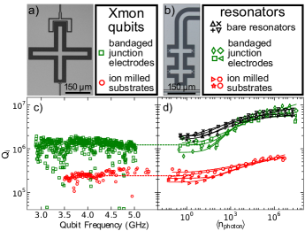
To test the improvement in quality from the bandage process we fabricate resonators with 4 lift-off sites and measure the resulting Qi’s (Fig. 4(c/d)). The low power Qi’s are raised back up to around (a factor of around 5 improvement from the lift-off damaged sites). A typical Xmon capacitor geometry is shown in Fig. 4(a). In Fig. 4(b) we plot corresponding to measurements sup of qubits that underwent both styles of fabrication. The average for these qubits is representative of qubits after these processes. The total capacitances of Xmons and the resonators indicate that resonators with 4 lift-off sites have similar lift-off site participation as qubits sup , and the magnitude of improvement is consistent with the average of low power internal quality factor measurements of these resonators (Fig. 4(c)).
Although the bandage process improves greatly, there still appears to be residual loss caused by the JJ electrodes limiting below that of the bare resonators, indicating further improvements are possible. There are also sections of the bandaged qubit spectrum where the drops far below it’s average value. These holes occur as the qubits transition frequency () is tuned through the resonance of a particularly strongly coupled TLS.Barends et al. (2013) The tunability of the qubit allows for probing loss as a function of frequency while each resonator only probes at a single frequency.
In summary, we modified resonators to use them as a tool to directly measure the added capacitve loss from JJ electrodes necessary for most superconducting qubits. We used this tool to measure different JJ electrode fabrication techniques and found that aggressive ion milling of silicon substrates adds substantial loss. We developed an improved process where we protect the substrate from aggressive ion milling without altering the high coherence capacitor fabrication. We fabricated qubits using this process and measured the average increase by a factor of 5.
This work was supported by Google. C. Q. and Z. C. acknowledge support from the National Science Foundation Graduate Research Fellowship under Grant No. DGE-1144085. Devices were made at the UC Santa Barbara Nanofabrication Facility, a part of the NSF funded National Nanotechnology Infrastructure Network.
References
- Kelly et al. (2015) J. Kelly, R. Barends, A. Fowler, A. Megrant, E. Jeffrey, T. White, D. Sank, J. Mutus, B. Campbell, Y. Chen, et al., Nature 519, 66 (2015).
- Chow et al. (2014) J. M. Chow, J. M. Gambetta, E. Magesan, D. W. Abraham, A. W. Cross, B. Johnson, N. A. Masluk, C. A. Ryan, J. A. Smolin, S. J. Srinivasan, et al., Nature communications 5 (2014).
- Poletto et al. (2012) S. Poletto, J. M. Gambetta, S. T. Merkel, J. A. Smolin, J. M. Chow, A. Córcoles, G. A. Keefe, M. B. Rothwell, J. Rozen, D. Abraham, et al., Physical review letters 109, 240505 (2012).
- Fowler et al. (2012) A. G. Fowler, M. Mariantoni, J. M. Martinis, and A. N. Cleland, Physical Review A 86, 032324 (2012).
- Martinis et al. (2005) J. M. Martinis, K. Cooper, R. McDermott, M. Steffen, M. Ansmann, K. Osborn, K. Cicak, S. Oh, D. Pappas, R. Simmonds, et al., Physical Review Letters 95, 210503 (2005).
- Quintana et al. (2017) C. Quintana, Y. Chen, D. Sank, A. Petukhov, T. White, D. Kafri, B. Chiaro, A. Megrant, R. Barends, B. Campbell, et al., Physical Review Letters 118, 057702 (2017).
- Megrant et al. (2012) A. Megrant, C. Neill, R. Barends, B. Chiaro, Y. Chen, L. Feigl, J. Kelly, E. Lucero, M. Mariantoni, P. O’Malley, et al., Applied Physics Letters 100, 113510 (2012).
- Dial et al. (2016) O. Dial, D. T. McClure, S. Poletto, G. Keefe, M. B. Rothwell, J. M. Gambetta, D. W. Abraham, J. M. Chow, and M. Steffen, Superconductor Science and Technology 29, 044001 (2016).
- Barends et al. (2013) R. Barends, J. Kelly, A. Megrant, D. Sank, E. Jeffrey, Y. Chen, Y. Yin, B. Chiaro, J. Mutus, C. Neill, et al., Physical review letters 111, 080502 (2013).
- Quintana et al. (2014) C. Quintana, A. Megrant, Z. Chen, A. Dunsworth, B. Chiaro, R. Barends, B. Campbell, Y. Chen, I.-C. Hoi, E. Jeffrey, et al., Applied Physics Letters 105, 062601 (2014).
- Reagor et al. (2013) M. Reagor, H. Paik, G. Catelani, L. Sun, C. Axline, E. Holland, I. M. Pop, N. A. Masluk, T. Brecht, L. Frunzio, et al., Applied Physics Letters 102, 192604 (2013).
- Barends et al. (2014) R. Barends, J. Kelly, A. Megrant, A. Veitia, D. Sank, E. Jeffrey, T. White, J. Mutus, A. Fowler, B. Campbell, et al., arXiv preprint arXiv:1402.4848 (2014).
- Córcoles et al. (2015) A. D. Córcoles, E. Magesan, S. J. Srinivasan, A. W. Cross, M. Steffen, J. M. Gambetta, and J. M. Chow, Nature communications 6 (2015).
- Wang et al. (2015) C. Wang, C. Axline, Y. Y. Gao, T. Brecht, Y. Chu, L. Frunzio, M. Devoret, and R. Schoelkopf, Applied Physics Letters 107, 162601 (2015).
- Chen et al. (2014a) Z. Chen, A. Megrant, J. Kelly, R. Barends, J. Bochmann, Y. Chen, B. Chiaro, A. Dunsworth, E. Jeffrey, J. Mutus, et al., Applied Physics Letters 104, 052602 (2014a).
- (16) See supplementary material.
- Barends et al. (2011) R. Barends, J. Wenner, M. Lenander, Y. Chen, R. C. Bialczak, J. Kelly, E. Lucero, P. O’Malley, M. Mariantoni, D. Sank, et al., Applied Physics Letters 99, 113507 (2011).
- Chiaro et al. (2016) B. Chiaro, A. Megrant, A. Dunsworth, Z. Chen, R. Barends, B. Campbell, Y. Chen, A. Fowler, I. Hoi, E. Jeffrey, et al., Superconductor Science and Technology 29, 104006 (2016).
- Koppinen et al. (2007) P. Koppinen, L. Väistö, and I. Maasilta, Applied physics letters 90, 053503 (2007).
- Pop et al. (2012) I.-M. Pop, T. Fournier, T. Crozes, F. Lecocq, I. Matei, B. Pannetier, O. Buisson, and W. Guichard, Journal of Vacuum Science & Technology B, Nanotechnology and Microelectronics: Materials, Processing, Measurement, and Phenomena 30, 010607 (2012).
- Chen et al. (2014b) Y. Chen, C. Neill, P. Roushan, N. Leung, M. Fang, R. Barends, J. Kelly, B. Campbell, Z. Chen, B. Chiaro, et al., Physical review letters 113, 220502 (2014b).