-
May 2016
Shortcut to adiabaticity in full-wave optics for ultra-compact waveguide junctions
Abstract
We extend the concept of shortcut to adiabaticity to full-wave optics and provide application to the design of an ultra-compact waveguide junction. In particular, we introduce a procedure allowing one to synthesize a purely dielectric optical potential that precisely compensates for the non-adiabatic losses of the transverse-electric fundamental mode in any (sufficiently regular) two-dimensional waveguide junction. Our results are corroborated by finite-element method numerical simulations in a Pöschl-Teller waveguide mode expander.
Keywords: Inhomogeneous optical media; Gradient-index media; Integrated optics devices.
The adiabatic theorem guarantees that if a system changes sufficiently slowly its eigenstates smoothly evolve without coupling to each others [1, 2, 3]. This concept has been widely exploited in many different areas of physics, from quantum mechanics to optics [4]. As example, a gently-tapered waveguide allows one to efficiently convert a narrow waveguide mode into a broader one (or viceversa), which is a key functionality in optical interconnects [5, 6, 7]. Several photonic structures based on the adiabatic evolution of light waves have been reported [8, 9, 10, 11, 12, 13, 14, 15, 16], including asymmetric y-branch couplers [9], 4-port filters and multiplexers [10, 11], broadband splitters and filters [12, 13, 14, 15], and densely-packed sub wavelength waveguides [16], just to mention a few. Adiabatic protocols are very robust against variation of parameters [17] but suffer from a fundamental limitation in terms of speed, which in optics translates into a minimum length of the device, thus posing a major issue for its exploitation in integrated optics.
A technique leading to a substantial speeding of the adiabatic evolution is referred to as Shortcut To Adiabaticity (STA). The concept of STA was originally introduced in quantum mechanics, and refers to a family of methods including, among others, Counterdiabatic or Transitionless Tracking [18, 19, 20, 21, 22], Invariant-Based Inverse Engineering [23, 24], and Fast-Forward Approach [25, 26, 27] (see also Ref. 28 and references therein). Very recently, the STA has been reported in other physical contexts, including non-hermitian quantum physics [29, 30] and, most interestingly, optics [31, 32, 33, 34, 35]. The exploitation of STA in optics can led to much more compact waveguide devices as compared to the corresponding adiabatic structures, which is very beneficial to device integration. However, the optical STA has been limited to finite-dimensional systems where the dynamics of light transport is reduced to coupled-mode-equations (CMEs) formalism, allowing a precise mimicking of STA protocols already developed in quantum mechanics.
In this letter we extend the optical STA to full-wave problems for the Helmholtz equation, i.e. to an infinite dimensional system. The analysis is pursued in a two dimensional space and for transverse electric (TE) fields. Our optical STA is exemplified by designing an efficient ultra-compact waveguide expander, where the radiation losses induced by shortening of an adiabatic configuration are compensated by superposing a suitable optical potential.
We consider an optical medium with translational invariance along one direction, , and electromagnetic waves propagating in the plane (a so called in-plane wave propagation problem). For isotropic media the TE-TM decomposition holds, allowing one to reduce the general case to two decoupled scalar diffraction problems, one for the TE polarization (non zero electric field out of the plane) and one for the TM polarization (non zero magnetic field out of the plane). We limit our analysis to the TE case but, in principle, a similar approach can be pursued for the TM case as well (even though with a more complicated numerical approach that should deserve a dedicated study). In the time-harmonic regime for TE waves, the non zero electric field component obeys the Helmholtz equation:
| (1) |
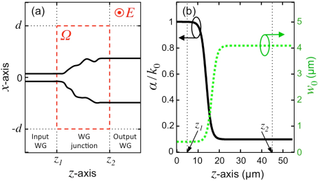
where is the optical pulsation, is the speed of light in vacuum, is the relative permittivity of the medium and the subscript denotes partial derivative with respect to the space coordinates. Let’s now consider the special case of a dielectric function having a very slow and smooth variation along (the optical axis) from to , and being -invariant out of the interval. The section between and is thus interpreted as a junction between an input () waveguide and an output () waveguide [Fig. 1(a)]. If the junction fulfills adiabatic conditions (see below), the electric field evolves adiabatically along the structure:
| (2) |
where and are, respectively, the field profile and effective index of the local normal mode at around the considered coordinate. More precisely, if we denote the dielectric function of the adiabatic structure as , and obey the following eigenvalue equation parametrized by :
| (3) |
If the optical potential is purely real, the adiabatic waveguide junction is lossless, but ought to be very long in order to fulfill adiabatic conditions. The latter can be derived by inserting Eq. (2) into Eq. (1), leading, in the most general case, to an optical potential made of the sum of two terms, the adiabatic potential plus an extra potential that accounts for deviations from adiabaticity (if any):
| (4) |
Note that , i.e. is negligible with respect to , provided that the evolution of and along is slow enough, and this requires the waveguide junction (i.e. the distance between and ) to be several orders of magnitude longer than the optical wavelength . In case of non adiabatic evolution of , the adiabatic field of Eq. (2) is no more an approximated solution to Eq. (1), and the waveguide junction becomes lossy: the input mode couples to other guided modes (if any), including back propagating modes in the input section, and to radiating modes.
The seek for a shortcut to adiabaticity corresponds to the finding of a suitable optical potential that superimposed to exactly compensates for the losses induced by non adiabaticity. Obviously, one can simply take . However, since is complex valued and with both the real and the imaginary parts that depends on and , this approach to STA is challenging to implement in a physical device, since it would require a complex control of spatially dispersed gain and loss in the medium. A viable approach to STA in the present context would provide a real valued . To this aim, we pursue an idea inspired to the streamlined version of the Fast-Forward STA introduced for the Schrödinger equation by Torrontegui et al. [27]. Let’s assume, instead of Eq. (2) a more general ansatz for the electric field propagating in the waveguide structure:
| (5) |
with a real-valued phase field to be determined under suitable boundary conditions. Note that above ansatz guarantees an evolution of the light intensity which is precisely that of a fast-forward adiabatic passage across the waveguide junction, since as for the field of Eq. (2). By inserting Eq. (5) into Eq. (1) and setting a complex valued equation is retrieved for the complex valued STA potential . We can thus exploit the degree of freedom provided by the field to nullify the imaginary part of , which results into the following partial differential equation in the unknown:
| (6) |
where . Provided that above equation can be solved with suitable boundary conditions, the resulting field is used to compute the non-zero part of , which is now purely real and reads as follows:
| (7) |
Interestingly, Eq. (6) is a very-well known partial differential equation, that is the time-invariant convection-diffusion equation, for which several boundary value problems (BVP) have been extensively studied (see e.g. Ref. 36). Note that, according to Eqs. (6)-(7), the field is not uniquely defined, because the gauge transformation leads to the same STA potential. To guarantee the phase matching between the local normal mode and the propagating fields at the edges of the waveguide junction, one can impose . Also, one should require the optical STA potential to be localized within a certain distance from the optical axis. To do so we impose . Above conditions identify a Neumann BVP for the field on the domain in the plane [Fig. 1(a)]. To provide gauge fixing and thus guarantee uniqueness of the solution, one of the Newmann boundary conditions was replaced with a Dirichlet one by setting , which translates into a mixed BVP. It is worth pointing out that since in any waveguide structure the profile of the fundamental (local) normal mode can be assumed to be positively defined, Eq. (6) turns out to be elliptic in the wall domain. Therefore, provided that the field is smooth with its derivatives, standard methods of variational analysis based on the Lax-Milgram theorem guarantee that the mixed BVP above defined is well-posed [36], and the search for a numerical solution can be pursued by, e.g., finite-element method (FEM) numerical analysis.
To exemplify our approach to the optical STA problem we apply above method to a Pöschl-Teller (PT) waveguide and realize an ultra-compact mode-expander. A PT waveguide shows the following dielectric profile [37]:
| (8) |
where is the refractive index of the waveguide cladding and is a -dependent parameter exploited to control the evolution of the waveguide structure. As is well known [37], such a waveguide admits of a single mode whose adiabatic evolution according to Eq. (2) is ruled by:
| (9) | |||||
| (10) |
In the above equations, , (i.e. the mode effective index of the input waveguide) and is an arbitrary constant (in V/m).
To design a mode-expander for the PT waveguide one can evolve the parameter from a high value to a low value along the -axis. As example, we take:
| (11) |
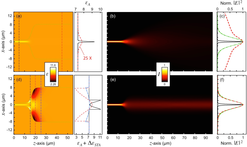
where , and and determine the spatial extent of the waveguide junction. An implementation of above formula with (being m the optical wavelength in vacuum), , m and is shown in Fig. 1(b) (solid line). This provides, by means of Eq. (8) with , the optical potential of Fig. 2(a). To a high degree of accuracy such an optical potential turns out to be -invariant for m and for m, the input and output waveguides respectively. The waveguide junction [between the vertical dashed lines in Fig. 2(a)] is thus only m long (i.e. ). Also, note that the junction connects a very narrow waveguide with high permittivity core [solid curve in the inset of Fig. 2(a)] to a much broader waveguide with low permittivity core [dashed curve in the inset of Fig. 2(a)]. This structure largely violates the adiabatic conditions and the power launched on the mode of the input waveguide spreads on radiative modes after crossing the junction [Fig. 2(b)], with the result that the transmitted field at m [dashed curve in Fig. 2(c)] has poor superposition with the mode field of the output waveguide [dashdot curve in Fig. 2(c)].
A shortcut to adiabaticity for such a non adiabatic optical potential is realized by the dielectric function shown in Fig. 2(d), which is computed according to Eqs. (6)-(7) and (9)-(11) by FEM numerical analysis with Comsol Multiphysics 3.5. To make the implementation of our method feasible in a high refractive index material like, e.g., silicon, the retrieved from the computed by numerical integration of Eq. (6) was truncated to zero out of the region where the adiabatic local normal mode of Eq. (10) carries most of its energy. This is the region of the plane between the dotted curves in Fig. 2(a) and (d), where , being (i.e. the half width of the local normal mode at ), which is shown in Fig. 1(b) (dotted line). Note that the total optical potential exhibits both positive and negative variations with respect to the cladding permittivity [inset in Fig. 2(d)]. To ascertain that the STA potential thus obtained is capable of compensating the radiation losses caused by deviations to adiabaticity of the potential, we performed FEM propagation analysis for the structure of Fig. 2(d) when launching the input waveguide mode. The resulting light intensity pattern along the structure is shown in Fig. 2(e). It well reproduces the adiabatic pattern detailed by Eqs. (9)-(10), and the field transmitted by the junction [dashed line in Fig. 2(f)] has very high (almost unitary) overlap with the mode field of the output waveguide [dashdot line in Fig. 2(f)]. Note that the junction is designed to operate at m telecom wavelength and allows one to efficiently expand a narrow mode of m diameter to a 10 times broader one within a distance of [Fig. 1(b)].
Finally, it is worth noting that the gradient index structure of the waveguide junction of Fig. 2(d) can be fabricated by etching subwavelength holes in a silicon slab waveguide (see, e.g., Ref. 38 and references therein).
To conclude, we introduced in full-wave optics a method for shortcut to adiabaticity for an infinite dimensional system. Our method is developed for TE waves in a generic optical structure with a continuous translational invariance along one direction. The idea is applied to design an ultra-compact junction connecting a high permittivity core input waveguide to a weakly-guiding output waveguide of the kind of Pöschl-Teller. The junction is designed by superposing to the squeezed adiabatic configuration a gradient index optical potential (the STA potential) that precisely compensates for the losses induced by the geometrical squeezing of the adiabatic structure. Further developments in the field should consider the case of TM polarization and eventually an extension of our method to three-dimensional optical structures.
References
References
- [1] Born M and Fock V A 1928 Beweis des Adiabatensatzes Zeitschrift für Physik A 51 165
- [2] Kato T 1950 On the Adiabatic Theorem of Quantum Mechanics J. Phys. Soc. Jpn. 5 435
- [3] Griffiths D J 1995 Introduction to Quantum Mechanics (Upper Saddle River: Prentice Hall) p 323
- [4] Menchon-Enrich R, Benseny A, Ahufinger V, Greentree A D, Busch T and Mompart J 2016 Spatial adiabatic passage: a review of recent progress arXiv:1602.06658v1.
- [5] Jedrzejewski K P, Martinez F, Minelly J D, Hussey C D and Payne F P 1986 Tapered-beam expander for single-mode optical-fibre gap devices Electron. Lett. 22 105
- [6] Love J D and Henry W M 1986 Quantifying loss minimisation in single-mode fibre tapers Electron. Lett. 17 912
- [7] Birks T A and Li Y W 1992 The Shape of Fiber Tapers J. Lightwave Tech. 10 432
- [8] Hope A P, Nguyen T G, Greentree A D and Mitchell A 2013 Long-range coupling of silicon photonic waveguides using lateral leakage and adiabatic passage Opt. Express 21 22705
- [9] Love J D, Vance R W C and Joblin A 1996 Asymmetric, adiabatic multipronged planar splitters, Opt. Quantum Electron. 28 353
- [10] Adar R, Henry C H, Kazarinov R F, Kistler R C and Weber G R 1992 Adiabatic 3-dB couplers, filters, and multiplexers made with silica waveguides on silicon J. Lightwave Technol. 10 46
- [11] Yerolatsitis S, Gris-Sánchez I and Birks T A 2014 Adiabatically-tapered fiber mode multiplexers Opt. Express 22 608
- [12] Dreisow F, Ornigotti M, Szameit A, Heinrich M, Keil R, Nolte S, Tünnermann A and Longhi S 2009 Polychromatic beam splitting by fractional stimulated Raman adiabatic passage Appl. Phys. Lett. 95 261102
- [13] Longhi S 2006 Adiabatic passage of light in coupled optical waveguides Phys. Rev. E 73 026607
- [14] Ciret C, Coda V, Rangelov A A, Neshev D N and Montemezzani G 2012 Planar achromatic multiple beam splitter by adiabatic light transfer Opt. Lett. 37 3789
- [15] Menchon-Enrich R, Llobera A, Vila-Planas J, Cadarso V J, Mompart J and Ahufinger V 2013 Light spectral filtering based on spatial adiabatic passage Light: Sci. Appl. 2 e90
- [16] Mrejen M, Suchowski H, Hatakeyama T, Wu C, Feng L, O’Brien K, Wang Y and Zhang X 2015 Adiabatic elimination-based coupling control in densely packed subwavelength waveguides Nat. Commun. 6 7565
- [17] Vitanov N V, Rangelov A A, Shore B W and Bergmann K 2016 Stimulated Raman adiabatic passage in physics, chemistry and beyond arXiv:1605.00224
- [18] Demirplak M and Rice S A 2003 Adiabatic Population Transfer with Control Fields J. Chem. Phys. A 107 9937
- [19] Demirplak M and Rice S A 2005 Assisted Adiabatic Passage Revisited J. Phys. Chem. B 109 6838
- [20] Demirplak M and Rice S A 2008 On the consistency, extremal, and global properties of counterdiabatic fields J. Chem. Phys. 129 154111
- [21] Berry M V 2009 Transitionless quantum driving J. Phys. A: Math. Theor. 42 365303
- [22] Bason M G, Viteau M, Malossi N, Huillery P, Arimondo E, Ciampini D, Fazio R, Giovannetti V, Mannella R and Morsch O 2012 High-fidelity quantum driving Nature Phys. 8 147
- [23] Chen X, Ruschhaupt A, Schmidt S, del Campo A, Guéry-Odelin D and Muga J G 2010 Fast Optimal Frictionless Atom Cooling in Harmonic Traps: Shortcut to Adiabaticity Phys. Rev. Lett. 104 063002
- [24] Torrontegui E, Ibáñez S, Chen X, Ruschhaupt A, Guéry-Odelin D and Muga J G 2011 Fast atomic transport without vibrational heating Phys. Rev. A 83 013415
- [25] Masuda S and Nakamura K 2010 Fast-forward of adiabatic dynamics in quantum mechanics Proc. R. Soc. A 466 1135
- [26] Masuda S and Nakamura K 2011 Acceleration of adiabatic quantum dynamics in electromagnetic fields Phys. Rev. A 84 043434
- [27] Torrontegui E, Martínez-Garaot S, Ruschhaupt A and Muga J G 2012 Shortcuts to adiabaticity: fast-forward approach, Phys. Rev. A 86 013601
- [28] Muga J G et al. 2013 Shortcuts to Adiabaticity Advances in Atomic, Molecular and Optical Physics vol 62 ed E Arimondo, P R Berman and C C Lin (Chennai: Academic Press)
- [29] Torosov B T, Della Valle G and Longhi S 2013 Non-Hermitian shortcut to adiabaticity Phys. Rev. A 87 052502
- [30] Torosov B T, Della Valle G and Longhi 2014 Non-Hermitian shortcut to stimulated Raman adiabatic passage Phys. Rev. A 89 063412
- [31] Lin T-Y, Hsiao F-C, Jhang Y-W, Hu C and Tseng S-Y 2012 Mode conversion using optical analogy of shortcut to adiabatic passage in engineered multimode waveguides Opt. Express 20 24085
- [32] Stefanatos D 2014 Design of a photonic lattice using shortcuts to adiabaticity Phys. Rev. A 90 023811
- [33] Tseng S-Y 2014 Robust coupled-waveguide devices using shortcuts to adiabaticity Opt. Lett. 39 6600
- [34] Yeih C-S, Cao H-X and Tseng S-Y 2014 Shortcut to Mode Conversion via Level Crossing in Engineered Multimode Waveguides IEEE Photon. Technol. Lett. 26 123
- [35] Paul K and Sarma A K 2015 Shortcut to adiabatic passage in a waveguide coupler with a complex-hyperbolic-secant scheme Phys. Rev. A 91 053406
- [36] Salsa S 2009 Partial Differential Equations in Action: From Modelling to Theory (Milano: Springer) p 454
- [37] Lekner J 2007 Reflectionless eigenstates of the sech2 potential Am. J. Phys. 75 1151
- [38] Valentine J, Li J, Zentgraf T, Bartal G and Zhang X 2009 An optical cloak made of dielectrics Nature Mater. 8 568