Structural and electronic properties of germanene on MoS2
Abstract
To date germanene has only been synthesized on metallic substrates. A metallic substrate is usually detrimental for the two-dimensional Dirac nature of germanene because the important electronic states near the Fermi level of germanene can hybridize with the electronic states of the metallic substrate. Here we report the successful synthesis of germanene on molybdenum disulfide (MoS2), a band gap material. Pre-existing defects in the MoS2 surface act as preferential nucleation sites for the germanene islands. The lattice constant of the germanene layer (3.8 0.2 Å) is about 20% larger than the lattice constant of the MoS2 substrate (3.16 Å). Scanning tunneling spectroscopy measurements and density functional theory calculations reveal that there are, besides the linearly dispersing bands at the points, two parabolic bands that cross the Fermi level at the point.
pacs:
73.22.-f, 81.05.Zx, 68.37.EfThe discovery that graphene, a single layer of hybridized carbon atoms arranged in a honeycomb registry, is stable has resulted in numerous intriguing and exciting scientific breakthroughs een ; twee . The electrons in graphene behave as relativistic massless fermions that are described by the Dirac equation, i.e. the relativistic variant of the Schrödinger equation. One might anticipate that elements with a similar electronic configuration, such as silicon (Si), germanium (Ge) and tin (Sn), also have a “graphene-like” allotrope. Unfortunately, silicene (the silicon analogue of graphene), germanene (the germanium analogue of graphene) and stanene (the tin analogue of graphene) have not been found in nature and therefore these two-dimensional (2D) materials have to be synthesized. Theoretical calculations have revealed that the honeycomb lattices of the “graphene-like” allotropes of silicon and germanium are not fully planar, but slightly buckled drie ; vier . The honeycomb lattices of these 2D materials consist of two triangular sub-lattices that are slightly displaced with respect to each other in a direction normal to the honeycomb lattice. Despite this buckling the 2D Dirac nature of the electrons is predicted to be preserved drie ; vier . Another salient difference with graphene is that silicene and germanene have a substantially larger spin-orbit gap than graphene (0.05 meV). Silicene’s spin-orbit gap is predicted to be 1.55 meV, whereas the predicted spin-orbit gap of germanene is even 23.9 meV. This is very interesting because graphene and also silicene and germanene are in principle 2D topological insulators and thus ideal candidates to exhibit the quantum spin Hall effect. The interior of a 2D topological insulator exhibits a spin-orbit gap, whereas topologically protected helical edge modes exist at the edges of the material vijf ; zes . The two topologically protected spin-polarized edge modes have opposite propagation directions and therefore the charge conductance vanishes, whereas the spin conductance has a non-zero value.
In the past few years various groups have successfully synthesized silicene zeven ; acht ; negen and germanene tien ; elf ; twaalf ; dertien on a variety of substrates. To date germanene has only been grown on metallic substrates, such as Pt(111) tien , Au(111) elf , Ge2Pt twaalf ; veertien and Al(111) dertien , which might hinder a proper decoupling of the key electronic states of germanene near the Fermi level from the underlying substrate. Only Bampoulis et al. twaalf managed to resolve the primitive cell of the buckled honeycomb structure of germanene.
Here we report the growth of germanene on a band gap material, namely MoS2. We found that the germanene layer, which is only weakly coupled to the MoS2 substrate, exhibits a clear V-shaped density of states. These experimental observations are in very good agreement with density functional theory calculations. The synthesis of germanene on MoS2 is a first step towards future germanene-based device applications.
The scanning tunneling microscopy (STM) and spectroscopy (STS) experiments have been performed at room temperature with an ultra-high vacuum STM (Omicron STM-1). The base pressure of the ultra-high vacuum system is 3 10-11 mbar. We have used electrochemically etched tungsten STM tips. The MoS2 samples were freshly cleaved from synthesized 2H-MoS2 (acquired from 2D Semiconductors) and mounted on a Mo sample holder and subsequently introduced into the ultra-high vacuum system. Ge was deposited onto the MoS2 substrate, which was held at room temperature, by resistively heating a clean Ge(001) wafer at 1150 K. The Ge wafer was located at a distance of 10 mm from the MoS2 substrate. Prior to the deposition the Ge(001) wafer was cleaned by a pre-anneal at 700 K for about 24 h followed by several cycles of argon ion bombardment at 800 eV at room temperature and annealing at 1100 K vijftien . After the deposition of germanium, the MoS2 sample was immediately inserted into the STM. The deposition rate was estimated by analyzing several STM images after the deposition of sub-monolayer amounts of germanium on the MoS2 substrate.
The density functional theory (DFT) calculations were performed using the projected augmented wave (PAW) formalism zestien as implemented in the Vienna Ab Initio Simulation Package (VASP) zeventien ; achttien . Exchange-correlation effects were taken into account within the dispersion-corrected nonlocal optB88-vdW functional negentien . An energy cutoff of 600 eV for the plane-waves and a convergence threshold of 10-5 eV were employed. To avoid interactions between the supercells, a 25 Å thick vacuum slab was added in the direction normal to the surface. The Brillouin zone was sampled by a (4 4) k-point mesh. Structural relaxation was performed, while keeping the lowermost layer of sulfur atoms fixed, until the forces acting on the other atoms were less than 10-2 eV/Å.
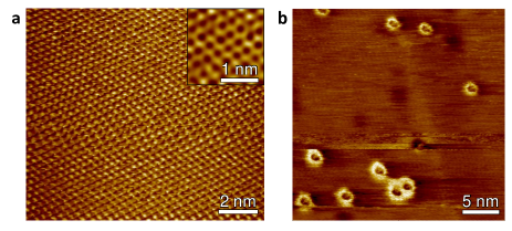
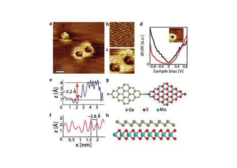
Figure 1(a) shows an empty state STM image of the molybdenum disulfide (MoS2) substrate. MoS2 is a transition metal dichalcogenide. The elementary building block of a MoS2 crystal is a tri-layer structure consisting of one close-packed Mo atomic layer encapsulated between two atomic layers of close-packed S atoms (see Figure 2(g)-(h)). The atoms within this layer are strongly bonded by covalent interactions, whereas the interactions between the MoS2 layers are governed by weak Van der Waals forces. MoS2 can easily be exfoliated and has a band gap that varies from 1.2 eV to 1.8 eV depending on its thickness. In most cases only the S-atoms of MoS2 substrate are resolved in STM images, resulting in a triangular structure with a lattice constant of 3.16 Å. In the inset of Figure 1(a) a high resolution STM image of the primitive honeycomb cell of MoS2 is shown. The natural exfoliated MoS2 surface usually contains some defects that are caused by a local variation in the stoichiometry, missing atoms or impurities. These defects can lead to -type as well as -type doping and are studied in depth twintig ; twintig1 ; twintig2 . The defects affect the electronic structure of the MoS2 in the vicinity of the defects and therefore they appear usually substantially larger in STM images than they really are (see Figure 1(b)). In Figure 1(b) a MoS2 substrate is shown after the deposition of 10 % of a monolayer of germanium at room temperature (here one monolayer corresponds to a (5 5) cell of germanene on a (6 6) cell of the MoS2 substrate). Several germanium islands have been nucleated at pre-existing defects of the MoS2 substrate. From image to image the shape and size of these germanium islands changes, which implies (1) attachment and detachment of germanium atoms at the edges of the germanium islands and (2) rapid diffusion of germanium atoms across the surface. Interestingly, there is a hexagonal shaped vacancy island in the center of all the nucleated germanium islands.
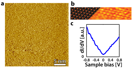
Figure 2(a) shows a small scale STM image of the MoS2/germanium substrate. The frizzy appearance of the germanium islands is clearly visible. We cannot exclude that part of this dynamics is induced by the scanning process. In the upper left part of the image a germanium island changes abruptly in size. In Figures 2(b)-(c) zoom-ins of a germanium-free part of the MoS2 substrate and a germanium island are shown, respectively. The lattice constant of the germanium islands is 20 % larger than the lattice constant of the MoS2 substrate, i.e. 3.8 0.2 Å for germanium versus 3.16 Å for MoS2. The germanium islands exhibit a threefold symmetry as the underlying MoS2 substrate does. In addition, the high symmetry directions of the MoS2 substrate and the germanium islands are aligned (see Figure 2(a)).
Differential conductivity (dI/dV) spectra recorded on a germanium island and the bare MoS2 substrate are depicted in Figure 2(d). As expected the MoS2 region has a band gap, whereas the differential conductivity of the germanium island reveals a well-defined V-shape around zero bias ( 0.5 V). For small sample biases the differential conductivity is proportional to the density of states and therefore also the density of states of the germanium islands exhibits a V-shape, which is one of the hallmarks of a 2D Dirac system. Based on these observations we arrive at the conclusion that the germanium islands are actually germanene islands. This assignment does, however, not imply that these germanene islands also exhibit all the interesting and intriguing “graphene” properties.
In figure 2(e)-(f) line scans taken across the germanene island (see Figure 2(a)) are depicted. The apparent height of the germanene island is 3.2 Å. Since the electronic structure of germanene and MoS2 are substantially different it is not appropriate to compare this experimentally determined step height with theoretical predictions.
In Figure 3(a)-(b) an STM image is shown after the deposition of 1 monolayer of germanium. The germanene islands are now much larger and virtually the whole MoS2 surface is covered with germanene. The hexagonal shaped vacancy islands have all disappeared. The periodicity of the structure in Figure 3(a)-(b) is again 3.8 0.2 Å. It is pointed out that the resolution in Figure 3(a) is somewhat lower than in the previous images. In Figure 3(b) only one of the two triangular sub-lattices is resolved. We did not find any evidence for the presence of a moiré pattern. Due to the 20 % difference in lattice constants between germanene and MoS2 one expects only very small moiré periodicities ( 2 nm) twintig3 .
As shown in Figure 3(c) the differential conductivity has a well-defined V-shape and thus confirms our earlier assignment that we are dealing with germanene. The differential conductivity does, however, not completely vanish at the Dirac point indicating that the system is metallic and hence not an ideal 2D Dirac system. Free-standing low-buckled germanene is known to be a 2D Dirac system that shares many properties with its famous counterpart graphene twintig4 . Here we are dealing with a germanene layer on a substrate and even though the interaction between germanene and MoS2 is rather weak, the structural and electronic properties of germanene are affected by the substrate.
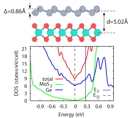
To support our experimental observations of germanene, we have performed first-principles calculations using DFT. Unlike earlier DFT studies, where germanene has been considered on MoS2 in its free-standing configuration with a lattice constant of 3.97 Åtwintig5 ; twintig6 , we consider here germanene laterally contracted by 5 % in accordance with the experimental observations. Particularly, we use a (5 5) unit cell of germanene placed on top of a (6 6) unit cell of a MoS2 monolayer with a lattice constant = 3.18 Å, which yields a contracted germanene lattice constant Å. Subsequently we optimize the atomic structure by taking Van der Waals interactions into account and find an average equilibrium buckling parameter of germanene Å and a corresponding interlayer distance Å, defined as the distance between the in-plane averaged centers of mass of germanene and MoS2.
The density of states (DOS) is depicted in Figure 4 and shows a pronounced V-shape in the energy range of 1 eV near the Fermi energy stemming from electronic states of germanium. Moreover, the shape of both germanene and MoS2 DOS are found to be in very good agreement with the experimental dI/dV spectra shown in Figure 2(d). Moreover, the non-zero DOS at the Dirac point observed in experimental spectra is also reproduced. The only difference concerns the position of the Fermi energy, which is shifted in the calculated DOS toward higher energies by 0.3 eV. This shift indicates an -type doping of the system. The absence of such a shift in the experimental spectra can be associated with the presence of acceptor impurities (e.g., O) or unsaturated defects in the sample.
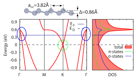
To gain more insight into the origin of the finite DOS at the Dirac point as well as the observed doping, we calculate the band structure and perform orbital analysis of contracted free-standing germanene with the above mentioned structural parameters and . The results are shown in Figure 5. In addition to the -bands leading to the formation of a Dirac cone in the vicinity of the K-point, there are two -bands close to the -point. The emergence of those bands is related to the relatively large buckling of germanene, which makes the occupation of -states energetically less favorable twintig4 and leads to a - charge transfer. As a consequence of this process, the Fermi energy is shifted relative to the Dirac point, whereas unoccupied -bands produce a finite DOS in the relevant energy region. The -states contribution to the DOS is weakly dependent on energy as the corresponding dispersion is nearly quadratic (). Therefore, we conclude that the observed V-shape of the total DOS originates predominantly from the -states of germanene.
After having performed the STM and STS measurements we took the MoS2/germanene sample out of the ultra-high vacuum system for an ex-situ analysis. X-ray photoelectron spectroscopy measurements revealed that the germanene has been oxidized. As a final remark we want to point out that hexagonal boron nitride is another very appealing substrate for the synthesis of germanene twintig7 . Hexagonal boron nitride has a band gap of 5.9 eV and a nearly perfect lattice match with germanene.
In summary, we have synthesized large continuous layers of germanene on a band gap material. The germanene islands preferentially nucleate at pre-existing defects of the MoS2 surface. Germanene’s lattice constant is about 20 % larger than that of MoS2 and the angle between the two lattices is 0 degrees. The density of states of the germanene layer exhibits a well-defined V-shape around the Fermi level, which hints to a 2D Dirac system. Unfortunately, the buckled germanene layer also has two parabolic bands that cross the Fermi level at the point. These states might suppress the anomalous quantum Hall effect as well as the 2D Dirac transport properties.
Acknowledgements.
LZ and QY thank the China Scholarship Council for financial support. PB thanks the Nederlandse Organisatie voor Wetenschappelijk Onderzoek (NWO, STW 11431) for financial support. HJWZ and MIK thank the stichting voor Fundamenteel Onderzoek der Materie (FOM, FV157) for financial support. ANR and MIK acknowledge financial support by the European Union Seventh Framework Programme under Grant Agreement No. 604391 Graphene Flagship.References
- (1) K.S. Novoselov, A.K. Geim, S.V. Morozov, D. Jiang, Y. Zhang, S.V. Dubonos, I.V. Grigoreva and A.A. Firsov, Science 306, 666 (2004)
- (2) A.K. Geim and K.S. Novoselov, Nat. Mater. 6, 183 (2007)
- (3) G.G. Guzmán-Verri and L.C. Lew Yan Voon, Phys. Rev. B 76, 075131 (2007)
- (4) S. Cahangirov, M. Topsakal, E. Aktürk, H. Sahin and S. Ciraci, Phys. Rev. Lett. 102, 236804 (2009)
- (5) C.L. Kane and E.J. Mele, Phys. Rev. Lett. 95, 146802 (2005)
- (6) C.L. Kane and E.J. Mele, Phys. Rev. Lett. 95, 226801 (2005)
- (7) P. Vogt, P. De Padova, C. Quaresima, J. Avila, E. Frantzeskakis, M. C. Asensio, A. Resta, B. Ealet, and G. Le Lay, Phys. Rev. Lett. 108, 155501 (2012)
- (8) A. Fleurence, R. Friedlein, T. Ozaki, H. Kawai, Y. Wang, Y. Yamada-Takamura, Phys. Rev. Lett. 108, 245501 (2012)
- (9) D. Chiappe, E. Scalise, E. Cinquanta, C. Grazianetti, B. van den Broek, M. Fanciulli, M. Houssa and A. Molle, Adv. Mater 26, 2096 (2014)
- (10) L. Li, S.-Z. Lu, J. Pan, Z. Qin. Y.-Q. Wang, Y. Wang, G. Cao, S. Du ad H.-J. Gao, Adv. Mater 26, 4820 (2014)
- (11) M.E. Dávila, L. Xian, S. Cahangirov, A. Rubio and G. Le Lay, New J. Phys. 16, 095002 (2014)
- (12) P. Bampoulis, L. Zhang, A. Safaei, R. van Gastel B. Poelsema and H.J.W. Zandvliet, J. Phys. Cond. Mat. 26, 442001 (2014)
- (13) M. Derivaz, D. Dentel, R. Stephan, M.-C. Hanf, A. Mehdaoui, P. Sonnet, and C. Pirri, Nano Lett 15, 2510 (2015)
- (14) L. Zhang, P. Bampoulis, A. van Houselt and H.J.W. Zandvliet, Appl. Phys. Lett. 107, 111605 (2015)
- (15) H.J.W. Zandvliet, Phys. Rep. 388, 1 (2003)
- (16) P.E. Blöchl, Phys. Rev. B 50, 17953 (1994)
- (17) G. Kresse and J. Furthüller, Phys. Rev. B 54, 11169 (1996)
- (18) G. Kresse and D. Joubert, Phys. Rev. B 59, 1758 (1999)
- (19) J. Klimeš, D.R. Bowler, and A. Michaelides, Phys. Rev. B 83, 195131 (2011)
- (20) M.-H. Whangbo, J. Ren, S.N. Magonov, H. Bengel, B.A. Parkinson and A. Suna, Surf. Science 326 311 (1995)
- (21) R. Addou, L. Colombo and R.M. Wallace, ACS Appl. Interf. 7, 11921 (2015) and references therein
- (22) J. Lin, S.T. Pantelides and W. Zhou, ACS Nano 9, 5189 (2015)
- (23) M. Yankowitz, J. Xue, D. Cormode, J.D. Sanchez-Yamagishi, K. Watanabe, T. Taniguchi, P. Jarillo-Herrero, P. Jacquod and B.J. LeRoy, Nature Phys. 8, 381 (2012)
- (24) A. Acun, L. Zhang, P. Bampoulis, M. Farmanbar, M. Lingenfelder, A. van Houselt, A.N. Rudenko, G. Brocks, B. Poelsema, M.I. Katsnelson and H.J.W. Zandvliet, J. Phys. Cond. Mat. 27, 443002 (2015) and references therein
- (25) X. Li, S. Wu, S. Zhou and Z. Zhu, Nanoscale Res. Lett. 9, 110 (2014)
- (26) X.D. Li, S.Q. Wu, Z.Z. Zhu, J. Mater. Chem. C 3, 9403 (2015)
- (27) M. Corso, W. Auwärter, M. Muntwiler, A. Tamai, T. Greber and J. Osterwalder, Science 303, 217 (2004)