Temporal correlation detection using computational phase-change memory
Abstract
For decades, conventional computers based on the von Neumann architecture have performed computation by repeatedly transferring data between their processing and their memory units, which are physically separated. As computation becomes increasingly data-centric and as the scalability limits in terms of performance and power are being reached, alternative computing paradigms are searched for in which computation and storage are collocated. A fascinating new approach is that of computational memory where the physics of nanoscale memory devices are used to perform certain computational tasks within the memory unit in a non-von Neumann manner. Here we present a large-scale experimental demonstration using one million phase-change memory devices organized to perform a high-level computational primitive by exploiting the crystallization dynamics. Also presented is an application of such a computational memory to process real-world data-sets. The results show that this co-existence of computation and storage at the nanometer scale could be the enabler for new, ultra-dense, low power, and massively parallel computing systems.
In today’s computing systems based on the conventional von Neumann architecture (Fig. 1(a)), there are distinct memory and processing units. The processing unit comprises the arithmetic and logic unit (ALU), a control unit and a limited amount of cache memory. The memory unit typically comprises dynamic random-access memory (DRAM), where information is stored in the charge state of a capacitor. Performing an operation (such as an arithmetic or logic operation), , over a set of data stored in the DRAM, , to obtain the result, , requires a sequence of steps in which the data must be obtained from the memory, transferred to the processing unit, processed, and stored back to the memory. This results in a significant amount of data being moved back and forth between the physically separated memory and processing units. This costs time and energy, and constitutes an inherent bottleneck in performance.
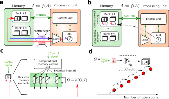 |
To overcome this, a tantalizing prospect is that of transitioning to a hybrid architecture where certain operations, such as , can be performed at the same physical location as where the data is stored (Fig. 1(b)). Such a memory unit that facilitates such collocated computation is referred to as computational memory. There are recent reports of the use of DRAM to perform bulk bit-wise operations Y2016seshadriArXiV and fast row copying Y2013seshadriISM within the DRAM chip. However, a new class of emerging nanocale devices, namely, resistive memory or memristive devices with their multi-level and non-volatile storage capability as well as sufficient richness of dynamics are particularly well suited for computational memory. In these devices, information is stored in their resistance/conductance states and these devices can remember the history of the current that has flowed through them Y2008strukovNature ; Y2011chuaAPA ; Y2015wongNatureNano .
The essential idea behind computational memory is not to treat memory as a passive storage entity, but to exploit the dynamics of the memory devices to realize computation exactly at the place where the data is stored. The data is stored in the conductance state of the device, denoted by , as in a conventional memory unit, and the computational task (e.g. ) is performed by applying appropriate electrical signals that “imprint” the result of the computation in the very same memory device (Fig. 1(c)). For example, to implement additive arithmetics, accumulative dynamics can be used whereby the conductance evolves monotonically as a function of the number of electrical pulses applied to the devices (Fig. 1(d)). Besides its collocated nature, this type of computation is massively parallel, and achieves high areal/power efficiency as well as speed.
An early proposal for the use of memristive devices for in-place computing was the realization of certain logical operations using a circuit based on TiOx-based memory devices Y2010borghettiNature . The same memory devices are used simultaneously to store the inputs, perform the logic operation, and store the resulting output. More complex logic units based on this initial concept were proposed Y2014kvatinskyTCAS ; Y2016zhaICCAD ; Y2016vourkasIEEECSM . Implementations of logical operations using other physical phenomena were also proposed, such as ferroelectric domain switching induced by the tip of a scanning probe microscope Y2014ievlevNatPhys and the crystallizationY2013ielminiAM and melting Y2014lokePNAS of phase-change materials. In these memristive logic applications, one exploits only the binary resistance states of the devices. Matrix vector multiplication using Ohm’s law and Kirchhoff’s law is another computational primitive that can be realized very efficiently using resistive memory devices. Massively parallel, memory-centric hardware accelerators based on this concept are now becoming an important subject of research Y2015burrITED ; Y2016shafieeISCA ; Y2016chiISCA ; Y2016bojnordiHPCA ; Y2017burrAPX . However, to date, a few experimental reports go beyond a proof-of-concept demonstration.
In this paper, we present an algorithm whereby the crystallization dynamics of a type of resistive memory device, namely, phase-change memory (PCM) devices, are exploited to implement a high-level computational primitive. Subsequently, we present a large-scale experimental demonstration of the computational memory concept using an array of one million PCM devices. We also present an application of such a computational memory to process real-world data-sets such as weather data.
I Results
Dynamics of phase-change memory devices
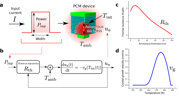 |
A PCM device consists of a nanometric volume of phase-change material sandwiched between two electrodes. A schematic illustration of a PCM device with mushroom-type device geometry is shown in Fig. 2(a)) Y2016burrJETCAS . In an as-fabricated device, the material is in the crystalline phase. When a current pulse of sufficiently high amplitude is applied to the PCM device (typically referred to as the RESET pulse), a significant portion of the phase-change material melts due to Joule heating. When the pulse is stopped abruptly, the molten material quenches into the amorphous phase because of glass transition. In the resulting RESET state, the device will be in the low conductance state as the amorphous region blocks the bottom electrode. The size of the amorphous region is captured by the notion of an effective thickness, Y2011sebastianJAP . PCM devices exhibit a rich dynamic behavior with an interplay of electrical, thermal and structural dynamics that forms the basis for their application as computational memory. The electrical transport exhibits a strong field and temperature dependence Y2015legalloNJP . Joule heating and the thermal transport pathways ensure that there is a strong temperature gradient within the PCM device. Depending on the temperature in the cell, the phase-change material undergoes structural changes, such as phase transitions and structural relaxation Y2014sebastianNatComm ; Y2015ratyNatComm .
In our demonstration, we focus on a specific aspect of the PCM dynamics: the crystallization dynamics capturing the progressive reduction in the size of the amorphous region due to the amorphous to crystalline phase transition (Fig. 2(b)). When a current pulse (typically referred to as the SET pulse) is applied to a PCM device in the RESET state such that the temperature reached in the cell via Joule heating is high enough, but below the melting temperature, a part of the amorphous region crystallizes. At the nanometer scale, the crystallization mechanism is dominated by crystal growth due to the large amorphous–crystalline interface area and the small volume of the amorphous region Y2014sebastianNatComm . The crystallization dynamics in such a PCM device can be approximately described by
| (1) |
where denotes the temperature-dependent growth velocity of the phase-change material; is the temperature at the amorphous–crystalline interface, and is the initial effective amorphous thickness Y2014sebastianNatComm . is the ambient temperature, and is the effective thermal resistance that captures the thermal resistance of all possible heat pathways. Experimental estimates of and are shown in Fig. 2(c) and Fig. 2(d), respectively Y2014sebastianNatComm . From the estimate of as a function of , one can infer that the hottest region of the device is slightly above the bottom electrode and that the temperature within the device monotonically decreases with increasing distance from the bottom electrode. The estimate of shows the strong temperature dependence of the crystal growth rate. Up to approx. 550 K, the crystal growth rate is negligible whereas it is maximum at approx. 750 K. As a consequence of Equation (1), progressively decreases upon the application of repetitive SET pulses and hence the low-field conductance progressively increases. In subsequent discussions, the RESET and SET pulses will be collectively referred to as write pulses. It is also worth noting that in a circuit-theoretic representation, the PCM device can be viewed as a generic memristor, with serving as an internal state variable Y2015corintoJETCAS ; Y2016ascoliIJCTA .
Detecting statistical correlations using computational memory
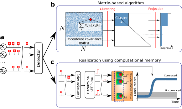 |
In this section, we show how the crystallization dynamics of PCM devices can be exploited to perform a high-level computational task, such as that of detecting statistical correlations between event-based data streams. Such problems arise in a multitude of application areas such as, the Internet of Things (IoT), life sciences, networking, social networks and large scientific experiments Y2014lazerScience . For example, one could generate an event-based data stream based on the presence or absence of a specific word in a collection of tweets. Sensory data processing is another promising application area, especially with sensors such as the dynamic vision sensor Y2010liuCON . One can also view correlation detection as a key constituent of unsupervised learning where one of the objectives is to find correlated clusters in data streams.
In a generic formulation of the problem, let us assume that there are discrete-time binary stochastic process arriving at a correlation detector (see Fig. 3(a)). Let be one of the processes. Then is a random variable with probabilities
| (2) | |||||
| (3) |
for . Let be another discrete-time binary stochastic processes with the same value of parameter . Then the correlation coefficient of the random variables and at time instant is defined as
| (4) |
Processes and are said to be correlated if or uncorrelated otherwise. The objective of the correlation detection problem is to detect, in an unsupervised manner, an unknown subset of these processes that are mutually correlated.
As schematically illustrated in Fig. 3(b), one way to solve this problem is by obtaining an estimate of the uncentered covariance matrix corresponding the processes denoted by
| (5) |
Next, by summing the elements of this matrix along a row or column, we can obtain certain numerical weights corresponding to the processes denoted by . It can be shown that if belongs to the correlated group with correlation coefficient , then
| (6) |
denotes the number of processes in the correlated group. In contrast, if belongs to the uncorrelated group, then
| (7) |
Hence by monitoring in the limit of large , we can determine which processes are correlated with . Moreover, it can be seen that with increasing and , it becomes easier to determine whether a process belongs to a correlated group.
We can show that this rather sophisticated problem of correlation detection can be efficiently solved using a computational memory module comprising PCM devices by exploiting the crystallization dynamics. By assigning each incoming process to a single PCM device, the statistical correlation can be calculated and stored in the very same device as the data passes through the memory. The way it is achieved is schematically depicted in Fig. 3(c): At each time instance, , a “collective momentum”, , that corresponds to the instantaneous sum of all processes is calculated. The calculation of incurs little computational effort as it just counts the number of non-zero events at each time instance. Next, an identical SET pulse is applied potentially in parallel to all the PCM devices for which the assigned binary process has a value of 1. The duration or amplitude of the SET pulse is chosen to be a linear function of . For example, let the duration of the pulse, . For the sake of simplicity, let us assume that the interface temperature, , is independent of the amorphous thickness, . As the pulse amplitude is kept constant, , where is a constant. Then from Equation 1, the absolute value of the change in the amorphous thickness of the phase-change device at the discrete-time instance is
| (8) |
The total change in the amorphous thickness after time steps can be shown to be
| (9) | |||||
Experimental platform
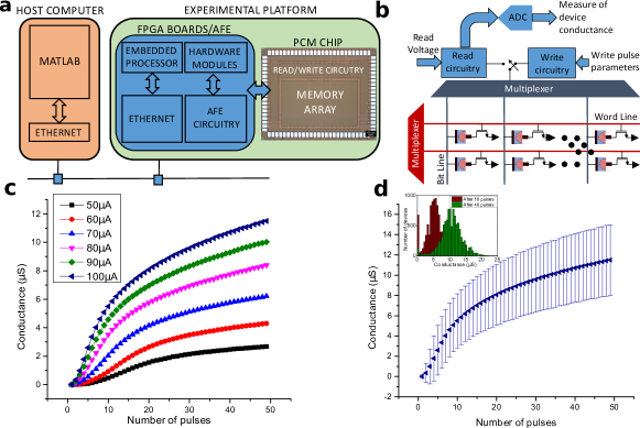 |
Next, we present experimental demonstrations of the concept. The experimental platform (schematically shown in Fig. 4(a)) is built around a prototype PCM chip that comprises 3 million PCM devices. More details on the chip are presented in the methods section. As shown in Fig. 4(b)), the PCM array is organized as a matrix of word lines (WL) and bit lines (BL). In addition to the PCM devices, the prototype chip integrates the circuitry for device addressing and for write and read operations. The PCM chip is interfaced to a hardware platform comprising two field programmable gate array (FPGA) boards and an analog-front-end (AFE) board. The AFE board provides the power supplies as well as the voltage and current reference sources for the PCM chip. The FPGA boards are used to implement the overall system control and data management as well as the interface with the data processing unit. The experimental platform is operated from a host computer, and a Matlab environment is used to coordinate the experiments.
An extensive array-level characterization of the PCM devices was conducted prior to the experimental demonstrations. In one experiment, 10,000 devices were arbitrarily chosen and were first RESET by applying a rectangular current pulse of 1 s duration and 440 A amplitude. After RESET, a sequence of SET pulses of 50 ns duration were applied to all the devices, and the resulting device conductance values were monitored after the application of each pulse. The map between the device conductance and the number of pulses is referred to as an accumulation curve. The accumulation curves corresponding to different SET currents are shown in Fig. 4(c). These results clearly show that the mean conductance increases monotonically with increasing SET current (in the range from 50 A and 100 A) and with increasing number of SET pulses. From Fig. 4(d), it can also be seen that there is significant variability associated with the evolution of the device conductance values. This variability arises from inter-device as well as intra-device variability. The intra-device variability is traced to the differences in the atomic configurations of the amorphous phase created via the melt-quench process after each RESET operation Y2016tumaNatureNano ; Y2016legalloESSDERC . Besides the variability arising from the crystallization process, additional fluctuations in conductance also arise from noise Y2010closeIEDM and drift variability Y2012pozidisIMW .
Experimental demonstration with a million correlated processes
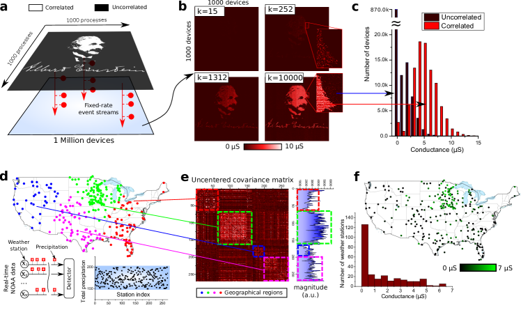 |
In a first demonstration of correlation detection, we created the input data artificially, and generated one million binary stochastic processes organized in a two-dimensional grid (Fig. 5(a)). We arbitrarily chose a subset of 95,525 processes, which we mutually correlated with a relatively weak instantaneous correlation coefficient of 0.1, whereas the other 904,475 were uncorrelated. The objective was to see if we can detect these correlated processes using the computational memory approach. Each stochastic process was assigned to a single PCM device. First, all devices were RESET by applying a current pulse of 1 s duration and 440 A amplitude. In this experiment, we chose to modulate the SET current while maintaining a constant pulse duration of 50 ns. At each time instance, the SET current is chosen to be equal to A, where is equal to the collective momentum. This rather simple calculation was performed in the host computer. Alternatively, it could be done in one of the FPGA boards. Next, the on-chip write circuitry was instructed to apply a SET pulse with the calculated SET current to all the PCM devices for which . To minimize the execution time, we chose not to program the devices if the SET current is less than 25 A. The SET pulses were applied sequentially. However, if the chip has multiple write circuitries that can operate in parallel, then it is also possible to apply the SET pulses in parallel. This process of applying SET pulses was repeated at every time instance. The maximum SET current applied to the devices during the experiment was 80 A.
As described earlier, owing to the temporal correlation between the processes, the devices assigned to those processes are expected to go to a high conductance state. We periodically read the conductance values of all PCM devices using the on-chip read circuitry and the on-chip ADC. The resulting map of the conductance values are shown in Fig. 5(b). Also shown is the corresponding distribution of the conductance values (Fig. 5(c)). This distribution shows that we can distinguish between the correlated and the uncorrelated processes. The inaccuracies are attributed to the variability and conductance fluctuations discussed earlier. However, it is remarkable that in spite of these issues, we are able to perform the correlation detection with significantly high accuracy. Note that there are several applications, such as sensory data processing, where these levels of accuracy could be sufficient. Moreover, there are also ways to improve the accuracy by using multiple devices to interface with a single random process. The conductance fluctuations can also be minimized using concepts such as projected phase change memory Y2015koelmansNatComm .
Another issue is that of the limited dynamic range of the conductance values. There is a limit to the and hence the maximum conductance values that the devices can achieve. The accumulation curves in Fig. 4(d) clearly show that the mean conductance values begin to saturate after the application of a certain number of pulses. This means that the correlations have to be detected within a reasonable amount of time dictated by this “dynamic range”. Hence, once the correlation has been detected, then the devices need to be RESET, and the operation has to be resumed to detect subsequent correlations. The application of shorter SET pulses is one way to increase the dynamic range. Unfortunately, in the PCM chip we experimented with, we were limited to a minimum pulse width of 50 ns. The use of multiple devices to interface with the random processes can also enlarge the dynamic range.
As per Equation (6), we would expect the level of separation between the distributions of correlated and uncorrelated groups to increase with increasing values of the correlation coefficient. This could be experimentally confirmed. The experimental results show that the correlated groups can be detected down to very low correlation coefficients such as even though it will be difficult to make a precise evaluation of the correlation coefficient. Moreover, this concept could potentially also be used to detect multiple correlated groups having different correlation coefficients.
Experiment with the weather data
A second demonstration is based on real-world data from 270 weather stations across the USA. Over a period of 6 months, the rainfall data from each station constituted a binary stochastic process that was applied to the computational memory at one-hour time steps. The process took the value 1 if rainfall occurred in the preceding one-hour time window, else it was 0 (Fig. 5(d)). An analysis of the uncentered covariance matrix shows that several correlated groups exist and that one of them is predominant. As expected, also a strong geographical correlation with the rainfall data exists (Fig. 5(e)). Correlations between the rainfall events are also reflected in the geographical proximity between the corresponding weather stations. To detect the predominant correlated group using computational memory, we used the same approach as above, but with 4 PCM devices interfacing with each weather station data. The four devices were used to improve the accuracy. At each instance in time, the SET current was calculated to be equal to A. Next, the PCM chip was instructed to program the devices sequentially with the calculated SET current. The on-chip write circuitry applies a write pulse with the calculated SET current to all PCM devices for which . We chose not to program the devices if the SET current is less than 25 A. The duration of the pulse was fixed to be 50 ns, and the maximum SET current applied to the devices was 80 A. The resulting device conductance map (averaged over the four devices per weather station) shows that the conductance values corresponding to the predominant correlated group of weather stations are comparably higher (Fig. 5(f)).
Based on a threshold conductance value chosen to be 2 S, we can classify the weather stations into correlated and uncorrelated weather stations. We can also make comparisons with established unsupervised classification techniques such as -means clustering. It was seen that, out of the 270 weather stations, there was a match for 245 weather stations. The computational memory approach classified 12 stations as uncorrelated which were marked correlated by the -means clustering approach. Similarly, the computational memory approach classified 13 stations as correlated which were marked uncorrelated by the -means clustering approach. Given the simplicity of the computational memory approach, it is remarkable that it can achieve this level of similarity with such a sophisticated and well-established classification algorithm.
II Discussion
The scientific relevance of the presented work is that we have convincingly demonstrated the ability of computational memory to perform certain high-level computational tasks in a non-von Neumann manner by exploiting the dynamics of resistive memory devices. We have also demonstrated the concept experimentally at the scale of a million PCM devices. Even though in the experimental demonstrations using the prototype chip, we programmed the devices sequentially, we could also program them in parallel given the availability of sufficient number of write modules. A hypothetical computational memory module performing correlation detection need not be substantially different from conventional memory modules. The main constituents of such a module will also be a memory controller and a memory chip. Tasks such as computing can easily be performed in the memory controller. The memory controller can then convey the write/read instructions to the memory chip. It can be shown that in such a computational memory module, we could accelerate the correlation detection task by a factor of 200 compared to state-of-the-art computing hardware. In order to quantify the time, we measured the performance of various different implementations that can be executed on an IBM Power System S822LC system. This system has 2 POWER8 CPUs (each comprising 10 cores) and 4 Nvidia Tesla P100 graphical processing units (attached using the NVLink interface).
An alternate approach to using PCM devices will be to design an application-specific chip where the accumulative behavior of PCM is emulated using complementary metal-oxide semiconductor (CMOS) technology using adders and registers. However, even at a relatively large 90 nm-technology node, the areal footprint of the computational phase-change memory is much smaller than that of CMOS-only approaches even though the dynamic power consumption is comparable. By scaling the devices to smaller dimensions and by using shorter write pulses, these gains are expected to increase several fold Y2011xiongScience ; Y2012lokeScience . The ultra-fast crystallization dynamics and non-volatility ensure a multi-time-scale operating window ranging from a few tens of nanoseconds to years. These attributes are particularly attractive for slow processes, where the leakage of CMOS would dominate dynamic power because of low utilization rate.
It can be shown that a single-layer spiking neural network can also be used to detect temporal correlations Y2003guetigJN . The event-based data-streams can be translated to pre-synaptic spikes to a synaptic layer. Based on the synaptic weights, the postsynaptic potentials are generated and added to the membrane potential of a leaky integrate-and-fire neuron. The temporal correlations between the presynaptic input spikes and the neuronal firing events result in an evolution of the synaptic weights due to a feedback-driven competition among the synapses. In the steady state, the correlations between the individual input streams can be inferred from the distribution of the synaptic weights or the resulting firing activity of the postsynaptic neuron. Recently, it was shown that in such a neural network, PCM devices can serve as the synaptic elements Y2016tumaEDL . One could argue that the synaptic elements serve as some form of computational memory. Even though both approaches aim to solve the same problem, there are some notable differences. In the neural network approach, it is the spike-timing-dependent-plasticity rule and the network dynamics that enable correlation detection. One could use any passive multi-level storage element to store the synaptic weight. Also note that the neuronal input is derived based on the value of the synaptic weights. It is challenging to implement such a feedback architecture within a computational memory unit. Such feedback architectures are also likely to be much more sensitive to device variabilities and nonlinearities and are not well suited for detecting very low correlations Y2003guetigJN .
Detection of statistical correlations is just one of the computational primitives that could be realized using the crystallization dynamics. Another application of crystallization dynamics is that of finding factors of numbers proposed originally by Wright et al.Y2011wrightAdvMat ; Y2013wrightAFM ; Y2015hosseiniEDL . Assume that a PCM device is initialized in such a way that after the application of number of pulses, the conductance exceeds a certain threshold. To check whether is a factor of , number of pulses are applied to the device, re-initializing the device each time the conductance exceeds the threshold. It can be seen that if after the application of pulses, the conductance of the device is above the threshold, then is a factor of . Another fascinating application of crystallization dynamics is to realize matrix-vector multiplications. To multiple an matrix, , with a vector, , the elements of the matrix and the vector can be translated into the durations and amplitudes of a sequence of crystallizing pulses applied to an array of PCM devices. It can be shown that by monitoring the conductance levels of the PCM devices, one gets a good estimate of the matrix-vector product. Note that such an approach is superior to the more common approach using Ohm’s law and Kirchhoff’s law that require devices.
In addition to crystallization dynamics, one could also exploit other rich dynamic behavior in PCM devices, such as the dynamics of structural relaxation. Whenever an amorphous state is formed via the melt-quench process, the resulting unstable glass state relaxes to an energetically more favorable “ideal” glass state Y2011boniardiAPL ; Y2012fantiniAPL ; Y2015ratyNatComm ; Y2016zipoliPRB . This structural relaxation, which codes the temporal information of the application of write pulses, can be exploited to perform tasks such as detection of rates of processes in addition to their temporal correlations. It is also foreseeable that by further coupling the dynamics of these devices we can potentially solve even more intriguing problems. Suggestions of such memcomputing machines that could solve certain non-deterministic polynomial (NP) problems in polynomial (P) time by exploiting attributes such as inherent parallelism, functional polymorphism and information overhead are being actively investigated Y2015traversaTNNLS ; Y2015diventraSciAm . The concepts presented in this work could also be extended to the optical domain using devices such as photonic PCM Y2015riosNaturePhotonics . In such an approach, optical signals will be used to program the devices instead of electrical signals. These concepts are also not limited to PCM devices: several other memristive device technologies exist that possess sufficiently rich dynamics to serve as computational memory Y2007waserNatMat . However, it is worth noting that PCM technology is arguably the most advanced resistive memory technology at present with a very well established multi-level storage capability Y2016burrJETCAS . The read endurance is assumed to be unlimited. There are also recent reports of more than 1012 RESET/SET endurance Y2016kimIEDM . Note that in our experiments, we mostly apply only the SET pulses, and in this case the endurance is expected to be substantially higher.
To summarize, we have presented the first significant experimental demonstration of the concept of computational memory where the rich dynamic behavior of phase-change memory devices is used to execute a high-level machine-learning algorithm almost entirely in the memory array. We have demonstrated the co-existence of computation and storage at the nanometer scale that could enable massively parallel computing systems of the future.
Methods
Phase-change memory chip
The PCM devices were integrated into the chip in 90 nm CMOS technology Y2010closeIEDM . The phase-change material is doped Ge2Sb2Te2 (d-GST). The bottom electrode has a radius of nm and a length of nm, and was defined using a sub-lithographic key-hole transfer process Y2007breitwischVLSI . The phase-change material is nm thick and extends to the top electrode. Two types of devices are available on-chip. They differ by the size of their access transistor. The first sub-array contains 2 million devices. In the second sub-array, which contains 1 million devices, the access transistors are twice as large. All experiments in this work were done on the second sub-array, which is organized as a matrix of 512 word lines (WL) and 2048 bit lines (BL). The selection of one PCM device is done by serially addressing a WL and a BL. A single selected device can be programmed by forcing a current through the BL with a voltage-controlled current source. For reading a PCM cell, the selected BL is biased to a constant voltage of 200 mV. The resulting read current is integrated by a capacitor, and the resulting voltage is then digitized by the on-chip 8-bit cyclic analog-to-digital convertor (ADC). The total time of one read is s. The readout characteristic is calibrated via the use of on-chip reference poly-silicon resistors.
Generation of one million correlated processes and experimental details
Let be a discrete binary process with probabilities and . Using , binary processes can be generated via the stochastic functions
| (10) | |||||
| (11) | |||||
| (12) |
It can be shown that and . Moreover, if two processes and are both generated using Equations 10 to 12, then the correlation coefficient between the two processes can be shown to be equal to . For the experiment presented, we chose an where . A million binary processes were generated. Of these, are correlated with . The remaining 904,475 processes are mutually uncorrelated. Each process is mapped to one pixel of a 1000 1000 pixel black-and-white image of Albert Einstein: black pixels are mapped to the uncorrelated processes, and white pixels are mapped to the correlated processes. The seemingly arbitrary choice of arises from the need to match with the white pixels of the image. The pixels turn on and off in accordance with the binary values of the processes. One phase-change memory device is allocated to each of the one million processes.
Generation of weather data-based processes and experimental details
The weather data was obtained from the National Oceanic and Atmospheric Administration (http://www.noaa.gov/) database of quality-controlled local climatological data. It provides hourly summaries of climatological data from approximately 1600 weather stations in the United States of America. The measurements were obtained over a 6-month period from January 2015 to June 2015 (181 days, 4344 hours). We generated one binary stochastic process per weather station. If it rained in any given period of 1 hour in a particular geographical location corresponding to a weather station, then the process takes the value 1; else it will be 0. For the experiments on correlation detection, we picked 270 weather stations with similar rates of rainfall activity.
Acknowledgements
We would like to thank the PCM teams at IBM Research - Zurich and the IBM T. J. Watson Research Center, USA. A.S. would like to acknowledge partial financial support from the ERC Consolidator Grant 682675.
Author contributions
A.S. and T.T. conceived the idea. A.S., N.P., M.L.G. and T.T. performed the experiments. A.S. and T.T. analyzed the data. L.K. and T.P. contributed to the circuit design and signal-processing aspects, respectively. E.E. provided managerial support and critical comments. A.S. wrote the manuscript with input from all the authors.
References
- (1) Seshadri, V. et al. Buddy-ram: Improving the performance and efficiency of bulk bitwise operations using dram. arXiv preprint arXiv:1611.09988 (2016).
- (2) Seshadri, V. et al. Rowclone: fast and energy-efficient in-dram bulk data copy and initialization. In Proceedings of the 46th Annual IEEE/ACM International Symposium on Microarchitecture, 185–197 (ACM, 2013).
- (3) Strukov, D. B., Snider, G. S., Stewart, D. R. & Williams, R. S. The missing memristor found. Nature 453, 80–83 (2008).
- (4) Chua, L. Resistance switching memories are memristors. Applied Physics A 102, 765–783 (2011).
- (5) Wong, H.-S. P. & Salahuddin, S. Memory leads the way to better computing. Nature Nanotechnology 10, 191–194 (2015).
- (6) Borghetti, J. et al. ‘memristive’ switches enable ‘stateful’ logic operations via material implication. Nature 464, 873–876 (2010).
- (7) Kvatinsky, S. et al. Magic: Memristor-aided logic. IEEE Transactions on Circuits and Systems II: Express Briefs 61, 895–899 (2014).
- (8) Zha, Y. & Li, J. Reconfigurable in-memory computing with resistive memory crossbar. In Proceedings of the 35th International Conference on Computer-Aided Design, 120 (ACM, 2016).
- (9) Vourkas, I. & Sirakoulis, G. C. Emerging memristor-based logic circuit design approaches: A review. IEEE Circuits and Systems Magazine 16, 15–30 (2016).
- (10) Ievlev, A. et al. Intermittency, quasiperiodicity and chaos in probe-induced ferroelectric domain switching. Nature Physics 10, 59–66 (2014).
- (11) Cassinerio, M., Ciocchini, N. & Ielmini, D. Logic computation in phase change materials by threshold and memory switching. Advanced Materials 25, 5975–5980 (2013).
- (12) Loke, D. et al. Ultrafast phase-change logic device driven by melting processes. Proceedings of the National Academy of Sciences 111, 13272–13277 (2014).
- (13) Burr, G. W. et al. Experimental demonstration and tolerancing of a large-scale neural network (165 000 synapses) using phase-change memory as the synaptic weight element. IEEE Transactions on Electron Devices 62, 3498–3507 (2015).
- (14) Shafiee, A. et al. Isaac: A convolutional neural network accelerator with in-situ analog arithmetic in crossbars. In Proceedings of the 43rd International Symposium on Computer Architecture, 14–26 (IEEE Press, 2016).
- (15) Chi, P. et al. Prime: A novel processing-in-memory architecture for neural network computation in ReRAM-based main memory. In Proceedings of the 43rd International Symposium on Computer Architecture, 27–39 (IEEE Press, 2016).
- (16) Bojnordi, M. N. & Ipek, E. Memristive boltzmann machine: A hardware accelerator for combinatorial optimization and deep learning. In IEEE International Symposium on High Performance Computer Architecture (HPCA), 1–13 (IEEE, 2016).
- (17) Burr, G. W. et al. Neuromorphic computing using non-volatile memory. Advances in Physics: X 2, 89–124 (2017).
- (18) Burr, G. W. et al. Recent progress in phase-change memory technology. IEEE Journal on Emerging and Selected Topics in Circuits and Systems 6, 146–162 (2016).
- (19) Sebastian, A., Papandreou, N., Pantazi, A., Pozidis, H. & Eleftheriou, E. Non-resistance-based cell-state metric for phase-change memory. Journal of Applied Physics 110, 084505 (2011).
- (20) Le Gallo, M., Kaes, M., Sebastian, A. & Krebs, D. Subthreshold electrical transport in amorphous phase-change materials. New Journal of Physics 17, 093035 (2015).
- (21) Sebastian, A., Le Gallo, M. & Krebs, D. Crystal growth within a phase change memory cell. Nature Communications 5, 4314 (2014).
- (22) Raty, J. Y. et al. Aging mechanisms in amorphous phase-change materials. Nature Communications 6 (2015).
- (23) Corinto, F., Civalleri, P. P. & Chua, L. O. A theoretical approach to memristor devices. IEEE Journal on Emerging and Selected Topics in Circuits and Systems 5, 123–132 (2015).
- (24) Ascoli, A., Corinto, F. & Tetzlaff, R. Generalized boundary condition memristor model. International Journal of Circuit Theory and Applications 44, 60–84 (2016).
- (25) Lazer, D., Kennedy, R., King, G. & Vespignani, A. The parable of google flu: traps in big data analysis. Science 343, 1203–1205 (2014).
- (26) Liu, S.-C. & Delbruck, T. Neuromorphic sensory systems. Current opinion in neurobiology 20, 288–295 (2010).
- (27) Tuma, T., Pantazi, A., Le Gallo, M., Sebastian, A. & Eleftheriou, E. Stochastic phase-change neurons. Nature Nanotechnology 11, 693–699 (2016).
- (28) Le Gallo, M., Tuma, T., Zipoli, F., Sebastian, A. & Eleftheriou, E. Inherent stochasticity in phase-change memory devices. In 46th European Solid-State Device Research Conference (ESSDERC), 373–376 (IEEE, 2016).
- (29) Close, G. et al. Device, circuit and system-level analysis of noise in multi-bit phase-change memory. In IEEE International Electron Devices Meeting (IEDM), 29–5 (IEEE, 2010).
- (30) Pozidis, H. et al. A framework for reliability assessment in multilevel phase-change memory. In 4th IEEE International Memory Workshop (IMW), 1–4 (IEEE, 2012).
- (31) Wikipedia. Albert Einstein (2016). URL https://en.wikipedia.org/wiki/Albert_Einstein. Online; accessed: 2016-08-17.
- (32) Koelmans, W. W. et al. Projected phase-change memory devices. Nature communications 6 (2015).
- (33) Xiong, F., Liao, A. D., Estrada, D. & Pop, E. Low-power switching of phase-change materials with carbon nanotube electrodes. Science 332, 568–570 (2011).
- (34) Loke, D. et al. Breaking the speed limits of phase-change memory. Science 336, 1566–1569 (2012).
- (35) Gütig, R., Aharonov, R., Rotter, S. & Sompolinsky, H. Learning input correlations through nonlinear temporally asymmetric hebbian plasticity. The Journal of neuroscience 23, 3697–3714 (2003).
- (36) Tuma, T., Le Gallo, M., Sebastian, A. & Eleftheriou, E. Detecting correlations using phase-change neurons and synapses. IEEE Electron Device Letters 37, 1238–1241 (2016).
- (37) Wright, C. D., Liu, Y., Kohary, K. I., Aziz, M. M. & Hicken, R. J. Arithmetic and biologically-inspired computing using phase-change materials. Advanced Materials 23, 3408–3413 (2011).
- (38) Wright, C. D., Hosseini, P. & Diosdado, J. A. V. Beyond von-neumann computing with nanoscale phase-change memory devices. Advanced Functional Materials 23, 2248–2254 (2013).
- (39) Hosseini, P., Sebastian, A., Papandreou, N., Wright, C. D. & Bhaskaran, H. Accumulation-based computing using phase-change memories with fet access devices. IEEE Electron Device Letters 36, 975–977 (2015).
- (40) Boniardi, M. & Ielmini, D. Physical origin of the resistance drift exponent in amorphous phase change materials. Applied Physics Letters 98, 243506 (2011).
- (41) Fantini, P., Ferro, M., Calderoni, A. & Brazzelli, S. Disorder enhancement due to structural relaxation in amorphous ge2sb2te5. Applied Physics Letters 100, 213506 (2012).
- (42) Zipoli, F., Krebs, D. & Curioni, A. Structural origin of resistance drift in amorphous gete. Physical Review B 93, 115201 (2016).
- (43) Traversa, F. L. & Di Ventra, M. Universal memcomputing machines. IEEE Transactions on Neural Networks and Learning Systems 26, 2702–2715 (2015).
- (44) Di Ventra, M. & Pershin, Y. V. Just add memory. Scientific American 312, 56–61 (2015).
- (45) Ríos, C. et al. Integrated all-photonic non-volatile multi-level memory. Nature Photonics 9, 725–732 (2015).
- (46) Waser, R. & Aono, M. Nanoionics-based resistive switching memories. Nature Materials 6, 833–840 (2007).
- (47) Kim, W. et al. Ald-based confined pcm with a metallic liner toward unlimited endurance. In IEEE International Electron Devices Meeting (IEDM), 4–2 (IEEE, 2016).
- (48) Breitwisch, M. et al. Novel lithography-independent pore phase change memory. In IEEE Symposium on VLSI Technology, 100–101 (IEEE, 2007).