Doping-induced spin-orbit splitting in Bi-doped ZnO nanowires
Abstract
Published version available at https://doi.org/10.1103/PhysRevB.95.155404
Our predictions, based on density-functional calculations, reveal that surface doping of ZnO nanowires with Bi leads to a linear-in- splitting of the conduction-band states, through spin-orbit interaction, due to the lowering of the symmetry in the presence of the dopant. This finding implies that spin-polarization of the conduction electrons in Bi-doped ZnO nanowires could be controlled with applied electric (as opposed to magnetic) fields, making them candidate materials for spin-orbitronic applications. Our findings also show that the degree of spin splitting could be tuned by adjusting the dopant concentration. Defect calculations and ab initio molecular dynamics simulations indicate that stable doping configurations exhibiting the foregoing linear-in- splitting could be realized under reasonable thermodynamic conditions.
I Introduction
The use of quantum wires in spintronic applications is enabled by engineering their inversion asymmetries in the presence of strong spin-orbit (SO) interactionsMoroz and Barnes (1999); Zhang et al. (2006); Pramanik et al. (2007); Quay et al. (2010); Luo et al. (2011); Crepaldi et al. (2013); Park et al. (2013), which lifts the Kramers degeneracy of the electronic states. Although doping could clearly be employed as a means for breaking the inversion symmetry, it remains largely unexplored if the spintronic functionalities of a quasi-one-dimensional material could be extended by doping with a heavy element whose presence usually enhances the SO coupling. The present study is devoted to exploring the latter, where doping non-magnetic ZnO nanowires with the heavy element Bi is taken as an exemplar. Our interest in ZnO nanowires stems from the fact that doping them with a variety of elements is practicable, leading to emergent new functionalities. Controlled doping of ZnO nanowires has indeed led to diverse applications in recent years such as photodetectorsHsu and Chang (2014), p-n homojunction rectifiersLi et al. (2013), sensorsSpencer (2012), light-emitting diodesLupan et al. (2011), piezoelectric generatorsLu et al. (2009), field-effect transistorsYuan et al. (2008), and field emittersHuang et al. (2007). Likewise, doping ZnO nanowires with transition metalsChang et al. (2003); Cui and Gibson (2005); Segura-Ruiz et al. (2011) or rare-earth elementsIqbal et al. (2009); Ma (2012) makes them candidate building blocks in bottom-up assembly of spintronic devices. To add to the foregoing cases, we will show that the functional properties of ZnO nanowires could further be diversified by doping with Bi, making them candidate materials for spin-orbitronicHoffmann and Bader (2015) applications. It should be remarked that Bi-doped ZnO nanowires have not been explored prior to this research as regards the spintronic properties, whose electrical properties have nevertheless been characterized in experimentalXu et al. (2007) and computationalKılıç et al. (2016) studies which agreed that bismuth acts as a donor in ZnO nanowires, despite its acceptor behavior in ZnO thin filmsXiu et al. (2006) and varistorsSmith et al. (1989).
We find, via noncollinear density-functional calculations that take into account the SO interaction, that the presence of bismuth as a substitutional dopant in a semiconducting ZnO nanowire leads to a linear-in- spin-orbit splitting of the conduction band (CB) states. Since the latter facilitates phenomena involving electric-field- and current-induced spin polarization of semiconductor electronsSilsbee (2004); Hoffmann and Bader (2015), our finding implies that Bi-doped ZnO nanowires could be utilized in spintronic applications. Our analysis reveals that the foregoing SO splitting arises from the interaction of the CB electrons (donated by the dopant) with the effective spin-orbit field which originates mostly from the inhomogeneous electric potential gradient of the host nanowire. It is interesting to note that this splitting could not be attributed to the DresselhausDresselhaus (1955) and RashbaBychkov and Rashba (1984) interactions, the latter being customarily invoked to describe the -dependent spin splitting in quasi-one-dimensional systemsMoroz and Barnes (1999); Zhang et al. (2006); Pramanik et al. (2007); Quay et al. (2010); Luo et al. (2011); Crepaldi et al. (2013); Park et al. (2013). Thus, neither bulk- nor structural-inversion asymmetriesDresselhaus (1955); Bychkov and Rashba (1984) of the host nanowire alone give rise to the SO-induced effects explored here, which indeed cease to exist in the absence of the dopant.
II Computational modeling and simulations
We performed geometry optimizations, electronic structure calculations, defect calculations, and finite-temperature ab initio molecular dynamics (MD) simulations for a variety of periodic supercells that contain a host (ZnO) nanowire and one or two Bi atoms as dopant and/or adatom, using the Vienna ab initio simulation packageG. Kresse and J. Furthmüller (1996) (VASP) and adopting the rotationally-invariant DFT+ approachDudarev et al. (1998) in combination with the Perdew-Burke-Ernzerhof exchange-correlation functionalPerdew et al. (1996). We employed the projector augmented-wave methodP. E. Blöchl (1994); Kresse and Joubert (1999), treating the 2 and 2, 3 and 4, and 6 and 6 states as valence states for oxygen, zinc, and bismuth, respectively. Plane wave basis sets were used to represent the electronic states, which were determined by imposing a kinetic energy cutoff of 400 eV. Increasing the latter by 10 % resulted in a variation smaller than 0.5 % in the SO splitting energies reported in Sec. III. The Hubbard was applied only to the Zn 3 states, whose value was set to 7.7 eVKılıç et al. (2016). The DFT+ approach was preferred over the standard (semilocal) DFT calculations because the inclusion of improves the underestimation of the state binding energiesAras and Ç. Kılıç (2014), and therefore reduces the spurious hybridization in the upper valence band of ZnO. In geometry optimizations, ionic relaxations were performed for each atomic structure to minimize the total energy , until the maximum value of residual forces on atoms was reduced to be smaller than eV/Å, using the -point for sampling the supercell Brillouin zone (BZ). Note that the BZ sampling is virtually achieved through zone folding since we in practice use supercells made of unit cells, as described in the next paragraph, with . To obtain an error bar for owing to the BZ sampling, we performed a number of test calculations using the primitive unit cell of a host nanowire and increasing the number of -points from 4 to 11, which showed a variation in the energy (per ZnO unit) smaller than 0.2 meV. In electronic structure calculations, spin-orbit coupling was taken into account by utilizing the noncollinear mode of VASPHobbs et al. (2000); Marsman and Hafner (2002). Convergence criterion for the electronic self-consistency was set up to 10-6 eV (10-8 eV) in geometry optimizations (electronic structure calculations). Ab initio MD simulations were performed at temperature 600 K with the aid of a Nosé-Hoover thermostatNosé (1984), integrating the equations of motion via the Verlet algorithm with a time step of 1 fs.
We considered a variety of atomic configurations within the supercell approach, including the ZnO nanowire with (i) the Bi dopant substituting Zn at a surface site, denoted as , (ii) the Bi adatom, denoted as , and (iii) the substitutional Bi dopant together with a Bi adatom, denoted as . The primitive unit cell for a host nanowire, which contains , is cut from bulk ZnO in wurtzite structure in such a way that the wire axis coincide with the [0001] direction of wurtzite, and therefore has a hexagonal cross section. A host nanowire is constructed by combining consecutive unit cells; the supercell length along the wire axis is given by = where denotes the length of periodicity along the wire axis. The symmetries of the host nanowires employed in this study are described by the R 70 (p63mc) rod groupTronc et al. (2006), which means that the undoped nanowire has the same (C) point group as bulk (wurtzite) ZnO. The incorporation of the Bi dopant and/or adatom eliminates these symmetries since no symmetry elements are present in , , and .
As for the adatom configurations, we computed the adsorption energy , where denotes the energy of the Bi atom, and determined the lowest-energy adatom configuration. As for the doping configurations, we computed the formation energy as a function the bismuth chemical potential under Zn–rich and Zn–poor conditions, assuming a chemical equilibrium between the doped nanowire and the reservoirs of its constituent atoms. The formation energy is given by , where denotes the number of Bi atoms transferred from the bismuth reservoir to the doped nanowire, i.e., =1 for and =2 for . Here denotes the energy per atom of bulk Zn metal, which is set as the zero of the zinc chemical potential . Zn–rich and Zn–poor conditions correspond respectively to and , where denotes the heat of formation (per formula unit) of the nanowire made of Zn–O pairs, due to the chemical equilibrium between the nanowire and the reservoirs of its constituent atoms. Note that the latter sets the range of values for the oxygen chemical potential as well, since .
III Results and Discussion
| System | |||
|---|---|---|---|
| 0.36 | 0.080 | (, , ) | |
| 0.39 | 0.095 | (, , ) |
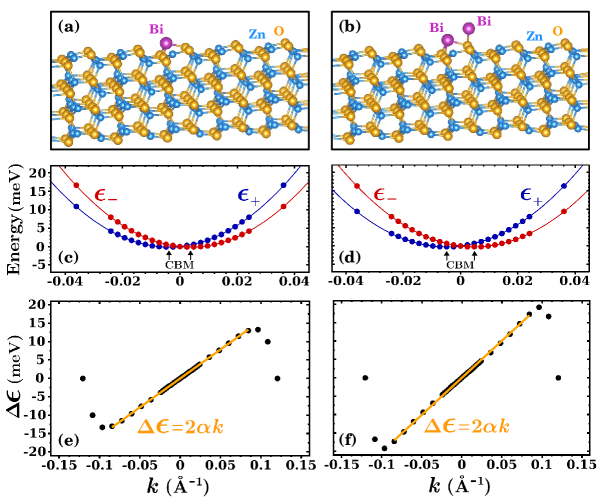
For the optimized atomic structures displayed in Figs. 1(a) and 1(b), viz. and , the SO-split conduction bands are shown in Figs. 1(c) and 1(d), respectively. It is seen that the dispersion of the these bands is accurately described by the solid curves (in blue and red) that represent fits in the form
| (1) |
which resembles the Bychkov-Rashba expressionBychkov and Rashba (1984). The values for the effective mass and the linear coefficient are given in Table 1 where the expectation values of the magnetization density corresponding to the bands are also given. Although these values appear to be small compared to the values of the Rashba parameter in “giant” Rashba systems such as Pt–Si nanowiresPark et al. (2013), it should be remarked that the SO splitting here is obtained by adding a single heavy atom to a light oxide, corresponding to a low (i.e., one Bi atom per 120 Zn–O pairs) concentration. This is appealing because enhancing spin-orbit coupling is usually accomplished by using significant amounts of heavy elements. The values in Table 1 are indeed of the same magnitude as the values in III-V heterostructuresNitta et al. (1997), making us expect Bi-doped ZnO nanowires find use in spintronic devices. The linear dependence of the band energies in the vicinity of the conduction band minimum (CBM) is further confirmed by plotting the splitting energy with respect to the wave vector in Figs. 1(e) and 1(f). The contribution from Bi to the states of the bands in Fig. 1(c) [Fig. 1(d)] is in the range of 3–4 % [6–7 %], cf. Fig. S1 (see Ref. sup, for Supplemental Material), showing that these bands are predominantly derived from the respective conduction bands of the host (ZnO) nanowire. Hence the states of the SO-split bands have more of character of extended states that facilitate (spin-polarized) electrical conduction.
Consider, for the purpose of interpretation, a Kramers doublet with two-component spinor wave functions and where denotes the wave function of the respective Bloch state in the absence of the SO interaction. The expectation value of the SO interaction operatorDavydov (1965) with can be expressed as
| (2) |
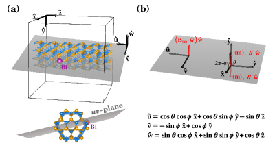
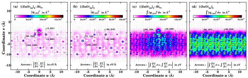
where is the -dependent matrix element of the operator (in the nonrelativistic limit). A similar equation follows for , but for our purpose it suffices to focus on . According to Eq. (2), a linear-in- SO splitting as in Eq. (1) occurs only if (i) is nonzero and (ii) has nonzero components in the direction parallel to . The condition (i) is satisfied for and as indicated by the values given in Table 1. In other words, the Bi incorporation leads to magnetization of the two lowest CB states although the total magnetic moment is zero for both and . It remains to see if the condition (ii) is also satisfied. It is convenient to use the coordinate system depicted in Figs. 2(a) and 2(b) where denotes the unit vector in the direction of . Because of the dot product in Eq. (2), we are interested only in the -component of that is perpendicular to the -plane, cf. Fig. 2(b). The latter, i.e., , involves and , and does not have any term with owing to the cross product in the definition of . In this line of reasoning, the origin of the SO splitting of the bands of , cf. Fig. 1(c), is sought by plotting the potential gradient on the plane in Fig. 3(a) where a colored contour plot of the state charge density is superimposed. Respective plots for the undoped nanowire are given in Fig. 3(b) for comparison. The arrows in Figs. 3(a) and 3(b) show the spatial inhomogeneity and asymmetry in the and components of the potential gradient, which gives rise to the effective field , and thus implies the satisfaction of the aforementioned condition (ii). The centrosymmetric pattern of arrows around the Bi atom in Fig. 3(a) should be noticed, indicating that the Bi atom would not make an appreciable contribution to . The inhomogeneity of the potential gradient is further characterized in Figs. 3(c) and 3(d) with the aid of integrated quantities (, ) and . A comparison of the arrows in Fig. 3(a) [Fig. 3(c)] with those in Fig. 3(b) [Fig. 3(d)] also indicates that the foregoing spatial inhomogeneity is not induced by the dopant. However, as will be elaborated in the Appendix, the incorporation of the dopant reduces the symmetry of the potential, rendering the CBM wave function to possess a lower symmetry. If the symmetry of the latter was conserved (i.e., remained the same as in the undoped ZnO nanowire), the matrix element in Eq. (2) would vanish, and no SO splitting could occur (which is clearly not the case). Nonetheless, the change in the potential gradient due to the dopant is small, as quantified in the Appendix. It can accordingly be said that the effective field originates mostly from the nonvanishing potential gradient of the host (ZnO) nanowire, owing to its noncentrosymmetric (wurtzite) structure. In sum, on one hand the donation of electrons of the Bi dopant leads to magnetization of the CB states, and on the other hand, the inhomogeneity of the potential gradient of the host nanowire gives rise to an effective SO field . Considering a Zeeman-type interaction, according to Eq. (2), between and the conduction electrons in the foregoing CB states explains the SO splitting of the bands shown in Figs. 1(c) and 1(d).
It is discernible in Figs. 3(a) and 3(c) that the CBM wave function is slightly localized in the regions close to the dopant, which has nevertheless comparable contributions from the dopant and host atoms. The latter precludes formation of a two-dimensional (2D) electron gas [although the lowest conduction bands in Fig. 1(c) are partially occupied], which means that the SO splitting in Bi-doped ZnO nanowire does not originate from the Rashba interactionBychkov and Rashba (1984). It should also be pointed out that the band splitting in Figs. 1(c) and 1(d) is not caused by the Dresselhaus effectDresselhaus (1955) since the Dresselhaus spin splitting does not occur along the direction in wurtzite semiconductorsDe and Pryor (2010) such as ZnOSchleife et al. (2009).
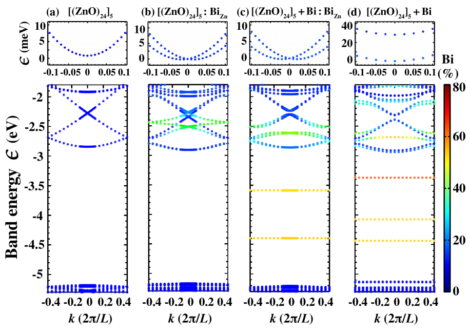
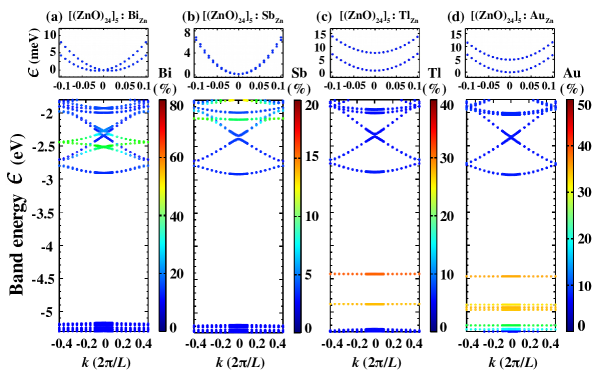
In order to see if doping a ZnO nanowire with elements other than Bi causes a spin splitting along the momentum axis as in Fig. 1(c), we repeated geometry optimizations and electronic structure calculations by replacing Bi with Tl, Au, or Sb. Figures 4(a)-4(d) display the electronic energy bands calculated for , , and , respectively, which are colored to reflect the percent contribution from the dopant (Bi, Sb, Tl, or Au) to the electronic states. The coloring is accomplished by computing the contributions from the dopant and host (Zn and O) atoms that are obtained by projecting the state wave functions onto spherical harmonics within a sphere around each atom. We see that the SO splitting in is virtually negligible, which is as anticipated because the SO effects are much less pronounced for a lighter (Sb) atom compared to a heavier (Bi) atom. We find in fact that the value of computed for is an order of magnitude smaller than the respective value for . On the other hand, doping with heavy elements Tl or Au results in a nonzero magnetic moment owing to formation of gap states with flat dispersion, cf. Figs. 4(c) and 4(d). Thus, the SO splitting of CBM in and occurs along the energy (as opposed to momentum) axis.
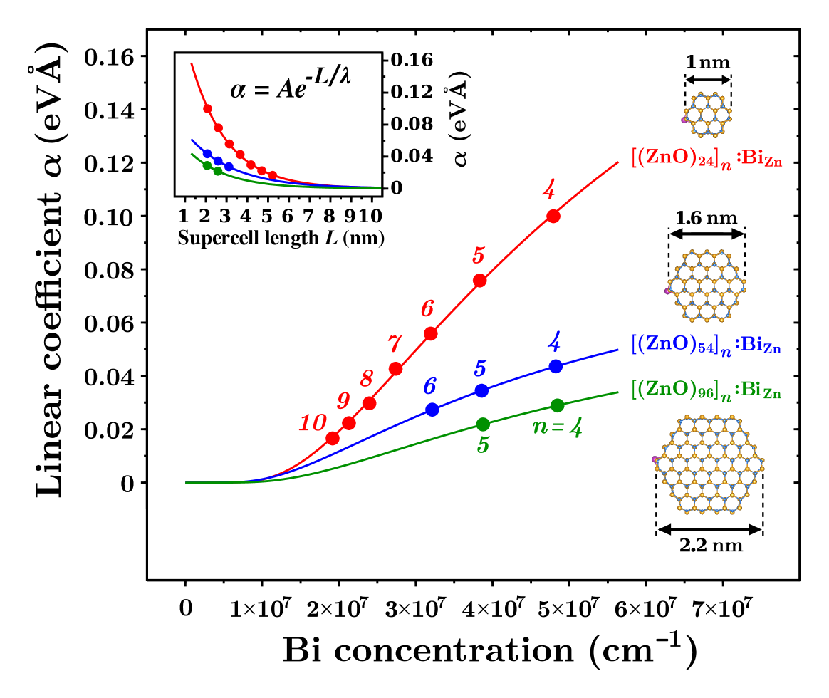
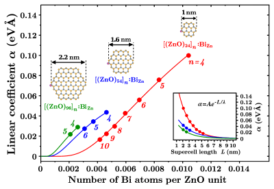
Figures 5 and S2 (see Ref. sup, for Supplemental Material) show the variation of the linear coefficient introduced in Eq. (1) with the Bi concentration for a set of host nanowires with increasing thicknesses corresponding to 24, 54, and 96. For each value of , a parameterization of as a function of the supercell length along the wire axis was performed, introducing two parameters and , which is shown in the inset of Fig. 5. The latter is used to plot versus the number of Bi atoms per ZnO unit [Fig. 5] and the Bi concentration in units of cm-1 [Fig. S2 (see Ref. sup, for Supplemental Material)]. We see that tends to reduce as the Bi concentration diminishes, which is in line with the fact that the linear-in- splitting does not occur in the absence of the dopant. Furthermore, the thicker the host nanowire the smaller the value in Fig. 5. It is thus clear that the value of , which manifests the degree of linear-in- splitting, could be tuned by adjusting the dopant concentration. The latter can be achieved by either decreasing the amount of the dopants (for a given ZnO nanowire) or increasing the number of Zn–O pairs, i.e., using a thicker nanowire. Consequently, doping-induced spin splitting in Bi-doped ZnO nanowires could be tuned and controlled by not only adjusting the amount of the dopants but also choosing a host nanowire of an adequate thickness.
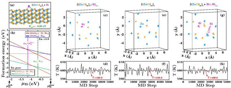
Bismuth has a low solubility in zinc oxide, which is known to give rise to the Bi segregation observed in ZnO varistorsSmith et al. (1989); Kobayashi et al. (1998). In accordance with this, our theoretical characterizationKılıç et al. (2016) of Bi-doped ZnO nanowires in a site-specific manner (as regards the location and charge-state of the dopant) showed that the dopant (Bi) atoms are predominantly substituted into the Zn sites on the nanowire surface. This implies that the doping configuration displayed in Fig. 1(a) would abound in the defect structure of Bi-doped ZnO nanowires. Here we employ defect calculations to see if the configurations displayed in Figs. 1(a) and 1(b) could be realized by putting the host nanowire into contact with a reservoir of bismuth. Thus, the formation energy of the Bi dopant in these configurations is plotted as a function of the Bi chemical potential in Fig. 6(b) under Zn–rich as well as Zn–poor conditions. The formation of an adsorbed Bi atom, denoted as , is also considered, for which the lowest-energy configuration is shown in Fig. 6(a). The values of corresponding to an equilibrium of the foregoing doping configurations with a reservoir consisting of (i) the Bi monomer gas, (ii) the Bi2 dimer gasZajaczkowski et al. (2016), (iii) the adsorbed Bi atoms, or (iv) the Bi solid are marked in Fig. 6(b). It is seen that the formation energies of and are both negative under Zn–poor (i.e., O–rich) conditions, regardless the bismuth reservoir. Hence these doping configurations can clearly be realized by putting the host nanowire into contact with an adequate reservoir of Bi under controlled thermodynamic conditions.
The stability of the foregoing doping configurations, cf. Figs. 1(a) and 1(b), is examined, in a relative manner, by performing ab initio MD simulations at temperature 600 K. The trajectories of atoms for , , and attained from the position of atoms (averaged over every 100 MD steps) are displayed in Figs. 6(c), 6(e), and 6(g), respectively. The respective graphs of the temperature (also averaged over every 100 MD steps) versus MD steps are given in Figs. 6(d), 6(f), and 6(h), which show that the temperature fluctuations are restricted to an interval of 20 K about the thermostat temperature K. The duration of our MD simulations is 5 ps (excluding the equilibration stage of 1 ps), which is likely shorter than needed for a complete prediction of the dynamical behavior of the studied systems. Nevertheless, it is clear from Figs. 6(c), 6(e), and 6(g) that not only the host (Zn, O) atoms but also the Bi dopant and adatom show a tendency to restore their equilibrium positions at a temperature (600 K) considerably higher than room temperature. Whereas the Bi adatom [Fig. 6(g)] has the greatest displacement, the Bi dopant [Fig. 6(c and g)] has the least displacement in comparison to the displacements of the host (Zn, O) atoms. This indicates that the Bi-doped ZnO nanowire is in fact as stable as the undoped ZnO nanowire, which is also supported by an overall comparison of the trajectory plots in Figs. 6(c) and 6(e). Furthermore, although our MD simulations were not intended to study the diffusion characteristics of Bi species on the surface of the ZnO nanowire, it is clear from Fig. 6(g) that the presence of the Bi adatom does not harm the stability of the substitutional Bi dopant.
IV Conclusion
The present investigation demonstrates that doping a semiconducting nanowire with a heavy element could be an effective means to lift Kramers degeneracy of the conduction-band states. In particular, doping ZnO nanowires with Bi is identified as a means to design quasi-one-dimensional materials for spintronic applications, thanks to the occurrence of the linear-in- spin-orbit splitting explored in this study. It is noteworthy that the degree of the linear-in- spin splitting, which would facilitate the control of spin-polarization of the conduction electrons in Bi-doped ZnO nanowires by applying external electric fields, could be tuned by adjusting the dopant concentration. Our findings suggest that Bi-doped ZnO nanowires, which are found to be stable under reasonable thermodynamic conditions, could be used in spintronic applications.
Acknowledgements.
The authors acknowledge financial support from TUBITAK through Grant 114F155. The numerical calculations reported here were carried out at the High Performance and Grid Computing Center (TRUBA Resources) of TUBITAK ULAKBIM.*
Appendix A Lowering of the symmetry in the presence of the dopant
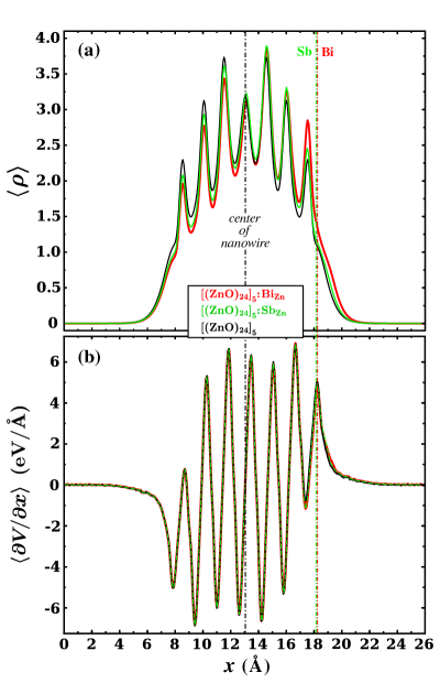
From the perspective of symmetry, the linear-in- SO splitting in Eq. (1) cannot be attributed to the host (ZnO) nanowire. Since the irreducible representations of C compatible with spin are doubly-degenerate, no spin splitting occurs along the -A direction of the wurtzite Brillouin zoneLew Yan Voon et al. (1996). This is also valid for the ZnO nanowires employed here, whose point group is C, in the absence of the Bi dopant, cf. Fig. S1(a) (see Ref. sup, for Supplemental Material). It is thus clear that the SO splitting explored here occurs due to lowering of the symmetry in the presence of the dopant. Here we present an analysis of the latter in terms of doping-induced changes in the potential gradient and the CBM wave function since the expectation value of the SO interaction operator involves both, cf. Eq. (2). This analysis is conducted by plotting the planar average of the state charge density in Fig. 7(a) and the potential gradient in Fig. 7(b) with respect to , where is set as the wave vector at which the CBM occurs. It is instructive to compare the Bi-doped nanowire to not only the undoped nanowire but also the Sb-doped nanowire because and possess the same symmetry. As respectively seen in Figs. 7(a) and 7(b), both and have asymmetric profiles in the presence of the dopant (Bi or Sb), which could be explained by noting that the reflection symmetry with the mirror plane at the center of the nanowire is lost when the dopant is incorporated. It is also seen that the doping-induced change in is not noteworthy whereas the change in shows a significantly asymmetric profile, as will be quantified in the next paragraph. Comparing the curves for and in Fig. 7(b) to each other, it is seen that the change in the potential gradient is quite indifferent to the type of dopant, which is seemingly not the case with the state charge density since the red curve, in comparison to the green curve, is in a larger deviation from the black (symmetric) curve in Fig. 7(a). These comparisons show that the essential difference between doping with Bi and Sb pertains mostly to the change in the CBM wave function, rather than the potential gradient. This means that reducing the symmetry of would not necessarily produce a SO splitting as in Eq. (1); it must be accompanied by the adequate modification of the state wave function to a lower symmetry, cf. Fig. 7(a), as in the case of .
The lowering of the symmetry in the presence of the dopant (Bi or Sb) can be quantified by introducing the following quantities: , , , and , where and , and and [ and ] denote the state charge density and potential of the doped [undoped] nanowire. Note that (i) ; the computed value of eV for is half of that for for which eV. (ii) involves only the host-related quantities, and so owing to the symmetry of the undoped ZnO nanowire. (iii) and are “measures” of the degree of doping-induced asymmetry due to the change in the potential and in the state charge density, respectively. We obtain eV for both and whereas and 0.11 eV for and ,respectively. Note that take the same value for both dopants, which is significantly smaller than the respective values. This means that the doping-induced asymmetry due to the changes in the state wave function, rather than in the potential gradient, is pronounced. Accordingly, what really differentiates the cases of doping Bi versus Sb is the lowering of the symmetry of the CBM wave function.
References
- Moroz and Barnes (1999) A. V. Moroz and C. H. W. Barnes, Phys. Rev. B 60, 14272 (1999).
- Zhang et al. (2006) S. Zhang, R. Liang, E. Zhang, L. Zhang, and Y. Liu, Phys. Rev. B 73, 155316 (2006).
- Pramanik et al. (2007) S. Pramanik, S. Bandyopadhyay, and M. Cahay, Phys. Rev. B 76, 155325 (2007).
- Quay et al. (2010) C. Quay, T. Hughes, J. Sulpizio, L. Pfeiffer, K. Baldwin, K. West, D. Goldhaber-Gordon, and R. De Picciotto, Nature Physics 6, 336 (2010).
- Luo et al. (2011) J.-W. Luo, L. Zhang, and A. Zunger, Phys. Rev. B 84, 121303 (2011).
- Crepaldi et al. (2013) A. Crepaldi, G. Bihlmayer, K. Kern, and M. Grioni, New J. Phys. 15, 105013 (2013).
- Park et al. (2013) J. Park, S. W. Jung, M.-C. Jung, H. Yamane, N. Kosugi, and H. W. Yeom, Phys. Rev. Lett. 110, 036801 (2013).
- Hsu and Chang (2014) C.-L. Hsu and S.-J. Chang, Small 10, 4562 (2014).
- Li et al. (2013) G. Li, A. Sundararajan, A. Mouti, Y.-J. Chang, A. R. Lupini, S. J. Pennycook, D. R. Strachan, and B. S. Guiton, Nanoscale 5, 2259 (2013).
- Spencer (2012) M. J. Spencer, Prog. Mater Sci. 57, 437 (2012).
- Lupan et al. (2011) O. Lupan, T. Pauport, T. Le Bahers, B. Viana, and I. Ciofini, Adv. Funct. Mater. 21, 3564 (2011).
- Lu et al. (2009) M.-P. Lu, J. Song, M.-Y. Lu, M.-T. Chen, Y. Gao, L.-J. Chen, and Z. L. Wang, Nano Lett. 9, 1223 (2009).
- Yuan et al. (2008) G.-D. Yuan, W.-J. Zhang, J.-S. Jie, X. Fan, J.-X. Tang, I. Shafiq, Z.-Z. Ye, C.-S. Lee, and S.-T. Lee, Adv. Mater. 20, 168 (2008).
- Huang et al. (2007) Y. Huang, Y. Zhang, Y. Gu, X. Bai, J. Qi, Q. Liao, and J. Liu, J. Phys. Chem. C 111, 9039 (2007).
- Chang et al. (2003) Y. Q. Chang, D. B. Wang, X. H. Luo, X. Y. Xu, X. H. Chen, L. Li, C. P. Chen, R. M. Wang, J. Xu, and D. P. Yu, Appl. Phys. Lett. 83, 4020-4022 (2003).
- Cui and Gibson (2005) J. B. Cui and U. J. Gibson, Appl. Phys. Lett. 87, 133108 (2005).
- Segura-Ruiz et al. (2011) J. Segura-Ruiz, G. Martínez-Criado, M. H. Chu, S. Geburt, and C. Ronning, Nano Lett. 11, 5322 (2011).
- Iqbal et al. (2009) J. Iqbal, X. Liu, H. Zhu, C. Pan, Y. Zhang, D. Yu, and R. Yu, J. Appl. Phys. 106, 083515 (2009).
- Ma (2012) X. Ma, Thin Solid Films 520, 5752 (2012).
- Hoffmann and Bader (2015) A. Hoffmann and S. D. Bader, Phys. Rev. Applied 4, 047001 (2015).
- Xu et al. (2007) C. Xu, J. Chun, D. E. Kim, J.-J. Kim, B. Chon, and T. Joo, Appl. Phys. Lett. 90, 083113 (2007).
- Kılıç et al. (2016) Ç. Kılıç, M. Aras, and S. Güler-Kılıç, “Computational studies of bismuth-doped zinc oxide nanowires,” in Low-Dimensional and Nanostructured Materials and Devices: Properties, Synthesis, Characterization, Modelling and Applications, edited by H. Ünlü, M. N. J. Horing, and J. Dabowski (Springer International Publishing, Cham, 2016) pp. 401–421.
- Xiu et al. (2006) F. X. Xiu, L. J. Mandalapu, Z. Yang, J. L. Liu, G. F. Liu, and J. A. Yarmoff, Appl. Phys. Lett. 89, 052103 (2006).
- Smith et al. (1989) A. Smith, J. Baumard, P. Ab lard, and M. Denanot, J. Appl. Phys. 65, 5119-5125 (1989).
- Silsbee (2004) R. H. Silsbee, J. Phys.: Condens. Matter 16, R179 (2004).
- Dresselhaus (1955) G. Dresselhaus, Phys. Rev. 100, 580 (1955).
- Bychkov and Rashba (1984) Y. A. Bychkov and E. Rashba, JETP Lett 39, 78 (1984).
- G. Kresse and J. Furthmüller (1996) G. Kresse and J. Furthmüller, Phys. Rev. B 54, 11169 (1996).
- Dudarev et al. (1998) S. L. Dudarev, G. A. Botton, S. Y. Savrasov, C. J. Humphreys, and A. P. Sutton, Phys. Rev. B 57, 1505 (1998).
- Perdew et al. (1996) J. P. Perdew, K. Burke, and M. Ernzerhof, Phys. Rev. Lett. 77, 3865 (1996).
- P. E. Blöchl (1994) P. E. Blöchl, Phys. Rev. B 50, 17953 (1994).
- Kresse and Joubert (1999) G. Kresse and D. Joubert, Phys. Rev. B 59, 1758 (1999).
- Aras and Ç. Kılıç (2014) M. Aras and Ç. Kılıç, J. Chem. Phys. 141, 044106 (2014).
- Hobbs et al. (2000) D. Hobbs, G. Kresse, and J. Hafner, Phys. Rev. B 62, 11556 (2000).
- Marsman and Hafner (2002) M. Marsman and J. Hafner, Phys. Rev. B 66, 224409 (2002).
- Nosé (1984) S. Nosé, J. Chem. Phys. 81 (1984).
- Tronc et al. (2006) P. Tronc, V. Stevanovic, I. Milosevic, and M. Damnjanovic, phys. stat. sol. (b) 243, 1750 (2006).
- Nitta et al. (1997) J. Nitta, T. Akazaki, H. Takayanagi, and T. Enoki, Phys. Rev. Lett. 78, 1335 (1997).
- (39) See Supplemental Material for Fig. S1 that displays the electronic energy bands calculated for , , , , which are colored according to the contribution of atoms, and Fig. S2 that shows the plot of the linear coefficient versus the Bi concentration in units of cm-1.
- Davydov (1965) A. Davydov, Quantum mechanics, 1st ed. (Pergamon Press, 1965) p. 252.
- De and Pryor (2010) A. De and C. E. Pryor, Phys. Rev. B 81, 155210 (2010).
- Schleife et al. (2009) A. Schleife, F. Fuchs, C. Rödl, J. Furthmüller, and F. Bechstedt, Phys. Status Solidi B 246, 2150 (2009).
- Kobayashi et al. (1998) K.-I. Kobayashi, O. Wada, M. Kobayashi, and Y. Takada, J. Am. Ceram. Soc. 81, 2071 (1998).
- Zajaczkowski et al. (2016) A. Zajaczkowski, J. Czernecki, and A. Surulo, Calphad 52, 66 (2016).
- Lew Yan Voon et al. (1996) L. C. Lew Yan Voon, M. Willatzen, M. Cardona, and N. E. Christensen, Phys. Rev. B 53, 10703 (1996).
Supplemental Material
-
•
Figure S1 displays the electronic energy bands calculated for , , , , which are colored according to the contribution of atoms.
-
•
Figure S2 shows the plot of the linear coefficient versus the Bi concentration in units of cm-1.