Microanalysis of single-layer hexagonal boron nitride islands on Ir(111)
Abstract
Large hexagonal boron nitride (hBN) single-layer islands of high crystalline quality were grown on Ir(111) via chemical vapor deposition (CVD) and have been studied with low-energy electron microscopy (LEEM). Two types of hBN islands have been observed that structurally differ in their shape and orientation with respect to iridium, where the former greatly depends on the iridium step morphology. Photoemission electron microscopy (PEEM) and IV-LEEM spectroscopy revealed that the two island types also exhibit different work functions and bindings to iridium, which provides an explanation for differences in their shape and growth modes. In addition, various temperatures were used for the CVD synthesis of hBN, and it was found that at temperatures higher than °C boron atoms, originating either from decomposed borazine molecules or disintegrated hBN islands, can form additional compact reconstructed regions. The presented results are important for advancement in synthesis of high-quality hBN and other boron-based layered materials, and could therefore expedite their technological implementation.
I Introduction
Alongside pioneering graphene (G), researchers have characterized a large number of other two-dimensional (2D) materials Xu et al. (2013) that may potentially be used in novel applications. Among them, single-layer hexagonal boron nitride (hBN) is particularly interesting due to the isostructurality to G Pakdel et al. (2014) and its insulating nature, i.e., a large bandgap of eV Cassabois et al. (2016). These properties, alongside with atomic flatness, chemical inertness and the absence of charge traps, designate hBN as a very important 2D material, ideal for the formation of heterostructures with G that promise various technological advancements, for example, in transistor Dean et al. (2010); Bresnehan et al. (2012) or integrated circuits Levendorf et al. (2012) fabrication. Besides in combination with graphene, hBN may be used for encapsulation of other 2D materials which enhances their performance in various devices Lee et al. (2015). Furthermore, other applications of hBN include use as an active laser medium Watanabe et al. (2004) and an ultra-thin insulating support for molecular self-assembly Corso et al. (2004); Schulz et al. (2013).
Single layers of hBN can be produced via chemical vapor deposition (CVD) on various single-crystal metal substrates Auwärter et al. (1999); Morscher et al. (2006); Goriachko et al. (2007); Ćavar et al. (2008); Dong et al. (2010); Müller et al. (2010); Orlando et al. (2012); Joshi et al. (2012). Similar to the case of epitaxial G Wintterlin and Bocquet (2009); Celasco et al. (2017), some metals are characterized by strong interaction with hBN, such as Ru(0001) or Rh(111), while on other substrates hBN is more weakly bound, e.g., on Pt(111) or Cu(111) Preobrajenski et al. (2005, 2007a); Laskowski and Blaha (2010). Optimal hBN production requires a substrate to which, on the one hand, hBN binds sufficiently strongly to enable the growth of uniformly oriented domains and on the other hand, does not bind too strongly in order to preserve its intrinsic properties. These requirements are fulfilled for hBN on Ir(111) [hBN/Ir(111)] because there the interaction is characterized as intermediate Preobrajenski et al. (2007b); Laskowski et al. (2008). Moreover, high-quality G samples with preserved intrinsic electronic structure are easily synthesized on Ir(111) Kralj et al. (2011) and are a very good starting point for the fabrication of G-based heterostructures. Therefore, Ir(111) is a suitable substrate for studying both fundamental properties of hBN as well as more complex systems comprised of hBN and other 2D materials.
A number of studies of hBN/Ir(111) have been conducted so far, but there are still aspects of the system that require further investigation. For example, hBN exhibits two preferential orientations with respect to Ir(111) which were identified via X-ray photoelectron diffraction (XPD) Orlando et al. (2014) and scanning tunneling microscopy (STM) Farwick zum Hagen et al. (2016), but a more detailed morphological characterization of the respective hBN domains is lacking, especially on the micro-scale. Also, differences in the electronic structure of the two hBN orientations are not known, since only area-averaging ARPES has been performed for valence band mapping Usachov et al. (2012). In addition, the above mentioned studies report on the decomposition of hBN at elevated temperatures and emergence of other boron species on the iridium surface, as evidenced by STM imaging Farwick zum Hagen et al. (2016) as well as disappearance and appearance of different B 1s peaks in XPS Usachov et al. (2012). Details of these processes, which are vital for establishment of high-quality hBN synthesis, are not known. Moreover, insight into formation of various boron structures could initiate the production of borophene–an exciting 2D boron analogue of G Mannix et al. (2015)–on iridium. To investigate all these issues, the use of a complementary microscopic technique is necessary. Low-energy electron microscopy (LEEM) is an ideal tool for this task because it enables in situ, real-time observation of growth-related phenomena with the spatial resolution in the nanometer range. With this method, hBN has been characterized on e.g., Pt(111) Ćavar et al. (2008); Zhang et al. (2015), Ru(0001) Goriachko et al. (2008); Sutter et al. (2011) and Co(0001) Orofeo et al. (2013), but similar studies addressing hBN/Ir(111) are still lacking. The aim of this work is to provide first microscopic insights into this epitaxial system primarily via LEEM and in conjunction with several other methods, which will supplement our findings. In this way we tackle challenges of CVD synthesis of hBN, which is the most promising technique for the large-scale production of hBN.
II Experimental
Growth of hBN was conducted in an ultra-high vacuum (UHV) setup with a base pressure better than mbar. CVD was used for the synthesis of hBN during which a hot (111) surface of Ir single-crystal (Mateck) was exposed to borazine (B3H6N3, Katchem). The crystal was cleaned by Ar+ sputtering at 2 keV followed by several cycles of heating in oxygen at 900 °C and annealing at 1200 °C. In the case when only hBN had to be removed from the surface, heating in oxygen and annealing were sufficient. The sample temperature was measured with an infrared pyrometer. Borazine was kept in a home-built Peltier cooler, which enabled realization of the sub-zero temperatures needed to prevent borazine decomposition. Thus, borazine was available at all times at the UHV setup, and prior to each hBN synthesis the borazine inlet line was pumped down to remove any decomposition residues. Unless otherwise noted, borazine pressure during CVD was mbar.
LEEM and PEEM measurements were carried out in situ with an Elmitec SPE-LEEM III microscope at the University of Duisburg-Essen. PEEM measurements were performed with the aid of an Hg discharge lamp providing eV photons that were relevant for our samples. The spatial resolution of the microscope is nm. Atomic force microscope (AFM) measurements were performed ex situ in air with a Veeco Dimension 3100 microscope operated in tapping mode. An Auger Nanoprobe 710 from Ulvac-Phi located at the ICAN center in Duisburg was used for ex situ Auger electron spectroscopy (AES) and scanning electron microscopy (SEM) with a base pressure of mbar. Primary electron energy for AES was 10 keV and 5 keV for SEM.
III Results and discussion
III.1 Temperature-dependent growth
In order to investigate different growth conditions, hBN islands were synthesized at various temperatures in LEEM. Fig. 1(a)-(c) show characteristic island morphologies for the growth temperatures of 800, 900 and 1100 °C (note that fields of view are not the same in all panels). In all cases, island nucleation was initiated at Ir step edges. At low synthesis temperatures, this resulted in the formation of strings of hBN islands that decorate the same Ir step edge, as marked in Fig. 1(a) with a yellow rectangle. The corresponding island densities in Fig. 1(a)-(c) are 8.09, 0.58 and 0.02 μm-2, thus spanning several orders of magnitude. At the same time, the average island size increases with synthesis temperature. These findings are in line with published STM data of hBN synthesized at different temperatures Farwick zum Hagen et al. (2016) and the temperature- and dose-dependence of the classical nucleation theory in general. With the growth conditions we used, hBN islands with sizes up to μm (for 1100 °C synthesis) were readily obtained. During prolonged exposure to borazine, individual islands coalesce, resulting in a full coverage of hBN and suppression of multilayer growth, similar to hBN growth on Ru(0001) Sutter et al. (2011).
Upon cooldown to room temperature, the formation of wrinkles was not observed on either islands or a full hBN monolayer [see Fig. 4(a) or (d) as an example]. However, wrinkling was found before for hBN on weakly interacting substrates, such as Pt(111) Zhang et al. (2015) or Cu foils Kim et al. (2012). In contrast to hBN, G wrinkles on Ir(111) are routinely observed via LEEM and have been characterized in detail N’Diaye et al. (2009); Petrović et al. (2015). Therefore, our data indicates that wrinkling does not occur on hBN/Ir(111). This suggests that (i) the binding of hBN and G to Ir is different and/or that (ii) the elastic stiffness of hBN is lower than that of G. In comparison, theoretical calculations give binding strength to Ir of 138 meV per G and 170.8 meV per hBN unit cell Farwick zum Hagen et al. (2016). Also, AFM indentation experiments of suspended layers provided an elastic stiffness value of 340 Nm-1 for G Lee et al. (2008) and, in combination with theoretical modeling, 292 Nm-1 for hBN Song et al. (2010). Because binding and stiffness values are comparably close, it seems that a combination of both contributes to the absence of wrinkle formation in hBN.
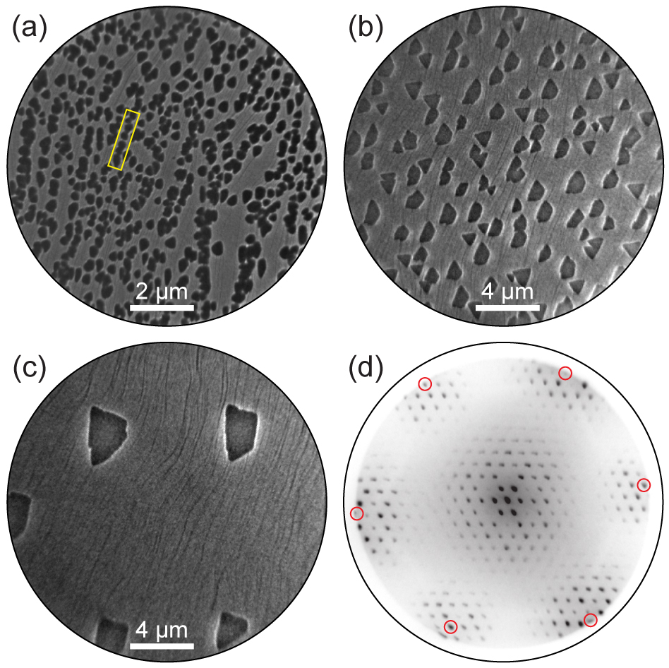
A characteristic low-energy electron diffraction (LEED) pattern of several coalescing hBN islands synthesized at 900 °C is shown in Fig. 1(d). The most prominent features of the pattern are diffraction spots that reflect the presence of the moiré structure of hBN/Ir(111) arising from the mismatch of the two surface lattices. The high quality of our hBN islands is confirmed by a large number of sharp moiré spots, which range up to the sixth order and thus span almost the entire first Brillouin zone. A closer look at the diffraction spots in Fig. 1(d) reveals that the hBN area under examination consists of several slightly rotated domains (see Subsection 3.2. for details on rotational registry of hBN and Ir). From a more detailed analysis of similar LEED patterns, we calculate the ratio of hBN and Ir reciprocal lattice vector modules, , to be . Hence, the structure of hBN on Ir is such that unit cells of hBN are superposed on top of 10 unit cells of Ir. The calculated ratio of 1.09 matches the ratio of (and also as the best commensurate approximation), which was recently reported as an exact description of the hBN/Ir(111) moiré structure Farwick zum Hagen et al. (2016). Knowing that the Ir real space lattice constant is Å Arblaster (2010), we calculate the lattice constant of hBN to be Å, which is in good agreement with the published values for hBN/Ir(111) of 2.483 Å Farwick zum Hagen et al. (2016) as well as that for bulk hBN of 2.505 Å Paszkowicz et al. (2002). Also, the ratio enables calculation of the corresponding moiré periodicity, which turns out to be Å (for the hBN aligned to Ir), being consistent with the reported STM measurements Schulz et al. (2014); Farwick zum Hagen et al. (2016).
The stability of hBN islands was examined by keeping the sample at high temperatures after stopping the borazine dosage. It was found that in the case of sufficiently high temperatures, synthesized hBN islands disintegrate from the perimeter inward and eventually vanish from the field of view. An example of disintegration is shown in a sequence of LEEM images in Fig. 2(a) for the sample temperature of 1100 °C. There are two possible routes for the B and N atoms after an hBN island decomposes: the atoms can desorb from the sample or they can remain on the Ir surface, either in the adsorbed or dissolved form. N desorption and B dissolution into the bulk seem to be the most probable scenario because N2 molecules desorb from the (111) surface of Ir even below room temperature Cornish and Avery (1990), while iridium borides of various stoichiometric ratios can be formed at high temperatures Zeiringer et al. (2015). Further experiments corroborating this assumption are described in the following.
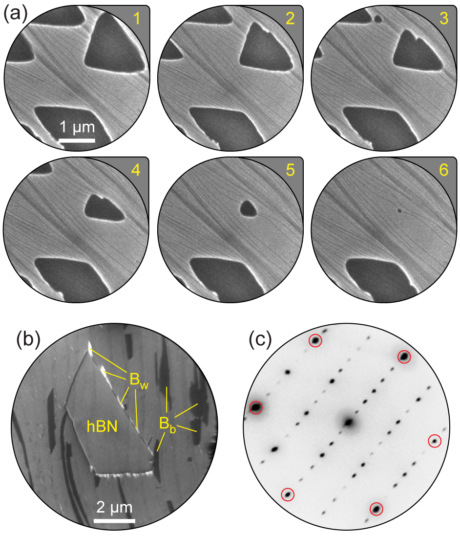
Fig. 2(b) shows the surface of the sample after hBN synthesis at 1100 °C and subsequent cooldown to room temperature. Beside a compact hBN island, extra material is visible in the form of dark, elongated features that predominantly follow the shape of Ir step edges, and irregular bright patches that decorate hBN island edges. We label this additional material as Bb and Bw, respectively. Bb regions appeared during cooldown at °C, and they were also observed if cooldown was performed before any hBN nucleation or after hBN disintegration. We noticed that Bw regions grew if the sample was kept at elevated synthesis temperature without dosing borazine and the hBN island they grew attached to remained unaltered. All this evidence suggests that the Bb and Bw regions are in fact reconstructed boron areas. B atoms are fed to those regions from the borazine gas phase and from disintegrated hBN islands, while the mechanism of Bb and Bw formation is either (i) diffusion of B atoms across the Ir surface and eventual nucleation or (ii) dissolution of B atoms into Ir subsurface regions followed by segregation due to the decrease of solubility at lower temperatures. Therefore, the threshold temperature for significant disintegration of hBN on (111) face of Ir and the diffusion of B into the subsurface regions is °C, and a slightly lower temperature (900 °C) was used for synthesis when hBN islands without excessive B regions surrounding them were desired. μ-LEED analysis, enabling diffraction studies of sub-micrometer-sized areas on the sample surface, revealed that Bb regions exhibit an adsorbate (not adlayer) form due to the relatively dilute superstructure [see the diffraction pattern in Fig. 2(c)], and they were present on the surface in three equivalent 120°-rotated variants. Bw regions exhibit a (or possibly disordered) structure (not shown). We also note that Bb and Bw regions are easily etched away at elevated temperatures with oxygen.
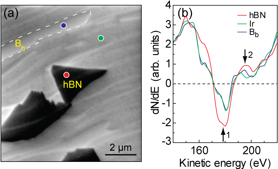
In order to confirm our speculations on the chemical composition of Bb and Bw regions, AES was performed. A suitable area for AES was first found with SEM and is shown in Fig. 3(a). hBN islands appear dark and Bb regions are visible as elongated, slightly lighter structures when compared with the surrounding bare Ir. The mode of contrast generation in SEM (which is different to the one in LEEM) does not enable imaging of the small Bw regions attached to hBN. Because of this, Bw regions were not accessible for Auger analysis. Three characteristic positions (bare Ir, hBN and Bb) marked by colored dots (green, red and blue, respectively) were chosen and the resulting AES spectra are shown in Fig. 3(b), with a focus on the energy range where the main B peak is expected to be found Sutter and Sutter (2014). A notable Ir peak is located in the same region and contributes to all recorded Auger spectra, which hinders our analysis. A larger peak of the hBN spectrum (red curve) as compared with the bare Ir spectrum (green curve) in the region indicated by arrow 1 is ascribed to the presence of B in hBN. The excess of B can also be read out from the hBN spectrum peak in the area indicated by arrow 2. The Auger spectrum of Bb (blue curve) is more similar to bare Ir spectrum, and the two spectra are in principle indistinguishable in the region of arrow 1. However, a difference between them is found in the region of arrow 2 where the discernible peak of the Bb region is visible. Although small, this difference between bare Ir and Bb spectra was systematically found for different sets of spectra, and we therefore ascribe it to the presence of B in Bb regions. One should keep in mind the concentration of B within the Bb: it is approximately of the concentration within the hBN island (under the assumption of one B atom per Bb unit cell), thus diminishing the intensity of the B Auger peaks by the same factor.
The disintegration of hBN and the presence of additional B species on the surface is complemented by several published studies of hBN/Ir(111). From their XPS results, Usachov et al. found that B 1s and N 1s spectra intensities decrease rapidly if the sample is kept at temperatures higher than 1000 °C Usachov et al. (2012), ascribing this to hBN decomposition accompanied by N desorbtion and B diffusion to the Ir subsurface regions. Moreover, the authors find, besides the main peak assigned to hBN, two additional B peaks that signify the existence of two additional forms of boron. In the same study, LEED images indicate a superstructure in addition to the moiré diffraction spots, which is evidence for the presence of Bb islands. Farwick zum Hagen et al. provided an atomistic view of Bw islands via STM that exhibit a structure Farwick zum Hagen et al. (2016). There, the existence of Bw islands was ascribed to the decomposition of hBN because the authors observed a similar structure in the inner parts of hBN islands. Therefore, the process of hBN disintegration as well as the formation of different B structures on the Ir surface has been evidenced by several experimental techniques and should be taken into account for optimal hBN synthesis, and considered as initial steps towards potential synthesis of borophene on iridium.
III.2 Island shape and alignment with iridium
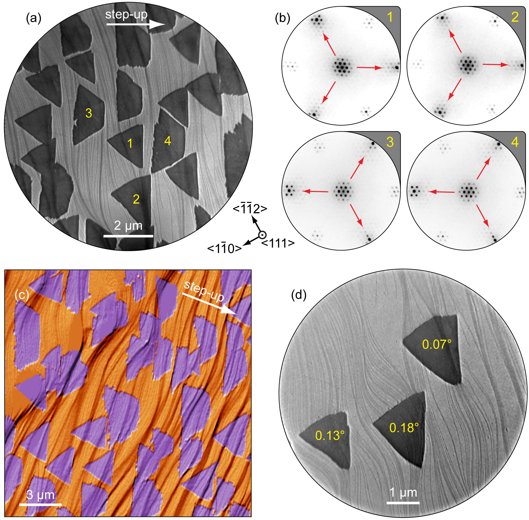
We now turn to a more detailed analysis of individual hBN islands. After a CVD synthesis at 900 °C, two basic island shapes were found on Ir surface: triangular and trapezoidal, as shown in Fig. 4(a). This is particularly the case in the initial stages of growth when the islands are small and their shape (i.e., edge straightness and angles between the edges) is not much affected by the Ir step morphology. Typical island size ranges from 1 to 2 μm and sides of neighboring triangles and trapezoids are parallel or nearly parallel, indicating alignment with respect to the substrate and the existence of a preferred edge type. The island densities of both triangular and trapezoidal islands were roughly equal. Moreover, the two island types are rotated by 180° with respect to each other, as is inferred from their diffraction patterns shown in Fig. 4(b).
High-symmetry crystal directions, which are easily determined in LEED, can be mapped to real-space directions in LEEM images, and this allows for the determination of the hBN island edge type. It is found that all edges (for both triangles and trapezoids) are of the zig-zag (ZZ) type under the assumption that no edge reconstruction takes place (as has been proposed theoretically for hBN on metals Zhang et al. (2016)). Indeed, the ZZ edge type has also been confirmed in STM experiments, and boron-termination has been suggested based on the DFT calculations Liu et al. (2014); Farwick zum Hagen et al. (2016). Deviations from ZZ edges occur when islands grow bigger and initial straight edges, mutually connected at 60° or 120°, are lost. The mere observation of triangular island shapes also suggests a ZZ edge type because ZZ edge configuration in hexagonal 2D materials with bi-elemental basis enables the presence of one atomic species on the edge, the one which provides an edge of lower energy. In the case of G growth, initial small islands are often hexagonal because of mono-elemental basis.
The existence of two 180°-rotated variants of hBN islands on Ir(111) was reported before, including the synthesis recipe enabling prevalence of one orientation over the other Orlando et al. (2014); Farwick zum Hagen et al. (2016). Also, triangular islands of two orientations have been reported for hBN on strongly interacting substrates such as Ni(111) Auwärter et al. (2003), Rh(111) Dong et al. (2010), Ru(0001) Lu et al. (2013) and Co(0001) Orofeo et al. (2013). Theoretical calculations for systems without the moiré structure showed that the two orientations stem from the two possible stable configurations of hBN on metals Grad et al. (2003); Laskowski et al. (2008). In both of them, N atoms are located on top of the Ir atoms (Ntop), while B atoms can be either in the hcp (Bhcp) of fcc (Bfcc) sites, leading to the formation of two 180°-rotated domains. However, for systems that develop the moiré structure, such as hBN/Ir(111), the registry between N and B atoms with respect to Ir atoms changes across the moiré unit cell. But even in such cases, two 180°-rotated orientations of the hBN layer are preferred, especially if island edge interaction with the substrate is considered to be dominant in total binding Camilli et al. (2014); Farwick zum Hagen et al. (2016).
One of our AFM measurements is shown in Fig. 4(c) where individual triangular and trapezoidal hBN islands as well as Ir steps are visible. The short base of the trapezoidal island always forms in the step-up direction of Ir. It should be noted that because the trapezoidal islands have two ZZ edges that are parallel, they must contain different types of edge atoms. Therefore, trapezoidal islands form a ZZ edge of the opposite composition in the step-up direction as compared with all other edges. Because this behavior is absent for triangular islands, we speculate that it is a result of an energetic balance between the two ZZ edge types (N- and B-terminated) and different interaction of the two island types with the substrate, in particular with the substrate step edges. Indeed, STM measurements Farwick zum Hagen et al. (2016) have shown that both island types are triangular in the initial phases of growth when their dimensions do not exceed typical Ir terrace widths, indicating the importance of Ir steps for the overall island shape. The issue of the binding of hBN islands to Ir will be addressed in more detail in the next section.
The rotational registry of hBN islands synthesized at 900 °C was investigated by μ-LEED analysis. With the aid of the moiré structure, relative rotations of hexagonal 2D overlayers with respect to Ir are effectively magnified N’Diaye et al. (2008) and can therefore be determined with high precision. For hBN on Ir(111), this magnification is times, as can be calculated from the lattice constant values given in Subsection 3.1. By scanning over many islands, small rotations in the sub-degree region were found. An example is given in Fig. 4(d) for three neighboring islands exhibiting small rotations (0° is defined as an alignment of hBN ZZ direction and dense packed atomic rows of Ir). A small angle misalignment between hBN and Ir lattices was reported before for hBN/Ir(111) Schulz et al. (2014); Farwick zum Hagen et al. (2016) and is also known to be present in G on Ir(111) N’Diaye et al. (2008); Coraux et al. (2008). The major factor influencing orientational quality of both 2D materials is the synthesis temperature Hattab et al. (2011); Usachov et al. (2012), and in our case it could be improved at the expense of the Bb and Bw regions formation.
III.3 Work function and interaction with iridium
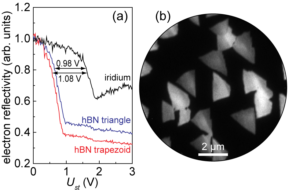
Basic information about the electronic structure of the triangular and trapezoidal islands was obtained from the combination of IV-LEEM spectroscopy and PEEM. In Fig. 5(a), three normalized bright field IV-LEEM spectra taken from bare Ir and the two hBN island types are shown. By looking at the drop in electron reflectivity when increasing the electron energy, it is obvious that the examined areas have different work functions (WFs) Babout et al. (1980). We estimate the difference in the WF between Ir and triangular hBN island to be 0.98 eV, while it is larger for the trapezoidal island and amounts to 1.08 eV. In other words, trapezoidal islands exhibit a WF that is 0.1 eV lower that the WF of triangular islands. These values were obtained by performing a linear fit to the reflectivity shoulders and then determining their relative offsets at a reflectivity value of 0.8. By taking the WF of bare Ir to be 5.76 eV Strayer et al. (1973), hBN triangles and trapezoids have WFs of 4.78 and 4.68 eV, respectively.
These values are somewhat lower that the ones reported in an spectroscopy study of hBN/Ir(111) by Schultz et al. Schulz et al. (2014). In the same work, the authors showed that more strongly interacting areas of the hBN/Ir(111) moiré cell exhibit larger WF. Similarly, from IV-LEEM measurements of G on Ir(111), Starodub et al. Starodub et al. (2011) found that more strongly bound rotational variant of G has a higher WF. Therefore, we speculate that of the two hBN island types, triangular ones are more strongly bound to Ir. A difference in binding strength, although amounting only to 2.8 meV per hBN unit cell, has also been suggested based on the DFT calculations Farwick zum Hagen et al. (2016).
The binding inequivalence speculation is further supported by a PEEM measurement shown in Fig. 5(b). It demonstrates that triangular and trapezoidal islands exhibit different photoemission intensities, which in fact reflect differences in the electronic structure of the hBN/Ir(111) system as a whole. The first factor that can contribute to this difference is the WF variation. The second factor to be considered is the coherence of the Ir surface state at the point Niesner et al. (2012), which is the most probable source of photoelectrons in PEEM images, because it remains present on the surface after hBN formation Usachov et al. (2012). A strong hBN-Ir interaction can potentially cause quenching of the surface state Schulz et al. (2014), which would reduce the photoemission yield in PEEM. Therefore, both IV-LEEM and PEEM measurements suggest stronger interaction of the triangular hBN islands with Ir, as opposed to the trapezoidal ones. Overall, different binding of the two island types could be the source of different growth modes and consequently, in combination with substrate morphology, different island shapes. Trapezoidal islands have been observed for hBN on Pt(111) where binding to the substrate is weak, but their origin was not discussed Zhang et al. (2015). In contrast, strongly interacting substrates such as Ru or Rh do not show signs of trapezoidal islands growth. Therefore, there is an intimate relation between the strength of hBN-substrate interaction (especially at the step edges) and the final shape of the islands.
Finally, we note that photoemission intensity variations are visible within individual islands in Fig. 5(b). Comparison with the corresponding LEEM images of the same area (not shown) reveals that this change is related to the step morphology of Ir, more precisely step bunches. Knowing that the emission angle of the photoelectrons originating from different areas on the islands does not change sufficiently to cause such changes, intensity variations are a sign of binding strength modification within a single island due to the stronger interaction with Ir step edges, an effect that is known to be present in G on Ir Šrut Rakić et al. (2016).
IV Conclusion
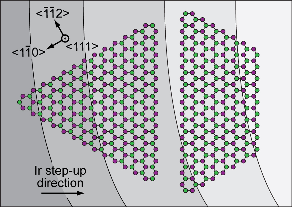
Atomically thin hBN islands of excellent crystal quality and size up to μm can be easily synthesized on the (111) surface of Ir via CVD process with borazine as a precursor. Two types of hBN islands have been observed: triangular and trapezoidal, which are rotated by 180° with respect to each other and which have ZZ edges. Both island types have the same atom species on all edges (presumably boron, based on the DFT calculations from Ref. Farwick zum Hagen et al. (2016)) except for the short base of the trapezoidal islands where an edge of opposite composition must exist. These structural results are illustrated in Fig. 6. Based on photoemission and spectroscopic data, we conclude that different shapes of the islands originate from different interactions with Ir. Moreover, Ir steps are crucial for the growth of hBN because they break the mirror symmetry of the 180°-rotated islands, which triggers different growth modes of hBN. This results in either triangular or trapezoidal islands, and the short base of the trapezoidal islands always forms in the step-up direction of the Ir surface. For synthesis temperatures lower than °C, hBN disintegration and dissolution of B in the Ir subsurface areas are greatly inhibited and hence such temperatures should be used in order to avoid formation of boron reconstructed regions. In these regions, boron atoms either fill large areas of Ir terraces (Bb regions) or form small irregular patches attached to hBN islands (Bw regions). This provides new possibilities for the production of other novel boron-based 2D materials, such as borophene. Overall, our results give new insights into CVD synthesis of hBN and can be used to steer future production of this important 2D material.
V Acknowledgments
Marko Kralj is acknowledged for critical reading of the manuscript and useful discussions. M.P. would like to thank the Alexander von Humboldt Foundation for financial support.
VI References
References
- Xu et al. (2013) M. Xu, T. Liang, M. Shi, and H. Chen, Chem. Rev. 113, 3766 (2013).
- Pakdel et al. (2014) A. Pakdel, Y. Bando, and D. Golberg, Chem. Soc. Rev. 43, 934 (2014).
- Cassabois et al. (2016) G. Cassabois, P. Valvin, and B. Gil, Nat. Photonics 10, 262 (2016).
- Dean et al. (2010) C. R. Dean, A. F. Young, I. Meric, C. Lee, L. Wang, S. Sorgenfrei, K. Watanabe, T. Taniguchi, P. Kim, K. L. Shepard, and J. Hone, Nat. Nanotechnol. 5, 722 (2010).
- Bresnehan et al. (2012) M. S. Bresnehan, M. J. Hollander, M. Wetherington, M. LaBella, K. A. Trumbull, R. Cavalero, D. W. Snyder, and J. A. Robinson, ACS Nano 6, 5234 (2012).
- Levendorf et al. (2012) M. P. Levendorf, C.-J. Kim, L. Brown, P. Y. Huang, R. W. Havener, D. A. Muller, and J. Park, Nature 488, 627 (2012).
- Lee et al. (2015) G.-H. Lee, X. Cui, Y. D. Kim, G. Arefe, X. Zhang, C.-h. Lee, F. Ye, K. Watanabe, T. Taniguchi, P. Kim, and J. Hone, ACS Nano 9, 7019 (2015).
- Watanabe et al. (2004) K. Watanabe, T. Taniguchi, and H. Kanda, Nat. Mater. 3, 404 (2004).
- Corso et al. (2004) M. Corso, W. Auwärter, M. Muntwiler, A. Tamai, T. Greber, and J. Osterwalder, Science 303, 217 (2004).
- Schulz et al. (2013) F. Schulz, R. Drost, S. K. Hämäläinen, and P. Liljeroth, ACS Nano 7, 11121 (2013).
- Auwärter et al. (1999) W. Auwärter, T. Kreutz, T. Greber, and J. Osterwalder, Surf. Sci. 429, 229 (1999).
- Morscher et al. (2006) M. Morscher, M. Corso, T. Greber, and J. Osterwalder, Surf. Sci. 600, 3280 (2006).
- Goriachko et al. (2007) A. Goriachko, Y. He, M. Knapp, H. Over, M. Corso, T. Brugger, S. Berner, J. Osterwalder, and T. Greber, Langmuir 23, 2928 (2007).
- Ćavar et al. (2008) E. Ćavar, R. Westerström, A. Mikkelsen, E. Lundgren, A. Vinogradov, M. L. Ng, A. Preobrajenski, A. Zakharov, and N. Mårtensson, Surf. Sci. 602, 1722 (2008).
- Dong et al. (2010) G. Dong, E. B. Fourré, F. C. Tabak, and J. W. M. Frenken, Phys. Rev. Lett. 104, 096102 (2010).
- Müller et al. (2010) F. Müller, S. Hüfner, H. Sachdev, R. Laskowski, P. Blaha, and K. Schwarz, Phys. Rev. B 82, 113406 (2010).
- Orlando et al. (2012) F. Orlando, R. Larciprete, P. Lacovig, I. Boscarato, A. Baraldi, and S. Lizzit, The Journal of Physical Chemistry C 116, 157 (2012).
- Joshi et al. (2012) S. Joshi, D. Ecija, R. Koitz, M. Iannuzzi, A. P. Seitsonen, J. Hutter, H. Sachdev, S. Vijayaraghavan, F. Bischoff, K. Seufert, J. V. Barth, and W. Auwärter, Nano Lett. 12, 5821 (2012).
- Wintterlin and Bocquet (2009) J. Wintterlin and M.-L. Bocquet, Surface Science 603, 1841 (2009).
- Celasco et al. (2017) E. Celasco, G. Carraro, M. Smerieri, L. Savio, M. Rocca, and L. Vattuone, The Journal of Chemical Physics 146, 104704 (2017).
- Preobrajenski et al. (2005) A. B. Preobrajenski, A. S. Vinogradov, and N. Mårtensson, Surf. Sci. 582, 21 (2005).
- Preobrajenski et al. (2007a) A. B. Preobrajenski, A. S. Vinogradov, M. L. Ng, E. Ćavar, R. Westerström, A. Mikkelsen, E. Lundgren, and N. Mårtensson, Phys. Rev. B 75, 245412 (2007a).
- Laskowski and Blaha (2010) R. Laskowski and P. Blaha, Phys. Rev. B 81, 075418 (2010).
- Preobrajenski et al. (2007b) A. B. Preobrajenski, M. A. Nesterov, M. L. Ng, A. S. Vinogradov, and N. Mårtensson, Chem. Phys. Lett. 446, 119 (2007b).
- Laskowski et al. (2008) R. Laskowski, P. Blaha, and K. Schwarz, Phys. Rev. B 78, 045409 (2008).
- Kralj et al. (2011) M. Kralj, I. Pletikosić, M. Petrović, P. Pervan, M. Milun, A. T. N’Diaye, C. Busse, T. Michely, J. Fujii, and I. Vobornik, Phys. Rev. B 84, 075427 (2011).
- Orlando et al. (2014) F. Orlando, P. Lacovig, L. Omiciuolo, N. G. Apostol, R. Larciprete, A. Baraldi, and S. Lizzit, ACS Nano 8, 12063 (2014).
- Farwick zum Hagen et al. (2016) F. H. Farwick zum Hagen, D. M. Zimmermann, C. C. Silva, C. Schlueter, N. Atodiresei, W. Jolie, A. J. Martínez-Galera, D. Dombrowski, U. A. Schröder, M. Will, P. Lazić, V. Caciuc, S. Blügel, T.-L. Lee, T. Michely, and C. Busse, ACS Nano 10, 11012 (2016).
- Usachov et al. (2012) D. Usachov, A. Fedorov, O. Vilkov, V. K. Adamchuk, L. V. Yashina, L. Bondarenko, A. A. Saranin, A. Grüneis, and D. V. Vyalikh, Phys. Rev. B 86, 155151 (2012).
- Mannix et al. (2015) A. J. Mannix, X.-F. Zhou, B. Kiraly, J. D. Wood, D. Alducin, B. D. Myers, X. Liu, B. L. Fisher, U. Santiago, J. R. Guest, M. J. Yacaman, A. Ponce, A. R. Oganov, M. C. Hersam, and N. P. Guisinger, Science 350, 1513 (2015).
- Zhang et al. (2015) Y. Zhang, X. Weng, H. Li, H. Li, M. Wei, J. Xiao, Z. Liu, M. Chen, Q. Fu, and X. Bao, Nano Lett. 15, 3616 (2015).
- Goriachko et al. (2008) A. Goriachko, A. A. Zakharov, and H. Over, The Journal of Physical Chemistry C 112, 10423 (2008).
- Sutter et al. (2011) P. Sutter, J. Lahiri, P. Albrecht, and E. Sutter, ACS Nano 5, 7303 (2011).
- Orofeo et al. (2013) C. M. Orofeo, S. Suzuki, H. Kageshima, and H. Hibino, Nano Res. 6, 335 (2013).
- Kim et al. (2012) K. K. Kim, A. Hsu, X. Jia, S. M. Kim, Y. Shi, M. Hofmann, D. Nezich, J. F. Rodriguez-Nieva, M. Dresselhaus, T. Palacios, and J. Kong, Nano Lett. 12, 161 (2012).
- N’Diaye et al. (2009) A. T. N’Diaye, R. van Gastel, A. J. Martínez-Galera, J. Coraux, H. Hattab, D. Wall, F.-J. Meyer zu Heringdorf, M. Horn-von Hoegen, J. M. Gómez-Rodríguez, B. Poelsema, C. Busse, and T. Michely, New J. Phys. 11, 113056 (2009).
- Petrović et al. (2015) M. Petrović, J. T. Sadowski, A. Šiber, and M. Kralj, Carbon 94, 856 (2015).
- Lee et al. (2008) C. Lee, X. Wei, J. W. Kysar, and J. Hone, Science 321, 385 (2008).
- Song et al. (2010) L. Song, L. Ci, H. Lu, P. B. Sorokin, C. Jin, J. Ni, A. G. Kvashnin, D. G. Kvashnin, J. Lou, B. I. Yakobson, and P. M. Ajayan, Nano Lett. 10, 3209 (2010).
- Arblaster (2010) J. W. Arblaster, Platin. Met. Rev. 54, 93 (2010).
- Paszkowicz et al. (2002) W. Paszkowicz, J. Pelka, M. Knapp, T. Szyszko, and S. Podsiadlo, Appl. Phys. A: Mater. Sci. Process. 75, 431 (2002).
- Schulz et al. (2014) F. Schulz, R. Drost, S. K. Hämäläinen, T. Demonchaux, A. P. Seitsonen, and P. Liljeroth, Phys. Rev. B 89, 235429 (2014).
- Cornish and Avery (1990) J. C. Cornish and N. R. Avery, Surf. Sci. 235, 209 (1990).
- Zeiringer et al. (2015) I. Zeiringer, X. Cheng, X.-Q. Chen, E. Bauer, G. Giester, and P. F. Rogl, Science China Materials 58, 649 (2015).
- Sutter and Sutter (2014) P. Sutter and E. Sutter, APL Materials 2, 092502 (2014).
- Zhang et al. (2016) Z. Zhang, Y. Liu, Y. Yang, and B. I. Yakobson, Nano Lett. 16, 1398 (2016).
- Liu et al. (2014) M. Liu, Y. Li, P. Chen, J. Sun, D. Ma, Q. Li, T. Gao, Y. Gao, Z. Cheng, X. Qiu, Y. Fang, Y. Zhang, and Z. Liu, Nano Lett. 14, 6342 (2014).
- Auwärter et al. (2003) W. Auwärter, M. Muntwiler, J. Osterwalder, and T. Greber, Surf. Sci. 545, L735 (2003).
- Lu et al. (2013) J. Lu, P. S. E. Yeo, Y. Zheng, H. Xu, C. K. Gan, M. B. Sullivan, A. Castro Neto, and K. P. Loh, J. Am. Chem. Soc. 135, 2368 (2013).
- Grad et al. (2003) G. B. Grad, P. Blaha, K. Schwarz, W. Auwärter, and T. Greber, Phys. Rev. B 68, 085404 (2003).
- Camilli et al. (2014) L. Camilli, E. Sutter, and P. Sutter, 2D Materials 1, 025003 (2014).
- N’Diaye et al. (2008) A. T. N’Diaye, J. Coraux, T. N. Plasa, C. Busse, and T. Michely, New J. Phys. 10, 043033 (2008).
- Coraux et al. (2008) J. Coraux, A. T. N’Diaye, C. Busse, and T. Michely, Nano Lett. 8, 565 (2008).
- Hattab et al. (2011) H. Hattab, A. T. N’Diaye, D. Wall, G. Jnawali, J. Coraux, C. Busse, R. van Gastel, B. Poelsema, T. Michely, F.-J. Meyer zu Heringdorf, and M. Horn-von Hoegen, Appl. Phys. Lett. 98, 141903 (2011).
- Babout et al. (1980) M. Babout, C. Guittard, M. Guivarch, R. Pantel, and M. Bujor, J. Phys. D: Appl. Phys. 13, 1161 (1980).
- Strayer et al. (1973) R. Strayer, W. Mackie, and L. Swanson, Surf. Sci. 34, 225 (1973).
- Starodub et al. (2011) E. Starodub, A. Bostwick, L. Moreschini, S. Nie, F. E. Gabaly, K. F. McCarty, and E. Rotenberg, Phys. Rev. B 83, 125428 (2011).
- Niesner et al. (2012) D. Niesner, T. Fauster, J. I. Dadap, N. Zaki, K. R. Knox, P.-C. Yeh, R. Bhandari, R. M. Osgood, M. Petrović, and M. Kralj, Phys. Rev. B 85, 081402 (2012).
- Šrut Rakić et al. (2016) I. Šrut Rakić, M. Kralj, W. Jolie, P. Lazić, W. Sun, J. Avila, M.-C. Asensio, F. Craes, V. Mikšić Trontl, C. Busse, and P. Pervan, Carbon 110, 267 (2016).