Topological electronic properties of silicon
Abstract
The central role that materials play in human history is exemplified by the three-age division of prehistory into the stone, bronze, and iron ages. References to our present time as the information age or silicon age epitomizes the important role that this semiconducting material came to play in the development of computers and devices that permeate our daily lives. Here we show that the electronic states in silicon have nontrivial topological structures that are captured by a network of Berry flux lines that link at points of high symmetry in the Brillouin zone. This complex network has ice-nodal points where fluxes satisfy ice rules, making silicon a “nodal-chain insulator”. Fixing the longitudinal momentum parallel to such flux lines yields a two-dimensional Dirac Hamiltonian for the transverse degrees of freedom. This complex Berry-flux network implies a topologically stable two-fold degeneracy along the X-W direction in all of silicon bands, a fact that is supported by crystal symmetry arguments as well as direct inspection of the vast literature on silicon band structures. Similarly to nodal-chain semimetals, we find drumhead-like states in the regions that are delimited by the projections of the bulk Berry flux network on the surface Brillouin zone.
I Introduction
The experimental discovery of the integer quantum Hall effect [1], where the Hall resistance is quantized to the extraordinary precision of one part in a billion, led to the new standard of resistance for the international system of units. A degree of precision such as this has its roots in a fruitful confluence of physics and mathematics, which ties the Hall resistance to a topological quantity. In the case of the integer Hall effect, this quantity is the first Chern number associated to each filled Landau level [2]. The integer Hall effect was the first example of a system with topological electronic properties; the number of systems in which topology plays a prominent role has grown explosively in the recent past, fueled by the discovery of a new class of topological band insulators occurring in semiconductors with strong spin-orbit coupling, in which gapless surface states exist [3, 4, 5, 6, 7, 8, 9, 10, 11, 12, 13, 14, 15, 16] (For reviews, see Refs. 17, 18.) After the discovery of topological insulators, many examples of topological semimetals were identified, such as Weyl metals [19, 20, 21, 22, 23, 24, 25] and systems with Weyl nodal lines [19, 26], and nodal chains [27].
Spin-orbit interactions play a prominent role in the topological insulators and Weyl systems, but spin-orbit coupling is not central to the understanding of the basic electronic properties of silicon. Indeed, in the standard classification of topological insulators, silicon is not classified [28] as one with protected Dirac surface states. Therefore, silicon thus far has sat on the sidelines. Here we show that the sublattice structure of crystals such as silicon is responsible for a network of Berry flux lines in the Brillouin zone that link at points of high symmetry in momentum space. This Berry flux network is topologically stable, obeys ice rules (two in, two out) at the X points, and is responsible for topological protection of degeneracies along the X-W direction. The nontrivial topological structure of the Berry flux network in silicon shares the same physical origin as the Berry flux in graphene: the fact that there are two atoms in the unit cell gives rise to a spinor structure with associated Berry phases. The existence of the Berry flux network opens a novel “topological knob” to manipulate electrons in silicon, especially in light of progress made in the past decade from studying the effects of Berry phases in the electronic properties in graphene.
II Berry flux network
We uncover the Berry flux network in two steps. First we identify the spinor structure and the Berry fluxes within a general tight-binding approximation (valid for an arbitrary number of orbitals). Second we argue based on topological and symmetry arguments that the Berry flux network is robust and remains beyond the tight-binding description of silicon.
A tight-binding Hamiltonian for a system on a bipartite lattice comprised of sublattices and can be represented as
| (1) |
where the blocks and contain hoppings between sites in the same sublattice, and the blocks and contain hoppings between sites is different sublattices. The size of these blocks depend on the number of orbitals included in the tight-binding model. For example, in graphene the blocks are if one considers only the -orbital, and in silicon the blocks are if one takes account of only the orbitals (or in the model [29], with the inclusion of the orbital). The diagonal blocks are periodic in -space: and , where () is a reciprocal lattice basis vector ( for graphene, for silicon). The matrix elements of the off-diagonal blocks are written as
| (2) |
where the vectors connect the atoms from to , and the contain the overlap of the orbitals and separated by . Because the vectors are not Bravais lattice vectors, is generically not a multiple of , and therefore the off-diagonal blocks and are not periodic in -space. An attempt to gauge out these non-periodicities comes with the price of adding singularities (branch cuts) to the phase of the wave function in momentum space.
In graphene the vectors , , point to the vertices of a triangle, while in silicon the , , point to the vertices of a tetrahedron. In these lattices (see Supplementary Online Information), it follows that , where , with and for the graphene and silicon lattices, respectively. The Hamiltonian is not periodic in -space; however, it is periodic up to a unitary transformation that rotates the amplitudes on the two sublattices by opposite phases:
| (3) |
with
| (4) |
and a Pauli matrix acting on the sublattice grading. It follows from Eq. (3) that the eigenenergies , as expected. However, the spinor structure and the lack of periodicity of the matrix Hamiltonian (not just its eigenvalues) is what leads to the Berry -vortices at the points in graphene, and the Berry -flux network that we uncover in this work. (In the Supplementary Online Information we illustrate how the generic framework above recovers the familiar results in graphene as a warm up for the calculations in silicon.)
Consider the walk in -space that visits, in order, the points and back to . This walk passes through 4 of the 6 edges of the tetrahedron formed by the four points in -space, closing a loop. We choose the initial point not to be one of high symmetry, to avoid that the edges pass through band crossings, thus avoiding degeneracies along the walk. For example, one may choose to start close to but not at the point, say at , with infinitesimal . At the end of the walk, the Hamiltonian returns to , but the eigenvector is rotated by the sequence of unitary operations
| (5) |
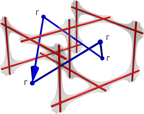
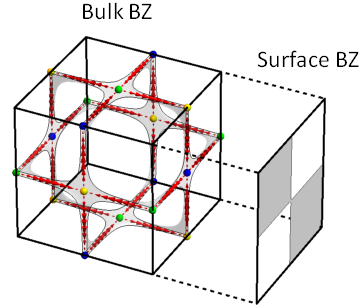
which amounts to a rotation by [30]. This geometric phase implies the existence of -flux lines in -space, which pierce the loop we described above. An example of a -flux network that threads the 4-edged loop in -space is shown in Fig. 1, which, as we show below, corresponds to the cases of the lowest conduction and valence bands in silicon.
These singular flux lines are stable, and cannot be removed by small deformations. Silicon is inversion symmetric, which implies that the Berry curvature ; in the absence of time-reversal breaking perturbations, . These two symmetries, together, imply that the Berry curvature vanishes everywhere with the possible exception of singular lines carrying flux multiple of , like those we identified above. These two symmetries thus ensure that the -flux cannot spread over a finite region, and thus remains singular and contained within a network of flux lines circulating around the Brillouin zone. The number of orbitals in the description of the system does not alter our conclusions based on the topological constraints imposed by Eq. (5).
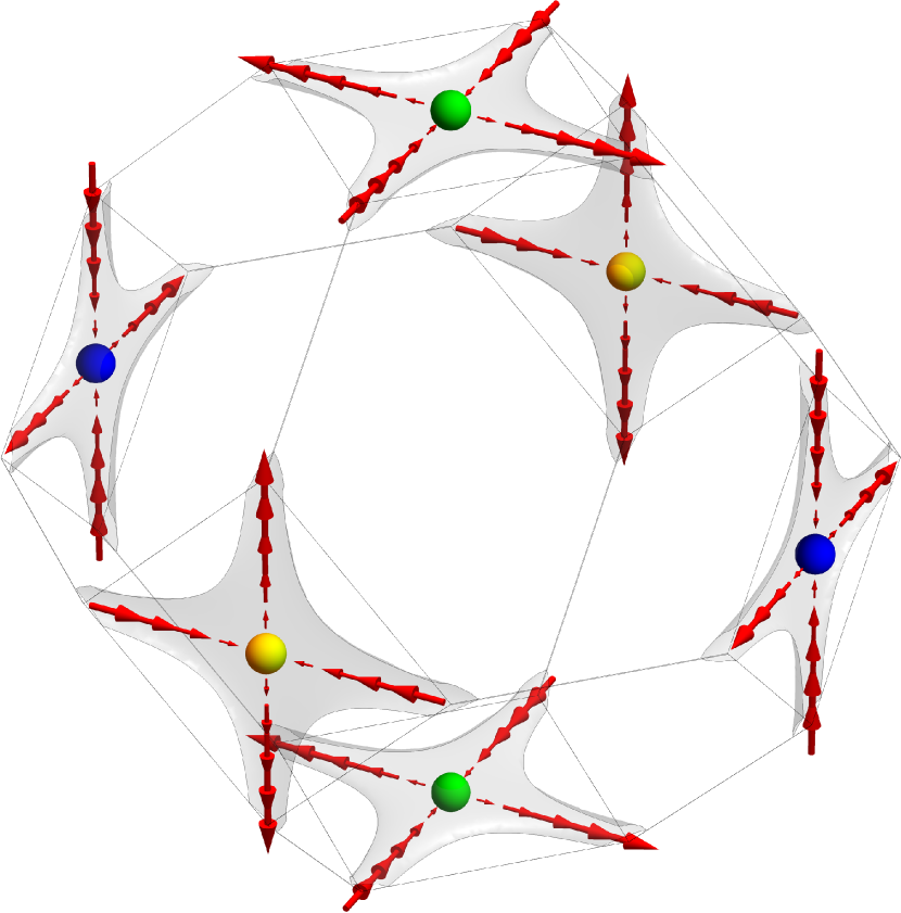
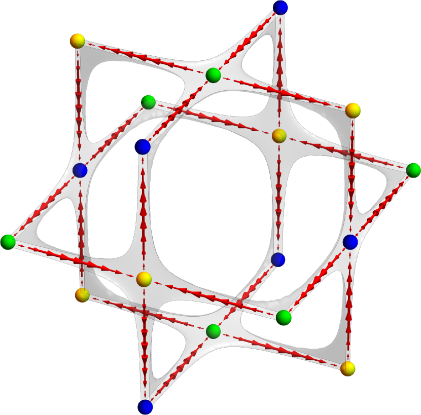
To visualize the network of fluxes in silicon, we consider explicitly the 5-orbital nearest-neighbor tight-binding model [29]. This model captures essential features of silicon’s band structure; in particular, it reproduces the conduction band minimum along the line connecting the and X points in the Brillouin zone. In this approximation, sites within the same sublattice are not connected, so that diagonal blocks simply contain the on-site potential energies , while the inter-sublattice hoppings contain the non-trivial momentum dependence:
| (6) |
where momentum functions
| (7) |
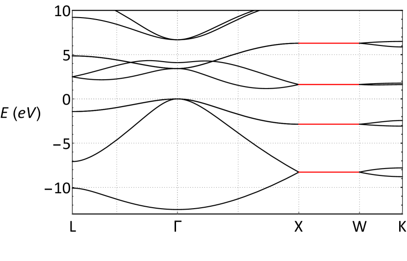
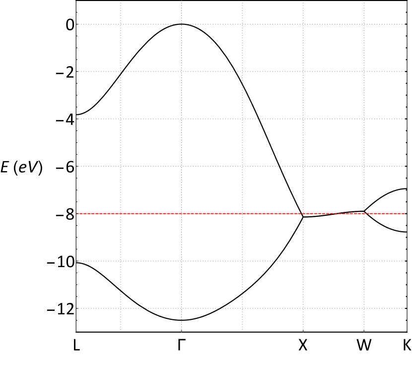
and , , , and , with Å. The interaction parameters in the Hamiltonian are (in eV) [29]. The resulting band structure is shown in Fig. 3.
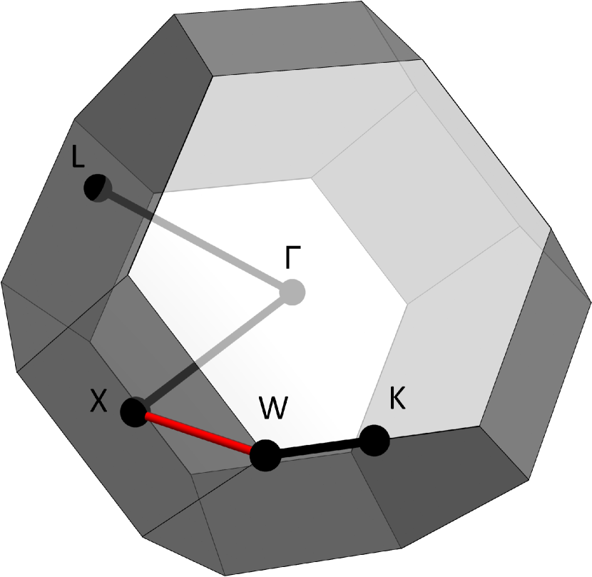
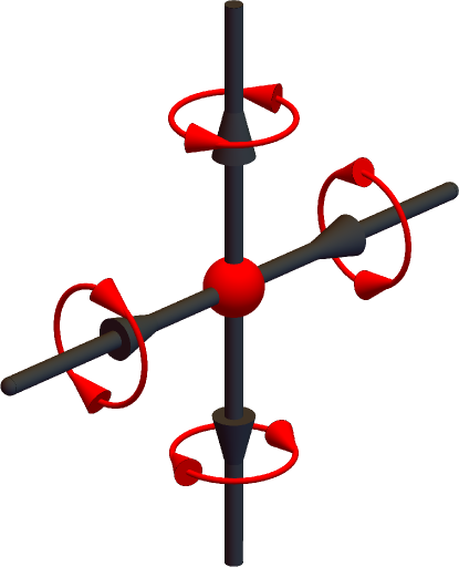
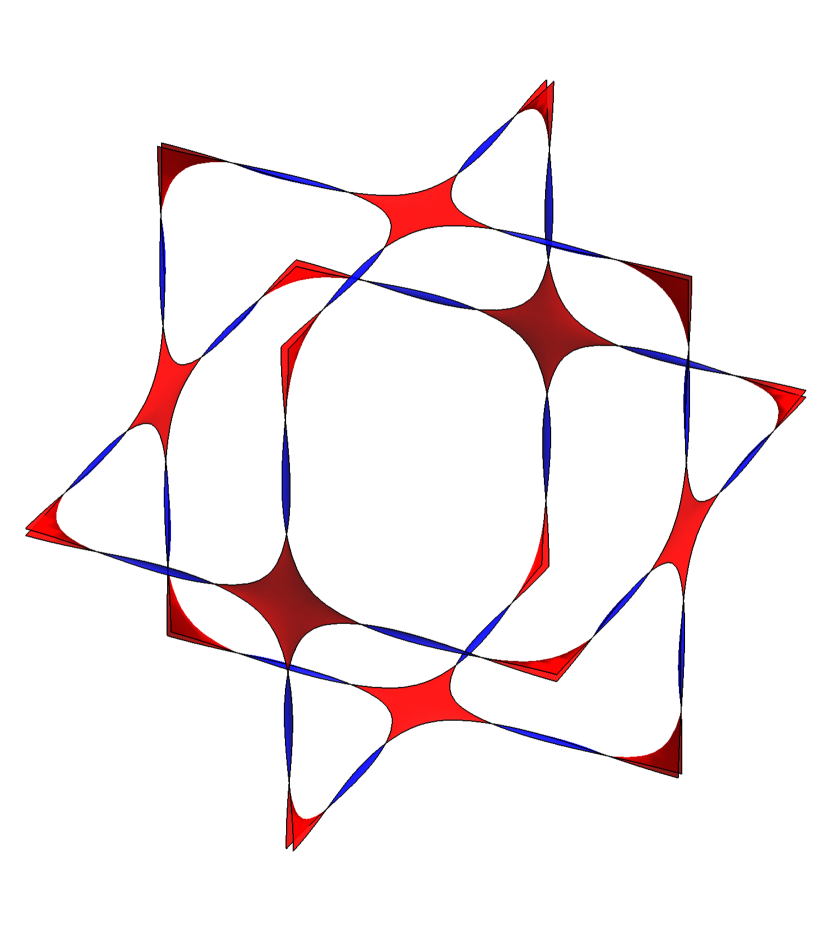
This spectrum has an intricate set of lines along which the spectrum is twofold degenerate, in particular along the Z line connecting the X and W points, which is consistent with the crystal symmetry of silicon [31]. We argue that these degeneracies, associated with the Berry flux identified above, correspond to Dirac lines: fixing the longitudinal momentum along the line yields a two-dimensional Dirac Hamiltonian for the transverse degrees of freedom. While the dispersionless nature of these lines along their longitudinal direction is an artifact of the nearest-neighbor tight-binding approximation, the two-fold degeneracy and the Berry -flux that travels along these lines are robust. We remark that distorting the hoppings would not remove these lines of degeneracy because the -fluxes are topologically stable; hence topology ensures that there should be lines of degeneracy in silicon even if rotational symmetry is broken but sublattice symmetry is not. (An analogous reasoning holds in graphene, where the nodes are stable even if the hopping matrix elements to the three neighbors are close but unequal.) We find that the lowest conduction and valence bands exhibit the simplest pattern of these Berry flux lines, which reduce to a cage-like net of Dirac lines connecting inequivalent X points (going along the Z line through both X and W points), as is shown on the Fig. 2. The Dirac lines meet at the X point, forming an ice-nodal point (Fig. 4).
III Effective Hamiltonian near the X point of the lowest conduction band
The effective two-band Hamiltonian in the vicinity of the ice-nodal point of the first conduction band is obtained by expanding , yielding (see Supplementary Online Information for details)
| (8) |
where , , , and are Pauli matrices. (Energies are measured in eV and momentum in units of .) This expression explicitly shows the ice-nodal nature of the X point. For example, in the vicinity of the points the Hamiltonian takes the form
| (9) |
where and are electron velocities at the points. This Hamiltonian structure indicates two Dirac lines with opposite chiralities approaching the X point along the -axis from opposite directions. Similarly, there are two more such lines along the -axis (see Fig. 4).
It turns out that all crucial topological properties of the conduction band can be studied within a simple toy model, with a single orbital per site and nearest-neighbor tight-binding Hamiltonian
| (10) |
Hopping matrix elements to farther neighbors can be included, especially between the sites of the same sublattice, to reproduce features of silicon’s band structure, such as a conduction band minimum along the line. Yet, the topological features are captured by the off-diagonal terms alone: the Hamiltonian is degenerate along the manifold, yielding essentially the same cage-like net of Dirac lines connecting at X points, just as in the full model for silicon.
The real and imaginary parts of are
| (11) |
from which we identify
| (12) |
as the set of nodal lines, crossing at the three ice-nodal X points,
| (13) |
Expanding around one of the ice-nodal points, , we obtain
| (14) |
reproducing the same structure of the X-point effective Hamiltonian derived using the model:
| (15) |
We note that perturbing this toy model Hamiltonian with a term gaps out the Dirac lines (it breaks sublattice symmetry), while a perturbation separates the Dirac lines in different ways depending on the sign of the term, indicating the critical character of the ice-nodal point.
Finally, we gather all results above on the ice-nodal points and combine them with other information inferred from results on the band structure of silicon that is obtained from methods other than tight-binding. We condense this combined information into an effective Hamiltonian near the nodal point:
| (16) |
where and coincide with the masses from the standard low-energy description of the conduction band (with the electron mass); the velocity is estimated from the location of the conduction band minimum; and follows from the dispersion along the X-U direction. This effective Hamiltonian, we claim, captures the topological properties and hence gives a more accurate description of the low energy states in silicon’s conduction band than simply expanding the dispersion to quadratic order near the band minimum. That the minimum occurs close to the X point is captured by the interplay between the Dirac dispersion along the -direction and the parabolic term, which places the minimum close to the X point (notice that the energy difference between the minimum and the X point is only 0.08eV [32]).
IV Surface states and bulk-boundary correspondence
Probably the most important theoretical insight in the field of topological insulators is the fact that non-trivial bulk topology leads to the existence of robust surface states. Recently this idea was extended to topological semimetals, where the Fermi surface consists of a nodal loop. In such materials surface states exist only in parts of the surface Brillouin zone that are determined by projecting the nodal loop from the bulk Brillouin zone onto the surface Brillouin zone. Here we argue that the same bulk-boundary correspondence applies to silicon and the existence of the Berry flux “wire frame” leads to the existence of non-trivial topological drumhead surface states.
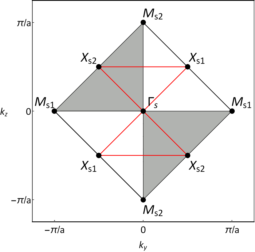
The two-band toy model Hamiltonian (10) is of an archetypal semimetallic and the manifold defines a nodal loop. Moreover, this Hamiltonian describes a nodal chain semimetal, a topologically critical system with crossing nodal lines yielding ice-nodal X points[27, 33]. According to the intuition from semimetallic systems[34, 35, 36, 37], the projection of the bulk wire frame onto the surface Brillouin zone breaks it into segments. These segments can be colored with two colors, for example red and blue, in such way that adjacent parts are always of the opposite color. Surface drumhead states then exist in all segments colored either in blue or in red, depending whether the crystal surface is terminated at A or B sublattice. In the case of silicon that we consider, the projection of the wire frame breaks down surface Brillouin zone into quadrants. Surface states exist either in first and third or second and fourth quadrants, see Fig. 5.
In the nearest neighbor toy model, chiral symmetry protects the dispersionless nature of the wire frame and the Fermi Surface at this energy coincides with the wire frame. The same happens at the touching of the two lowest valence bands in the model, see Fig. 3. In real silicon, however, lines possess nontrivial dispersion. Hopping matrix elements to farther neighbors can be included in order to break sublattice symmetry and reproduce this feature:
| (17) |
where
| (18) | ||||
| (19) |
We allow for both next-nearest-neighbor () and next-next-nearest-neighbor () hopping. It turns out that hopping alone is not sufficient to destroy the flatness of dispersion along X-W lines. We fit parameters of the toy model to reproduce point energies in the lowest valence band of real silicon. The resulting band structure and Fermi surface in the vicinity of the X point are shown in Fig. 6.
V Silicon quantum well
The clean and straightforward connection between bulk topology and surface states relies on the sublattice symmetry, which, unfortunately, is destroyed even within the model. While model has matrix elements only between A and B sublattices, only two of the ten states are involved in the formation of each wire frame. When the full Hamiltonian is projected on the relevant two dimensional subspace for each wire frame, longer range hopping elements are induced via transitions to the states that were projected out. For example, if we focus on the lowest energy wire frame that is formed by the first two bands, next-nearest neighbor element between an A site at the i-th and (i+1)-th cells is formed as
| (20) |
Despite this unfortunate fact, the bulk-boundary correspondence and surface states in the toy model are of topological nature. Hence, we expect that breaking respective symmetries retains qualitatively bulk-boundary correspondence and surface states for reasonably large perturbations of the toy model.
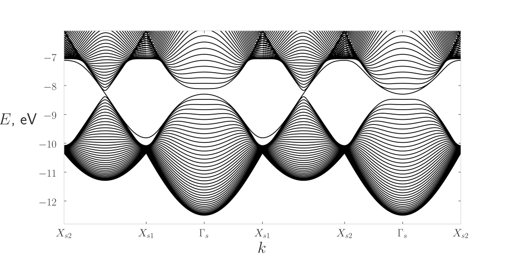
To explore drumhead states within the model, we perform a numerical calculation of the electron dispersion in a silicon slab. We consider a slab of the material with [100] surface and the thickness approximately 20 nm (40 unit cells). The sample is infinite in the directions parallel to the surface, for which we perform the Fourier transformation, retaining only the spatial dimension perpendicular to the surface, so that the electron wavefunction can be factorized as
| (21) |
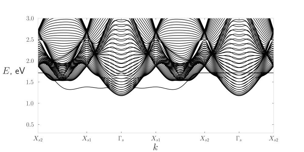
where is the position of the -th unit cell (), labels A/B sublattices and enumerates each of the five orbitals. We find all eigenvalues of the Hamiltonian for each value of the momentum parallel to the surface and repeat this procedure along the path within the surface Brillouin zone. The result is shown on the Fig. 7. While the exact nature of the bulk-boundary correspondence does not survive in the five band model, the qualitative connection remains clear.
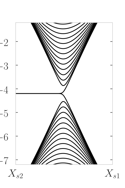
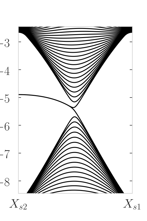
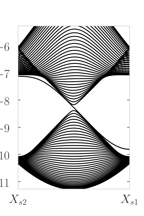
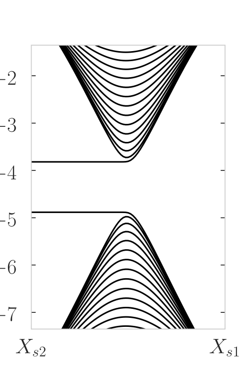
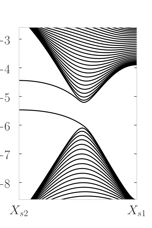
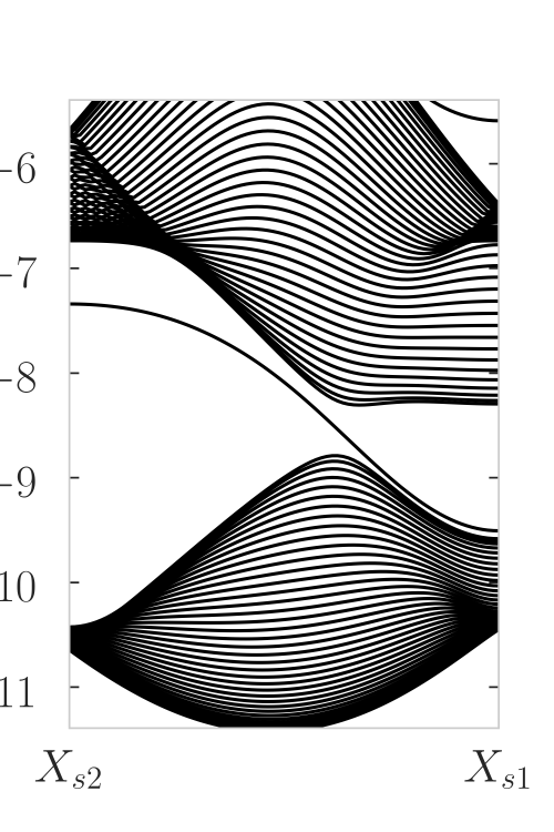
As we have argued in the previous section, the energy dispersion of silicon in the vicinity of the touching of the lowest valence bands is fairly close to that of the toy model. Largely, this is the case due to other bands being well separated in energy from the first two valence bands. To further clarify the connection between the surface states and the bulk topology, we consider the following modification of the model. We slowly tune interband hopping parameters from 0 to ,
| (22) |
keeping other parameters intact. At we have five exactly solvable copies of the toy model and for each of them we know that the drumhead states exist and they are of topological nature. This way, by slowly tuning from to , we can track the evolution of the surface state arising from the lowest energy wire frame.
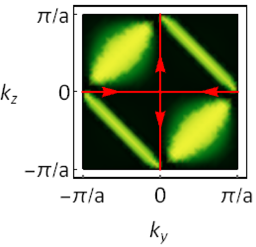
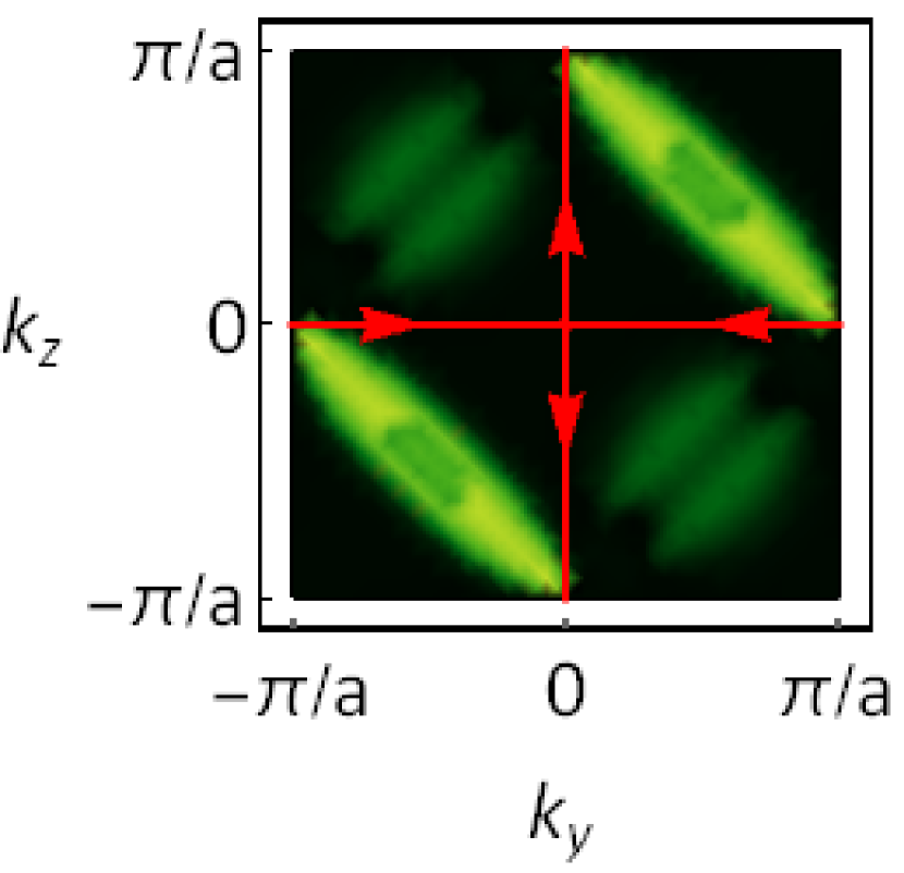
In Fig. 8 we zoom into the region between points and , to show a striking robustness of the drumhead state in the full model. On the top panels, we show the evolution of the spectrum for , and 1.0, and on the bottom panels we show the spectrum resulting from further addition of a term that breaks inversion symmetry and opens a gap. Notice that the drumhead states acquire a dispersion as is turned on, and that the corresponding bandwidth is large. Thus, if one opens a gap that is smaller than that bandwidth (as in the bottom panels), a stable drumhead state remains at the surface, crossing the bulk gap. We remark that the scale of the bandwidth is rather large in the model, of the order of several . In other words, breaking of the chiral symmetry protects the drumhead state against other perturbations that weakly break any other symmetry.
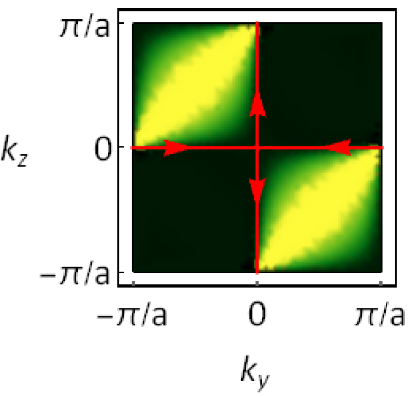

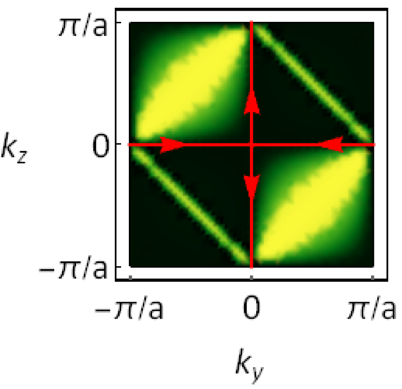

In addition to tracking the -dependence of the energy spectrum, for each value of we also calculate the inverse participation ratio defined as
| (23) |
For localized states the ipr is inversely proportional to the localization length , while for bulk states it vanishes as , where is the size of the system. The resulting inverse participation ratios are shown in the Fig. 9. Aside from the emergence of new surface states as we tune , the topological nature this surface state is unambiguous.
VI Conclusions and Outlook
In this work we identified a network of Berry flux lines in reciprocal space, for silicon. We first constructed a rather general argument, based solely on the existence of two sublattices, to argue that there must be flux lines independently of how many bands there are. The flux lines are tied to the spinor structure due to the two sublattices, and the flux cannot spread out because of time-reversal and inversion symmetry. The situation is analogous to what happens in graphene, where the Dirac points carry flux and cannot be removed perturbatively.
We then identified these lines in a tight-binding model containing 5-orbitals per sublattice (a matrix Hamiltonian). We showed explicitly that the flux lines appear, and identified the point as a location where flux lines meet. The electronic dispersion near the point can be described in terms of the Dirac lines analyzed in this paper.
Flux lines inside the bulk Brillouin zone imply the existence of drumhead surface states, which are confined within the projection of the flux lines onto the surface Brillouin zone. We discussed how the breaking of sublattice symmetry makes the identification of the drumhead states less obvious, but that nevertheless the qualitative connection between bulk-boundary remains.
There are two sets of questions that our work suggests:
-
•
Can one observe all or some of these features experimentally?
-
•
Can the knowledge that these topological features exist in silicon lead to novel electronics in this “old” material?
Regarding the first question, one of the possible tools to probe these flux lines and the dispersion of wire frames is angle resolved photoemission spectroscopy (ARPES). Since the features we identified are present in all bands of silicon, one can study them in the valence bands, which are accessible in ARPES. If high energy photons are used, not only can one probe electronic states deep inside the valence bands but also use the high penetration depth (here the -direction) of those photons to map constant energy surfaces as function of and for different . Such techniques are used in Ref. 38, for example. These types of scans would be able to identify the wire frames, providing evidence for the lines of nodes where the flux runs through.
As for addressing the second question, one must find ways to pull the physics of these nodal lines or surface states to the Fermi level. While the Fermi level lies in the gap for intrinsic silicon, one can reach the regime where the Fermi level crosses the conduction band in inversion layers in doped silicon field effect transistors (FETs).
Another possibility is to use undoped silicon, and pull down the surface states by electric fields. States that are already localized at the boundary are more sensitive to potentials caused by an electric field (a linear potential has its largest and smallest values at the boundary). Intrinsic silicon cannot screen the electric field. Once the surface states are pulled to the Fermi level, there should be metallic boundary states. The absence of disorder should lead to high mobilities at these surfaces. While the mechanism described above does not require that the surface states be drumhead ones, we already observe from Fig. 7 that the lowest surface band at positive energies is of the drumhead type.
The findings presented in this work reveal novel topological electronic features in the band structure of silicon, one of the best known and most studied materials. That these features had been missed does not signal an accident, but rather suggests that there are a number of topological properties occuring in many, if not most, other materials. The topological features of silicon that we expose provide new impetus to revisit the physics of bulk silicon and two-dimensional electron gases in silicon FETs, particularly in light of what is now known from recent studies of both graphene and topological insulators.
Acknowledgements.
We thank Michael El-Batanouny, Shyam Erramilli, Thomas Iadecola, Christopher Mudry, Andrei Ruckenstein, and Alex Sushkov for insightful discussions. We acknowledge financial support from the U.S. Dept. of Energy Grant DE-FG02-06ER46316 (C.C.).References
- [1] K. v. Klitzing, G. Dorda, and M. Pepper. New method for high-accuracy determination of the fine-structure constant based on quantized Hall resistance. Phys. Rev. Lett., 45:494–497, Aug 1980.
- [2] D. J. Thouless, M. Kohmoto, M. P. Nightingale, and M. den Nijs. Quantized Hall conductance in a two-dimensional periodic potential. Phys. Rev. Lett., 49:405–408, Aug 1982.
- [3] C. L. Kane and E. J. Mele. Quantum spin Hall effect in graphene. Phys. Rev. Lett., 95:226801, Nov 2005.
- [4] C. L. Kane and E. J. Mele. topological order and the quantum spin Hall effect. Phys. Rev. Lett., 95:146802, Sep 2005.
- [5] Liang Fu and C. L. Kane. Time reversal polarization and a adiabatic spin pump. Phys. Rev. B, 74:195312, Nov 2006.
- [6] B. Andrei Bernevig and Shou-Cheng Zhang. Quantum spin Hall effect. Phys. Rev. Lett., 96:106802, Mar 2006.
- [7] B. Andrei Bernevig, Taylor L. Hughes, and Shou-Cheng Zhang. Quantum spin Hall effect and topological phase transition in HgTe quantum wells. Science, 314(5806):1757–1761, 2006.
- [8] Markus König, Steffen Wiedmann, Christoph Brüne, Andreas Roth, Hartmut Buhmann, Laurens W. Molenkamp, Xiao-Liang Qi, and Shou-Cheng Zhang. Quantum spin Hall insulator state in HgTe quantum wells. Science, 318(5851):766–770, 2007.
- [9] Liang Fu, C. L. Kane, and E. J. Mele. Topological insulators in three dimensions. Phys. Rev. Lett., 98:106803, Mar 2007.
- [10] J. E. Moore and L. Balents. Topological invariants of time-reversal-invariant band structures. Phys. Rev. B, 75:121306, Mar 2007.
- [11] Rahul Roy. classification of quantum spin Hall systems: An approach using time-reversal invariance. Phys. Rev. B, 79:195321, May 2009.
- [12] Rahul Roy. Topological phases and the quantum spin Hall effect in three dimensions. Phys. Rev. B, 79:195322, May 2009.
- [13] D. Hsieh, D. Qian, L. Wray, Y. Xia, Y. S. Hor, R. J. Cava, and M. Z. Hasan. A topological Dirac insulator in a quantum spin Hall phase. Nature, 452(7190):970–974, Apr 2008.
- [14] D. Hsieh, Y. Xia, L. Wray, D. Qian, A. Pal, J. H. Dil, J. Osterwalder, F. Meier, G. Bihlmayer, C. L. Kane, Y. S. Hor, R. J. Cava, and M. Z. Hasan. Observation of unconventional quantum spin textures in topological insulators. Science, 323(5916):919–922, 2009.
- [15] D. Hsieh, Y. Xia, D. Qian, L. Wray, J. H. Dil, F. Meier, J. Osterwalder, L. Patthey, J. G. Checkelsky, N. P. Ong, A. V. Fedorov, H. Lin, D. Bansil, A. eand Grauer, Y. S. Hor, R. J. Cava, and M. Z. Hasan. A tunable topological insulator in the spin helical Dirac transport regime. Nature, 460(7259):1101–1105, Aug 2009.
- [16] Y. L. Chen, J. G. Analytis, J.-H. Chu, Z. K. Liu, S.-K. Mo, X. L. Qi, H. J. Zhang, D. H. Lu, X. Dai, Z. Fang, S. C. Zhang, I. R. Fisher, Z. Hussain, and Z.-X. Shen. Experimental realization of a three-dimensional topological insulator, Bi2Te3. Science, 325(5937):178–181, 2009.
- [17] M. Z. Hasan and C. L. Kane. Colloquium: Topological insulators. Rev. Mod. Phys., 82:3045–3067, Nov 2010.
- [18] Xiao-Liang Qi and Shou-Cheng Zhang. Topological insulators and superconductors. Rev. Mod. Phys., 83:1057–1110, Oct 2011.
- [19] A. A. Burkov, M. D. Hook, and Leon Balents. Topological nodal semimetals. Phys. Rev. B, 84:235126, Dec 2011.
- [20] A. A. Burkov and Leon Balents. Weyl semimetal in a topological insulator multilayer. Phys. Rev. Lett., 107:127205, Sep 2011.
- [21] Xiangang Wan, Ari M. Turner, Ashvin Vishwanath, and Sergey Y. Savrasov. Topological semimetal and Fermi-arc surface states in the electronic structure of pyrochlore iridates. Phys. Rev. B, 83:205101, May 2011.
- [22] Madhab Neupane, Su-Yang Xu, Raman Sankar, Nasser Alidoust, Guang Bian, Chang Liu, Ilya Belopolski, Tay-Rong Chang, Horng-Tay Jeng, Hsin Lin, Arun Bansil, Fangcheng Chou, and M. Zahid Hasan. Observation of a three-dimensional topological Dirac semimetal phase in high-mobility Cd3As2. Nature Communications, 5:3786 EP –, May 2014. Article.
- [23] Z. K. Liu, B. Zhou, Y. Zhang, Z. J. Wang, H. M. Weng, D. Prabhakaran, S.-K. Mo, Z. X. Shen, Z. Fang, X. Dai, Z. Hussain, and Y. L. Chen. Discovery of a three-dimensional topological Dirac semimetal, Na3Bi. Science, 343(6173):864–867, 2014.
- [24] Shin-Ming Huang, Su-Yang Xu, Ilya Belopolski, Chi-Cheng Lee, Guoqing Chang, BaoKai Wang, Nasser Alidoust, Guang Bian, Madhab Neupane, Chenglong Zhang, Shuang Jia, Arun Bansil, Hsin Lin, and M. Zahid Hasan. A Weyl Fermion semimetal with surface Fermi arcs in the transition metal monopnictide TaAs class. Nature Communications, 6:7373 EP –, Jun 2015. Article.
- [25] B. Q. Lv, H. M. Weng, B. B. Fu, X. P. Wang, H. Miao, J. Ma, P. Richard, X. C. Huang, L. X. Zhao, G. F. Chen, Z. Fang, X. Dai, T. Qian, and H. Ding. Experimental discovery of Weyl semimetal TaAs. Phys. Rev. X, 5:031013, Jul 2015.
- [26] Rui Yu, Hongming Weng, Zhong Fang, Xi Dai, and Xiao Hu. Topological node-line semimetal and Dirac semimetal state in antiperovskite Cu3PdN. Phys. Rev. Lett., 115:036807, Jul 2015.
- [27] Tomáš Bzdušek, QuanSheng Wu, Andreas Ruegg, Manfred Sigrist, and Alexey A. Soluyanov. Nodal-chain metals. Nature, 538(7623):75–78, OCT 6 2016.
- [28] Andreas P. Schnyder, Shinsei Ryu, Akira Furusaki, and Andreas W. W. Ludwig. Classification of topological insulators and superconductors in three spatial dimensions. Phys. Rev. B, 78:195125, Nov 2008.
- [29] P. Vogl, Harold P. Hjalmarson, and John D. Dow. A semi-empirical tight-binding theory of the electronic structure of semiconductors. Journal of Physics and Chemistry of Solids, 44(5):365 – 378, 1983.
- [30] The Berry phase can be read directly from the product of unitary matrices because of our choice of gauge. Having the phases (for in graphene and in silicon) ensures that , and the overlap between spinors along the legs of the walk is real and positive, i.e., we are working with the gauge of parallel transport. In this case, the Berry phase can be read from the total rotation of the spinor from beginning to end.
- [31] J.C. Slater. Symmetry and Energy Bands in Crystals. Dover Publications, 1965.
- [32] New Semiconductor Materials archive: Physical Properties of Semiconductors (Si). http://www.ioffe.ru/SVA/NSM/Semicond/Si/bandstr.html.
- [33] Qinghui Yan, Rongjuan Liu, Zhongbo Yan, Boyuan Liu, Hongsheng Chen, Zhong Wang, and Ling Lu. Experimental discovery of nodal chains. Nature Physics, page 1, 2018.
- [34] Marcos Atala, Monika Aidelsburger, Julio T Barreiro, Dmitry Abanin, Takuya Kitagawa, Eugene Demler, and Immanuel Bloch. Direct measurement of the zak phase in topological bloch bands. Nature Physics, 9(12):795, 2013.
- [35] Jun-Won Rhim, Jan Behrends, and Jens H Bardarson. Bulk-boundary correspondence from the intercellular zak phase. Physical Review B, 95(3):035421, 2017.
- [36] Guido van Miert, Carmine Ortix, and Cristiane Morais Smith. Topological origin of edge states in two-dimensional inversion-symmetric insulators and semimetals. 2D Materials, 4(1):015023, 2016.
- [37] Ivan I Naumov and Russell J Hemley. Topological surface states in dense solid hydrogen. Physical Review Letters, 117(20):206403, 2016.
- [38] Vladimir N. Strocov, Ming Shi, Masaki Kobayashi, Claude Monney, Xiaoqiang Wang, Juraj Krempasky, Thorsten Schmitt, Luc Patthey, Helmuth Berger, and Peter Blaha. Three-Dimensional Electron Realm in by Soft-X-Ray Photoelectron Spectroscopy: Origin of Charge-Density Waves. Phys. Rev. Lett., 109:086401, Aug 2012.
Supplementary Online Information
Appendix A Spinor structure and Berry fluxes in the graphene and silicon lattices
Let us first apply the formalism presented in the main text to derive the familiar result that in graphene there is a -vortex in the Brillouin zone at the K point. The carbon atoms form a honeycomb lattice, with interpenetrating triangular sublattices and . The sites sit on lattice sites spanned by the basis vectors and , where Å. The reciprocal lattice vectors are and . The three vectors connecting sublattice to are , , and .
The off-diagonal hopping matrix element for the -orbital is
| (S1) |
where we allowed generically for unequal values for the hoppings to the three nearest neighbors. The vectors and satisfy
| (S2) |
It then follows that the Hamiltonian for graphene is not periodic in , but instead is periodic up to the unitary transformation in Eq. (3) of the main text (repeated here for convenience):
| (S3) |
with . One can also check that , for , or equivalently, .
We then consider the walk in -space that visits, in order, the points and back to . This walk visits three neighboring Brillouin zones, returning to the original point in -space, closing a loop, shown in Fig. 10. We know that, in graphene, this loop will not visit a degeneracy point if we choose (the point). (In silicon, we shift the point from the origin to avoid going through degeneracies.) At the end of the walk, the Hamiltonian returns to , but the eigenvector is rotated by the sequence of unitary operations
| (S4) |
This rotation changes the sign of the wavefunction, which is equivalent to an accumulation of a Berry phase of [30]. Indeed, the Dirac node at the K point contains the -vortex when all the three hoppings to the nearest neighbors are equal. If these three hoppings are not equal, the vortex moves location in -space, but cannot disappear; it must be contained within the triangle. To disappear, the vortex must come to the boundaries of the triangle to meet an anti-vortex, but when that happens our assumption that the path does not include a degenerate point no longer applies.
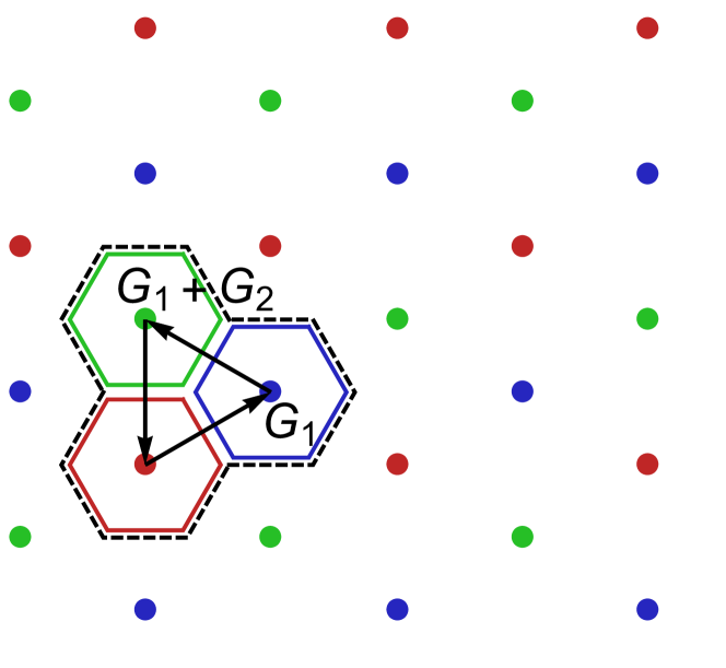
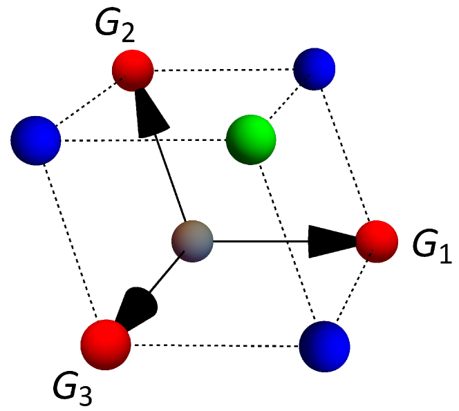
Right: reciprocal lattice of silicon. In the case of silicon there are four possible axial phases and hence four colors for the reciprocal lattice sites, indicating the quadrupling of the Brillouin zone.
Having completed the warm up exercise of recovering know results for graphene in two spatial dimensions, we apply the same steps for silicon in three dimensions. In silicon the sites sit on lattice sites spanned by the basis vectors , , and , with Å. The reciprocal lattice vectors are , , and . The four vectors connecting sublattice to are , , , and .
The off-diagonal block matrix, whose dimension depends on how many orbitals we consider, is given by Eq. (2) of the main text with the index :
| (S5) |
where again we allowed generically for unequal values for the hoppings to the three nearest neighbors. The vectors and satisfy
| (S6) |
The Hamiltonian for silicon is therefore not periodic in , but instead is periodic up to the unitary transformation in Eq. (3) of the main text [repeated in Eq. (S3) for convenience], with . One can also check that , for , or equivalently, .
We then consider the walk in -space that was described in the main text, one that visits, in order, the points and back to . As explained in the main text, we start at a near but not at the point, to avoid passing through lines of degeneracy. At the end of the walk, the Hamiltonian returns to , but the eigenvector is rotated by the sequence of unitary operations
| (S7) |
The wavefunction changes sign upon returning from the walk, which requires that a -flux lines pierce the region enclosed by the walk. The flux lines required by the argument above are precisely those described in the main text, obtained via direct calculation of the Berry curvature in the model.
Appendix B Derivation of the effective Hamiltonian at the X points for the conduction band of silicon
Since electron energies at the X point come in degenerate pairs, the relevant physics of the two lowest conduction bands (that together are degenerate along the X-W direction) is to be described by an effective Hamiltonian. This can be done within the framework of degenerate perturbation theory[32].
In order to derive such an effective Hamiltonian we first diagonalize the full Hamiltonian of the model at the X point to identify pairs of eigenstates corresponding to five degenerate eigenvalues. Then we expand the Hamiltonian in the newfound basis to the second order in momentum (around the X point) to get a matrix of the type
| (S8) |
where label groups of degenerate sublevels and are by matrices with being the degeneracy of a given level group. represent matrix elements between two such groups of levels. In the case of the X point in silicon all degeneracies are twofold and , the enumeration starting from the lowest valence band. Then within second-order perturbation theory the effective Hamiltonian describing level group is given by
| (S9) |
Since and are groups of indices, we can also clarify the equation above and expand in a more explicit form using ordinary level indices and the full Hamiltonian as
| (S10) |
Performing this procedure for silicon numerically, we obtain the effective Hamiltonian for bands 5 and 6 that was presented in the main text,
| (S11) |