Engineering of Neutral Excitons and Exciton Complexes in Transition Metal Dichalcogenide Monolayers through External Dielectric Screening
Abstract
In order to fully exploit the potential of transition metal dichalcogenide monolayers (TMD-MLs), the well-controlled creation of atomically sharp lateral heterojunctions within these materials is highly desirable. A promising approach to create such heterojunctions is the local modulation of the electronic structure of an intrinsic TMD-ML via dielectric screening induced by its surrounding materials. For the realization of this non-invasive approach, an in-depth understanding of such dielectric effects is required. We report on the modulations of excitonic transitions in TMD-MLs through the effect of dielectric environments including low-k and high-k dielectric materials. We present absolute tuning ranges as large as meV for the optical band gaps of WSe2 and MoSe2 MLs and relative tuning ranges on the order of for the binding energies of neutral excitons in WSe2 MLs. The findings suggest the possibility to reduce the electronic band gap of WSe2 MLs by meV, paving the way towards dielectrically defined lateral heterojunctions.
-
May 2017
Keywords: Transition Metal Dichalcogenides, Tungsten Diselenide, Molybdenum Diselenide, Exciton, Trion, Photoluminescence, Reflectance, Dielectric Screening, Lateral Heterojunction, Two-Dimensional Material
1 Introduction
Since the discovery of graphene the class of atomically thin two-dimensional materials has been growing continuously[1, 2, 3, 4]. An exciting expansion of this class was done when transition metal dichalcogenide monolayers (TMD-MLs) were added to this material class [5]. In contrast to the semimetal graphene, TMD-MLs with the stoichiometric formula MX2, where M and X denote a transition metal atom (Mo, W, …) and a chalcogen atom (S, Se, …), respectively, are semiconductors with direct band gaps at the -points of the hexagonal Brillouin zone with energies in the range of visible light [6]. Additionally, the heavy metal ions, the reduced Coulomb screening in two dimensions and the lack of inversion symmetry in these materials result in a unique combination of giant exciton binding energies, large spin-orbit coupling, as well as a coupling between the spin and valley degrees of freedom at the two inequivalent -valleys that can be accessed optically [7, 8, 9].
Although there have been numerous reports on electronic and optoelectronic nanodevices made from TMD-MLs such as single-layer transistors, light-emitting diodes and photodetectors [10, 11, 12], there is a strong need to develop methods to create junctions. In analogy to well established semiconductor technology, where heterojunctions are the building blocks of most electronic and optoelectronic devices (e.g. laser diodes, HEMT transistors), the reliable creation of lateral heterojunctions within TMD-MLs would enable further development of next generation optoelectronic devices.
In analogy to three dimensional semiconductors where heterostructures are formed by interfacing materials of different chemical composition, lateral heterostructures of TMDs have been developed by introducing laterally varying stoichiometry [13, 14]. An alternative approach, which is unique to low dimensional materials, relies on the local modulation of screening of the ionic Coulomb potentials, as well as the Coulomb interaction between charge carriers, within the ML[15, 16] through a local variation of the relative permittivity of the ML’s direct environment, i.e. its substrate and cover material.
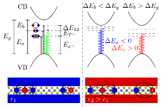
Fig. 1 depicts how externally induced screening changes both the electronic and optical band gaps of a TMD-ML. Both the electronic band gap, , and the binding energy of the neutral exciton, , in the monolayer are expected to decrease with an increasing relative permittivity of the surrounding dielectric [15, 16, 17, 18]. The sign of the change of the optical band gap, , depends on the relative change of these two quantities and can be probed optically by measuring the energy of free, neutral excitons. In addition to neutral excitons, charged exciton states (trions) with binding energies, , on the order of meV have been observed in TMD-MLs[19, 20, 21, 22]. Similarly to the binding energies of neutral excitons, the binding energies of trions in ML’s are expected to decrease with an increasing background relative permittivity[18]. Negatively charged trions are expected to be present in unbiased TMD-MLs, which are known to be unintentionally n-doped[19, 20, 21, 22].
A first experimental evidence for the tunability of excitonic properties in TMD-MLs through environment-induced dielectric screening has been the report of a room temperature blue shift of and in MoS2 MLs with an increasing relative permittivity of the non-ionic liquid with which the samples were covered[23]. More recently, an increase of the exciton Bohr radius in WSe2 MLs with an increasing background relative permittivity of the surrounding material of the ML has been observed[24]. In addition, a decrease of the exciton binding energy and the electronic band gap has been observed for WS2 MLs stacked with graphene[25].
In this work, we investigate different types of dielectrics as potential components of lateral heterostructure. We employ low temperature -photoluminescence, as well as reflectance measurements to study MoSe2 and WSe2 MLs. Our results show a red-shift of the optical band gaps, as well as a reduction of the binding energies of both the neutral exciton and the trion, with an increasing average relative permittivity of the ML’s surrounding. Estimates on the resulting changes of the electronic band gaps are made from the measured optical band gaps and exciton binding energies.
2 Experiments
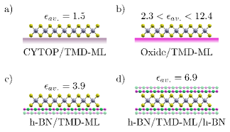
Mechanically exfoliated WSe2 and MoSe2 MLs have been prepared on different substrates. The substrates were required to be flat in order to minimize the strain and the number of defects introduced in the TMD-MLs. Only transparent wide band gap materials were used. The subsrates considered in this work can be separated into three types (fig. 2 a)-c)) according to their surface properties. The first type of substrate, namely CYTOP, is a low-k fluoropolymer, which is known for its chemical inertness and hydrophobicity. It is amorphous and transparent across a wide wavelength range and it features a very low relative permittivity for the entire frequency range. The second type are stable, transparent oxide substrates. Oxides offer a wide range of k-values but they are known to be hydrophilic. Hexagonal boron-nitride (h-BN) is a wide band gap layered material that can form van-der-Waals heterostructures with TMD-MLs. Similarly to CYTOP, h-BN is hydrophobic. A TMD-ML encapsulated by two hexagonal h-BN flakes was also included as a fourth dielectric environment (fig. 2 d)).
On a theoretical level, the effect of dielectric screening on excitonic properties is complex and non-analytic. Especially, an open question remains in which frequency domains the screening occurs. In our analysis, for the sake of simplicity, we identify the surrounding materials by their static dielectric constant. This represents a simplification, however, we emphasize that it does not change the conclusions from this work. A more detailed discussion of this point can be found in the Supporting Information. The average nominal relative permittivity of the environment, , ranged from for a TMD-ML on CYTOP to for a TMD-ML on LaAlO3. All the layers in contact with the MLs were at least several nanometers thick and, as a consequence, only the layers in direct contact with the TMD-ML are needed to be included in the analysis.
-photoluminescence maps, as well as optical reflectance measurements of all structures were acquired at K. While the former method only probes the emission energies of the ground states of neutral excitons and trions, absorption energies of the ground state, as well as of excited states, of the neutral exciton can be probed by the latter [26, 27]. We further analyze the impact of charging induced by the substrate or the cover material as the reason for the observed effects.
3 Results
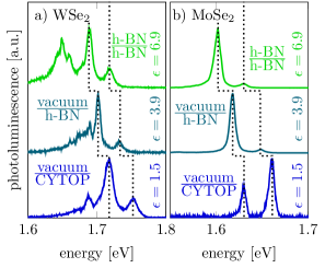
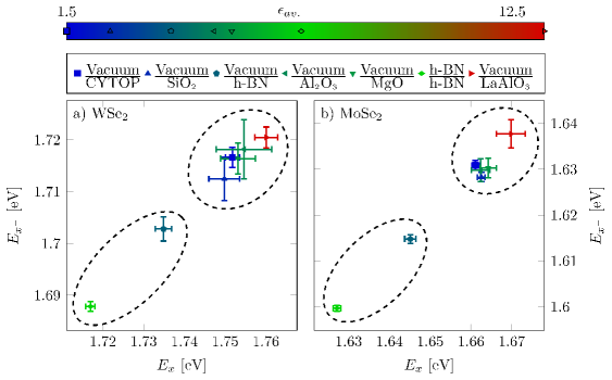
The emission energies of the neutral exciton and the trion of all structures shown in figure 2 have been measured in -photoluminescence experiments. Figure 3 shows photoluminescence spectra for three representative structures. The spectra contain signal from neutral exciton and trion recombination, as well as defect emission in the case of WSe2 MLs. The energy of these peaks shows a systematic shift with . Figure 4, summarizes the emission energies for both the neutral exciton and the trion for all measured structures. The data points are averaged over large areas in order to account for spatial variations of the peak positions. The trends in behaviour of WSe2 and MoSe2 MLs in different environments are very similar. The results for both TMD-MLs on SiO2, which is the most commonly used substrate, agree well with reports in the literature[28, 19]. There is a clear correlation in the positions of neutral exciton and trion peaks but there is no clear correlation with the nominal . Irrespective of the nominal relative permittivity of the substrate, the emission energies for MLs on CYTOP and for MLs on oxide substrates are very similar to each other and cluster around for WSe2 and at for MoSe2. We attribute this effect to the presence of water on the hydrophilic oxide surface preventing a direct contact between the substrate material and the TMD-MLs. Hexagonal ice has a relative permittivity below [29] and, thus, similar to that of CYTOP.
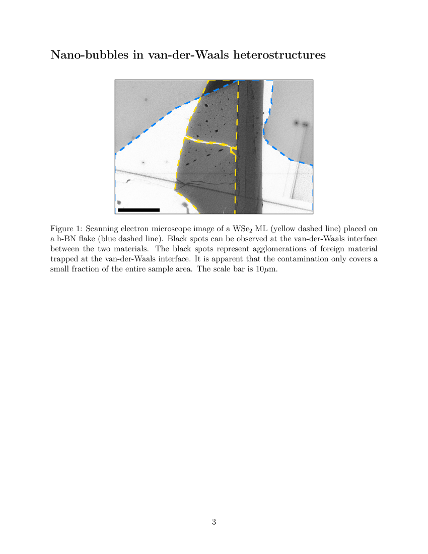
Even though the relative permittivity of h-BN is lower than that of some oxides, the emission energies of MLs on a h-BN substrate, as well as of MLs encapsulated in h-BN, show clearly observable red-shifts with respect to this cluster. For the neutral exciton, the red-shifts with respect to a ML on CYTOP are meV ( meV) and meV ( meV) for WSe2 (MoSe2) MLs on h-BN and encapsulated with h-BN, respectively. For the trion, the red-shifts with respect to a ML on CYTOP are meV ( meV) and meV ( meV) for WSe2 (MoSe2) MLs on h-BN and encapsulated with h-BN, respectively. It is well known that contamination is highly mobile in mechanically stacked van-der-Waals heterostructures clustering into so-called bubbles leaving behind large areas of clean interfaces (Supporting Info, fig. 1)[30]. Since this contamination covers only a very small fraction of the sample area, the photoluminescence emission from the clean interfaces is expected to dominate the measured signal.
The observed red-shifts for the h-BN structures imply that the electronic band gap is undergoing a larger absolute change than the exciton binding energies when increasing . These findings are in contrast to previously reported observations in room temperature measurements of MoS2 MLs in dielectric non-ionic liquids[23], but agree well with recent reflectance studies of TMD-MLs stacked with graphene[25].
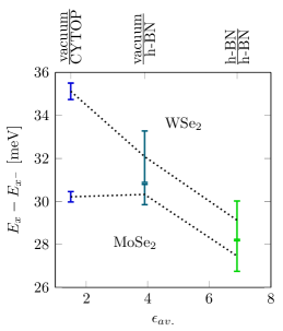
Figure 5 shows the evolution of the trion binding energy, determined from the difference between neutral exciton and trion energies, as a function of , for MoSe2 and WSe2. For WSe2 the trion binding energy decreases monotonically from meV for a ML on CYTOP to meV for a ML encapsulated in h-BN. This result is in good qualitative agreement with theoretical predictions [18]. In contrast, the trion binding energy of a MoSe2 ML is nearly identical for a ML on CYTOP and a ML on h-BN. However, similarly to WSe2, the trion binding energy of MoSe2 decreases from meV for a ML on h-BN to meV for a ML encapsulated between two h-BN flakes. The small change between the trion binding energy of a MoSe2 ML on CYTOP and a MoSe2 ML on h-BN is still under investigation. A possible explanation may be a positive polarity of the trion for a ML on CYTOP, which, having a lower binding energy than negatively charged trions would cancel out the effect of the reduced screening [28]. An indication for a different background charge for the ML on CYTOP is the different exciton-trion ratio observed in this structure (fig. 3). The trion binding energies are determined as the average difference between the exciton and trion emission energies and the standard deviations shown in figure 5 are up to five times lower than those determined for the exciton and trion emission energies themselves (fig. 4). This lower spatial fluctuation of the trion binding energy, indicates the robustness of excitonic binding energies against perturbations such as strain, as expected from theoretical studies [31]. Trion binding energies could thus be potentially used as a sensitive probe of surface state of transition metal dichalcogenide monolayers, providing a non-invasive alternative to the use of water droplets [32].
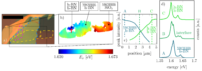
Changes of the optical band gap of TMD-MLs with spatially modulated are shown in figure 6 for a single MoSe2 ML. The sample is prepared by placing the ML on an interface between SiO2 and hBN and partially covering it with a hBN layer. While small variations of within a region of constant are present, the correlation of with the local of the TMD-ML is clear. The residual variations within each region are most likely due to strain variations, which are known to change the ML’s electronic band gap[33]. A line profile across the boundary, that separates the part of the monolayer encapsulated in h-BN from the uncovered part on h-BN is shown in figure 6 c). In the line profile, it can be seen that the change of the optical band gap is observed over a distance of approximately m, which is the size of the laser spot in our measurements. Consequently, the band gap change is much more abrupt than the radius of the laser spot, which agrees well with theoretical predictions of the transition occuring across only a few crystal unit cells[15]. A representative spectrum from the interface between the two areas is shown in figure 6 d). It is a clear superposition of the peaks characteristics of each of the two areas. A line profile crossing the boundary between the ML area on h-BN and the ML area on SiO2 cannot be analyzed, as there is no smooth transition of the photoluminescence signal observable. The height step between the two areas, which introduces strain or defects in the ML is most likely responsible for the distortions. The comparison between the two discussed interfaces demonstrates that the formation of well-defined, abrupt lateral heterostructures requires a change of the relative permittivity on a flat substrate.
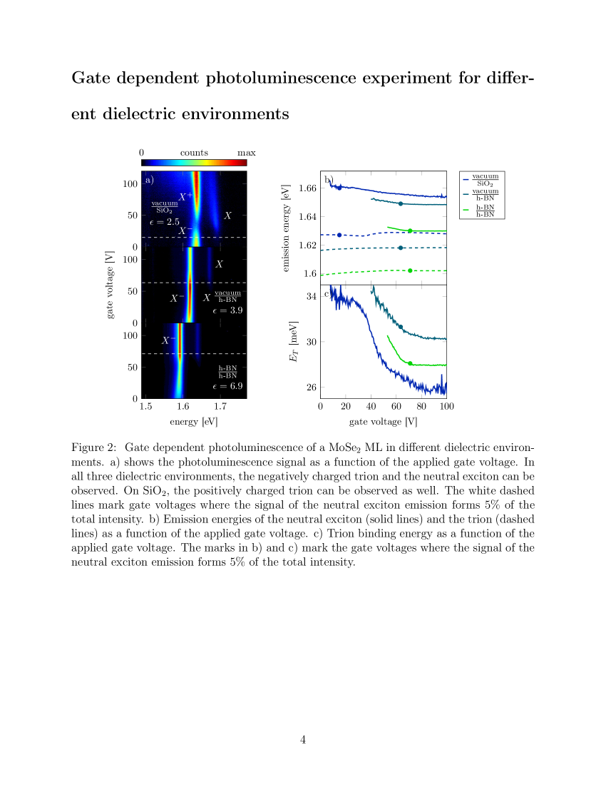
Screening of Coulomb interactions at high carrier densities in TMD-MLs can lead to shifts in the exciton energies [34]. Such charges can be unintentionally introduced, for example, via substrate doping[35]. In order to evaluate the possible role of doping we performed gate dependent photoluminescence experiments by contacting the device shown in fig. 6 with graphene as a contact. The results of the gate dependent photoluminescence experiments are shown in the Supporting Information (Supporting Information, Figure 2). It is apparent that, although the emission energies of both the neutral exciton and the trion are undergoing small changes if the gate voltage is changed, they are much smaller than the effect of the dielectric environment. In addition, different binding energies for negatively and positively charged trions can be seen, supporting the suggestion that the measured trion binding energy for a MoSe2 ML on CYTOP can be explained by a positive polarity of the trion in this structure.
So far, the discussion has been limited to photoluminescence experiments, the results of which are of importance mainly for the design of new ultra-thin light sources with a tailored emission energy. However, the electronic band gap is also affected by the dielectric screening and understanding of the interplay between the two values may be of importance for trion confinement, as well as confinement in electronic devices. For this reason, we performed optical reflectance measurements which probe Rydberg series of the neutral exciton. The energy splittings in the Rydberg series are related to the exciton binding energy, the latter combined with optical band gap yielding an estimate of the electronic band gap[26]. The reflectance measurements were limited to WSe2 MLs. The excited states of the neutral exciton overlap with the B-exciton in MoSe2 MLs and, thus, cannot be measured[37].
Due to the optical transparency of TMD-MLs, the effect of light reflection from the ML constitutes as small part of the total reflections from the sample. For this reason, reflectance contrast measurements need to be performed on such structures. The reflectance contrast is then given by , where and denote the reflectance from the ML region and the reflectance from a reference region without a ML structure, respectively. In order to make the features of the excited exciton states more pronounced, it is convenient to plot the energy derivative of the reflectance contrast, [26].
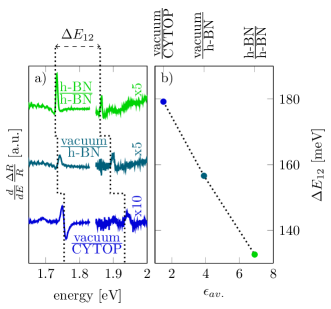
Figure 7 shows the energy derivative of the reflectance contrast of WSe2 MLs for three measured samples together with the evolution of the energy splitting between the ground state and the first excited state of the neutral exciton, , as a function of . As in the photoluminescence experiments, the optical band gap is red-shifted. In addition, it is apparent that , and hence , is decreasing with an increasing relative permittivity of the surrounding material of the ML. decreases monotonically from approximately meV for a WSe2 ML on CYTOP to almost meV for a WSe2 ML encapsulated by two h-BN flakes. Theoretical quasi two-dimensional calculations predict a relative change of for the exciton binding energy when moving from a MoS2 ML on h-BN to a MoS2 ML encapsulated with h-BN, which agrees well with the measured relative change in of [17].
For MoS2 and WS2 MLs on SiO2, it has been shown that , deviating from a classic hydrogenic model in three-dimensional semiconductors with [26, 27]. With the assumption that this scaling factor is independent of the dielectric surrounding of the TMD-ML, we estimate the absolute reduction in the exciton binding energy to be on the order of meV when replacing the CYTOP substrate with h-BN encapsulation. A decrease of meV, which is more than two times larger than the thermal energy at room temperature is obtained by combining the measured shift in the optical band gap with the reduction of the electron binding energy.
4 Conclusions
We have shown that h-BN is a suitable cladding material to tune the optical band gap of TMD-MLs whereas oxide substrates, irrespective of their relative permittivisties, do not lead to a significant change in the optical band gaps of TMD-MLs.
A reduction of the optical band gaps of MoSe2 and WSe2 MLs by meV was measured between the uncovered ML placed on a CYTOP substrate and a ML encapsulated in h-BN. In addition, a relative change of the exciton binding energy for WSe2 MLs of approximately was indirectly measured, which leads to an estimated reduction of the electronic band gap of WSe2 MLs by meV, when comparing uncovered MLs on a CYTOP substrate to a ML encapsulated in h-BN.
The energies of optical transition obtained in this work have been probed on the time scale of the exciton lifetime. It would be interesting to compare our results for the electronic band gap with scanning tunneling microscopy experiments, which probe the electronic band gap in the static limit.
We have shown that formation of optical lateral heterostructure purely by local variation of screening in three dimensions will require a control of the substrate flatness as well as substrate induced charge state. The latter is important to avoid energy transfer between excitons and trions of different parts of the heterostructure.
In the heterojunction studied in this work (see fig. 6), the change from one region to another region was abrupt on the scale of the probe beam. Therefore, techniques with a better spatial resolution need to be developed in order to study dielectric effects on smaller length scales.
Our findings pave the way towards the creation of controlled lateral heterostructures, which are required as building blocks for next generation electronic and optoelectronic devices.
5 Acknowledgements
S. B. would like to thank Tony Heinz, Alexey Chernikov and Archana Raja for fruitful discussions and helpful advices.
6 References
References
- [1] Novoselov K S, Geim A K, Morozov S V, Jiang D, Zhang Y, Dubonos S V, Grigorieva I V and Firsov A A 2004 Science 306 666–669
- [2] Li L, Yu Y, Ye G J, Ge Q, Ou X, Wu H, Feng D, Chen X H and Zhang Y 2014 Nature Nanotechnology 9 372–377
- [3] Vogt P, Padova P D, Quaresima C, Avila J, Frantzeskakis E, Asensio M C, Resta A, Ealet B and Lay G L 2012 Phys. Rev. Lett. 108 155501
- [4] Dávila M E, Xian L, Cahangirov S, Rubio A and Lay G L 2014 New Journal of Physics 16 095002
- [5] Mak K F, Lee C, Hone J, Shan J and Heinz T F 2010 Phys. Rev. Lett. 105 136805
- [6] Rasmussen F A and Thygesen K S 2015 J. Phys. Chem. C 119 (23) 13169–13183
- [7] Ugeda M M, Bradley A J, Shi S F, da Jornada F H, Zhang Y, Qiu D Y, Ruan W, Mo S K, Hussain Z, Shen Z X, Wang F, Louie S G and Crommie M F 2014 Nature Materials 13 1091–1095
- [8] Cao T, Wang G, Han W, Ye H, Zhu C, Shi J, Niu Q, Tan P, Wang E, Liu B and Feng J 2012 Nature Communications 3
- [9] Xiao D, Liu G B, Feng W, Xu X, and Yao W 2012 Phys. Rev. Lett. 108 196802
- [10] Radisavljevic B, Radenovic A, Brivio J, Giacometti V and Kis A 2011 Nature Nanotechnology 6 147–150
- [11] Ross J S, Klement P, Jones A M, Ghimire N J, Yan J, Mandrus D G, Taniguchi T, Watanabe K, Kitamura K, Yao W, Cobden D H and Xu X 2014 Nature Nanotechnology 9 268–272
- [12] Lopez-Sanchez O, Lembke D, Kayci M, Radenovic A and Kis A 2013 Nature Nanotechnology 8 497–501
- [13] Huang C, Wu S, Sanchez A M, Peters J J P, Beanland R, Ross J S, Rivera P, Yao W, Cobden D H and Xu X 2014 Nature Materials 13 1096–1101
- [14] Mahjouri-Samani M, Lin M W, Wang K, Lupini A R, Lee J, Basile L, Boulesbaa A, Rouleau C M, Puretzky A A, Ivanov I N, Xiao K, Yoon M and Geohegan D B 2015 Nature Communications 6 7749
- [15] Rösner M, Steinke C, Lorke M, Gies C, Jahnke F and Wehling T O 2016 Nano Lett. 16 2322–2327
- [16] Ryou J, Kim Y S, KC S and Cho K 2016 Scientific Reports 6 29184
- [17] Latini S, Olsen T and Thygesen K S 2015 Phys. Rev. B 92 245123
- [18] Kylänpää I and Komsa H P 2015 Phys. Rev. B 92 205418
- [19] Ross J S, Wu S, Yu H, Ghimire N J, Jones A M, Aivazian G, Yan J, Mandrus D G, Xiao D, Yao W and Xu X 2013 Nature Communications 4 1474
- [20] Mak K F, He K, Shan J and Heinz T F 2012 Nature Nanotechnology 7 494–498
- [21] Wang G, Bouet L, Lagarde D, Vidal M, Balocchi A, Amand T, Marie X and Urbaszek B 2014 Phys. Rev. B 90 075413
- [22] Plechinger G, Nagler P, Kraus J, Paradiso N, Strunk C, Schüller C and Korn T 2015 physica status solidi (RRL) 9 457–461
- [23] Lin Y, Ling X, Yu L, Huang S, Hsu A L, Lee Y H, Kong J and Palacios M S D T 2014 Nano Lett. 14 5569–5576
- [24] Stier A V, Wilson N P, Clark G, Xu X and Crooker S A 2016 Nano Lett. 16 7054–7060
- [25] Raja A, Chaves A, Yu J, Arefe G, Hill H M, Rigosi A F, Berkelbach T C, Nagler P, Schüller C, Korn T, Nuckolls C, Hone J, Brus L E, Heinz T F, Reichman D R and Chernikov A 2017 Nature Communications 8 15251
- [26] Chernikov A, Berkelbach T C, Hill H M, Rigosi A, Li Y, Aslan O B, Reichman D R and Heinz M S H T F 2014 Phys. Rev. Lett. 113 076802
- [27] Hill H M, Rigosi A F, Roquelet C, Chernikov A, Berkelbach T C, Reichman D R, Hybertsen M S, Brusand L E and Heinz T F 2015 Nano Lett. 15 2992–2997
- [28] Jones A, Yu H, Ghimire N J, Wu S, Aivazian G, Ross J S, Zhao B, Yan J, Mandrus D G, Xiao D, Yao W and Xu X 2013 Nature Nanotechnology 8 634–638
- [29] Kobayashl K 1982 J. Phys. Chem. 87 4317–4321
- [30] Haigh S J, Gholinia A, Jalil R, Romani S, Britnell L, Elias D C, Novoselov K S, Ponomarenko L A, Geim A K and Gorbachev R 2012 Nature Materials 11 764–767
- [31] abd Hui Pan H S, Zhang Y W and Yakobson B I 2013 Phys. Rev. B 87 155304
- [32] Chow P K, Singh E, Viana B C, Gao† J, Luo J, Li J, Lin Z, Elías A L, Shi Y, Wang Z, Terrones M and Koratkar N 2015 ACS Nano 9 3023–3031
- [33] Johari P and Shenoy V B 2012 ACS Nano 6 5449–5456
- [34] Steinhoff A, Rösner M, Jahnke F and nd C Gies T O W 2014 Nano Lett. 14 3743–3748
- [35] Sercombe D, Schwarz S, Pozo-Zamudio O D, Liu F, Robinson B J, Chekhovich E A, Tartakovskii I I, Kolosov O and Tartakovskii A I 2013 Scientific Reports 3 3489
- [36] 2012 Multilayer thin film optics calculator http://sjbyrnes.com/
- [37] Wang G, Gerber I C, Bouet L, Lagarde D, Balocchi A, Vidal M, Amand T, Marie X and Urbaszek B 2015 2D Materials 2 4