Understanding Reduced-Voltage Operation in Modern DRAM
Chips:
Characterization, Analysis, and Mechanisms
Abstract.
The energy consumption of DRAM is a critical concern in modern computing systems. Improvements in manufacturing process technology have allowed DRAM vendors to lower the DRAM supply voltage conservatively, which reduces some of the DRAM energy consumption. We would like to reduce the DRAM supply voltage more aggressively, to further reduce energy. Aggressive supply voltage reduction requires a thorough understanding of the effect voltage scaling has on DRAM access latency and DRAM reliability.
In this paper, we take a comprehensive approach to understanding and exploiting the latency and reliability characteristics of modern DRAM when the supply voltage is lowered below the nominal voltage level specified by DRAM standards. Using an FPGA-based testing platform, we perform an experimental study of 124 real DDR3L (low-voltage) DRAM chips manufactured recently by three major DRAM vendors. We find that reducing the supply voltage below a certain point introduces bit errors in the data, and we comprehensively characterize the behavior of these errors. We discover that these errors can be avoided by increasing the latency of three major DRAM operations (activation, restoration, and precharge). We perform detailed DRAM circuit simulations to validate and explain our experimental findings. We also characterize the various relationships between reduced supply voltage and error locations, stored data patterns, DRAM temperature, and data retention.
Based on our observations, we propose a new DRAM energy reduction mechanism, called Voltron. The key idea of Voltron is to use a performance model to determine by how much we can reduce the supply voltage without introducing errors and without exceeding a user-specified threshold for performance loss. Our evaluations show that Voltron reduces the average DRAM and system energy consumption by 10.5% and 7.3%, respectively, while limiting the average system performance loss to only 1.8%, for a variety of memory-intensive quad-core workloads. We also show that Voltron significantly outperforms prior dynamic voltage and frequency scaling mechanisms for DRAM.
1. Introduction
In a wide range of modern computing systems, spanning from warehouse-scale data centers to mobile platforms, energy consumption is a first-order concern (hoelzle-book2009, ; ibm-power7, ; deng-asplos2011, ; david-icac2011, ; malladi-isca2012, ; yoon-isca2012, ; choi-memcon2013, ; superfri, ; mutlu-imw2013, ). In these systems, the energy consumed by the DRAM-based main memory system constitutes a significant fraction of the total energy. For example, experimental studies of production systems have shown that DRAM consumes 40% of the total energy in servers (hoelzle-book2009, ; ibmpower7-hpca, ) and 40% of the total power in graphics cards (paul-isca2015, ).
The energy consumed by DRAM is correlated with the supply voltage used within the DRAM chips. The supply voltage is distributed to the two major components within DRAM: the DRAM array and the peripheral circuitry (vogelsang-micro2010, ; lee-thesis2016, ). The DRAM array consists of thousands of capacitor-based DRAM cells, which store data as charge within the capacitor. Accessing data stored in the DRAM array requires a DRAM chip to perform a series of fundamental operations: activation, restoration, and precharge.111We explain the detail of each of these operations in Section 2. A memory controller orchestrates each of the DRAM operations while obeying the DRAM timing parameters. On the other hand, the peripheral circuitry consists of control logic and I/O drivers that connect the DRAM array to the memory channel, which is responsible for transferring commands and data between the memory controller and the DRAM chip. Since the DRAM supply voltage is distributed to both the DRAM array and the peripheral circuitry, changing the supply voltage would affect the energy consumption of both components in the entire DRAM chip.
To reduce the energy consumed by DRAM, vendors have developed low-voltage variants of DDR (Double Data Rate) memory, such as LPDDR4 (Low-Power DDR4) (jedec-lpddr4, ) and DDR3L (DDR3 Low-voltage) (jedec-ddr3l, ). For example, in DDR3L, the internal architecture remains the same as DDR3 DRAM, but vendors lower the nominal supply voltage to both the DRAM array and the peripheral circuitry via improvements in manufacturing process technology. In this work, we would like to reduce DRAM energy by further reducing DRAM supply voltage. Vendors choose a conservatively high supply voltage, to provide a guardband that allows DRAM chips with the worst-case process variation to operate without errors under the worst-case operating conditions (david-icac2011, ). The exact amount of supply voltage guardband varies across chips, and lowering the voltage below the guardband can result in erroneous or even undefined behavior. Therefore, we need to understand how DRAM chips behave during reduced-voltage operation. To our knowledge, no previously published work examines the effect of using a wide range of different supply voltage values on the reliability, latency, and retention characteristics of DRAM chips.
Our goal in this work is to (i) characterize and understand the relationship between supply voltage reduction and various characteristics of DRAM, including DRAM reliability, latency, and data retention; and (ii) use the insights derived from this characterization and understanding to design a new mechanism that can aggressively lower the supply voltage to reduce DRAM energy consumption while keeping performance loss under a bound. To this end, we build an FPGA-based testing platform that allows us to tune the DRAM supply voltage (hassan-hpca2017, ). Using this testing platform, we perform experiments on 124 real DDR3L DRAM chips (jedec-ddr3l, ) from three major vendors, contained within 31 dual in-line memory modules (DIMMs). Our comprehensive experimental characterization provides four major observations on how DRAM latency, reliability, and data retention time are affected by reduced supply voltage.
First, we observe that we can reliably access data when DRAM supply voltage is lowered below the nominal voltage, until a certain voltage value, , which is the minimum voltage level at which no bit errors occur. Furthermore, we find that we can reduce the voltage below to attain further energy savings, but that errors start occurring in some of the data read from memory. As we drop the voltage further below , the number of erroneous bits of data increases exponentially with the voltage drop.
Second, we observe that while reducing the voltage below introduces bit errors in the data, we can prevent these errors if we increase the latency of the three fundamental DRAM operations (activation, restoration, and precharge). When the supply voltage is reduced, the capacitor charge takes a longer time to change, thereby causing these DRAM operations to become slower to complete. Errors are introduced into the data when the memory controller does not account for this slowdown in the DRAM operations. We find that if the memory controller allocates extra time for these operations to finish when the supply voltage is below , errors no longer occur. We validate, analyze, and explain this behavior using detailed circuit-level simulations.
Third, we observe that when only a small number of errors occur due to reduced supply voltage, these errors tend to cluster physically in certain regions of a DRAM chip, as opposed to being randomly distributed throughout the chip. This observation implies that when we reduce the supply voltage to the DRAM array, we need to increase the fundamental operation latencies for only the regions where errors can occur.
Fourth, we observe that reducing the supply voltage does not impact the data retention guarantees of DRAM. Commodity DRAM chips guarantee that all cells can safely retain data for 64ms, after which the cells are refreshed to replenish charge that leaks out of the capacitors. Even when we reduce the supply voltage, the rate at which charge leaks from the capacitors is so slow that no data is lost during the 64ms refresh interval at 20 and 70 ambient temperature.
Based on our experimental observations, we propose a new low-cost DRAM energy reduction mechanism called Voltron. The key idea of Voltron is to use a performance model to determine by how much we can reduce the DRAM array voltage at runtime without introducing errors and without exceeding a user-specified threshold for acceptable performance loss. Voltron consists of two components: array voltage scaling and performance-aware voltage control.
Array voltage scaling leverages minimal hardware modifications within DRAM to reduce the voltage of only the DRAM array, without affecting the voltage of the peripheral circuitry. If Voltron were to reduce the voltage of the peripheral circuitry, we would have to reduce the operating frequency of DRAM. This is because the maximum operating frequency of DRAM is a function of the peripheral circuitry voltage (david-icac2011, ). A reduction in the operating frequency reduces the memory data throughput, which can significantly harm the performance of applications that require high memory bandwidth, as we demonstrate in this paper.
Performance-aware voltage control uses performance counters within the processor to build a piecewise linear model of how the performance of an application decreases as the DRAM array supply voltage is lowered (due to longer operation latency to prevent errors), and uses the model to select a supply voltage that keeps performance above a user/system-specified performance target.
Our evaluations of Voltron show that it significantly reduces both DRAM and system energy consumption, at the expense of very modest performance degradation. For example, at an average performance loss of only 1.8% over seven memory-intensive quad-core workloads from SPEC2006, Voltron reduces DRAM energy consumption by an average of 10.5%, which translates to an overall system energy consumption of 7.3%. We also show that Voltron effectively saves DRAM and system energy on even non-memory-intensive applications, with very little performance impact.
This work makes the following major contributions:
-
We perform the first detailed experimental characterization of how the reliability and latency of modern DRAM chips are affected when the supply voltage is lowered below the nominal voltage level. We comprehensively test and analyze 124 real DRAM chips from three major DRAM vendors. Our characterization reveals four new major observations, which can be useful for developing new mechanisms that improve or better trade off between DRAM energy/power, latency, and/or reliability.
-
We experimentally demonstrate that reducing the supply voltage below a certain point introduces bit errors in the data read from DRAM. We show that we can avoid these bit errors by increasing the DRAM access latency when the supply voltage is reduced.
-
We propose Voltron, a mechanism that (i) reduces the supply voltage to only the DRAM array without affecting the peripheral circuitry, and (ii) uses a performance model to select a voltage that does not degrade performance beyond a chosen threshold. We show that Voltron is effective at improving system energy consumption, with only a small impact on performance.
-
We open-source our FPGA-based experimental characterization infrastructure and DRAM circuit simulation infrastructure, used in this paper, for evaluating reduced-voltage operation (volt-github, ).
2. Background and Motivation
In this section, we first provide necessary DRAM background and terminology. We then discuss related work on reducing the voltage and/or frequency of DRAM, to motivate the need for our study.
2.1. DRAM Organization
Figure 1(a) shows a high-level overview of a modern memory system organization. A processor (CPU) is connected to a DRAM module via a memory channel, which is a bus used to transfer data and commands between the processor and DRAM. A DRAM module is also called a dual in-line memory module (DIMM) and it consists of multiple DRAM chips, which are controlled together.222In this paper, we study DIMMs that contain a single rank (i.e., a group of chips in a single DIMM that operate in lockstep). Within each DRAM chip, illustrated in Figure 1(b), we categorize the internal components into two broad categories: (i) the DRAM array, which consists of multiple banks of DRAM cells organized into rows and columns, and (ii) peripheral circuitry, which consists of the circuits that sit outside of the DRAM array. For a more detailed view of the components in a DRAM chip, we refer the reader to prior works (vogelsang-micro2010, ; kim-isca2012, ; lee-hpca2013, ; liu-isca2012, ; lee-hpca2015, ; hassan-hpca2016, ; chang2016low, ; chang-thesis2017, ; lee-thesis2016, ; kim-thesis2015, ; lee-sigmetrics2017, ; chang-sigmetrics2016, ; lee-pact2015, ; seshadri-micro2013, ; seshadri-arxiv2016, ; lee-arxiv2016, ; chang-hpca2014, ; seshadri-thesis2016, ; seshadri-micro2015, ).

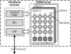
A DRAM array is divided into multiple banks (typically eight in DDR3 DRAM (jedec-ddr3l, ; jedec-ddr3, )) that can process DRAM commands independently from each other to increase parallelism. A bank contains a 2-dimensional array of DRAM cells. Each cell uses a capacitor to store a single bit of data. Each array of cells is connected to a row of sense amplifiers via vertical wires, called bitlines. This row of sense amplifiers is called the row buffer. The row buffer senses the data stored in one row of DRAM cells and serves as a temporary buffer for the data. A typical row in a DRAM module (i.e., across all of the DRAM chips in the module) is 8KB wide, comprising 128 64-byte cache lines.
The peripheral circuitry has three major components. First, the I/O component is used to receive commands or transfer data between the DRAM chip and the processor via the memory channel. Second, a typical DRAM chip uses a delay-lock loop (DLL) to synchronize its data signal with the external clock to coordinate data transfers on the memory channel. Third, the control logic decodes DRAM commands sent across the memory channel and selects the row and column of cells to read data from or write data into.
2.2. Accessing Data in DRAM
To access data stored in DRAM, the memory controller (shown in Figure 1(a)) issues DRAM commands across the memory channel to the DRAM chips. Reading a cache line from DRAM requires three essential commands, as shown in Figure 2: ACTIVATE, READ, and PRECHARGE. Each command requires some time to complete, and the DRAM standard (jedec-ddr3l, ) defines the latency of the commands with a set of timing parameters. The memory controller can be programmed to obey different sets of timing parameters through the BIOS (intel-xmp, ; lee-hpca2015, ; amd-bkdg, ; amd-opteron, ).

Activate Command. To open the target row of data in the bank that contains the desired cache line, the memory controller first issues an ACTIVATE command to the target DRAM bank. During activation, the electrical charge stored in the target row starts to propagate to the row buffer. The charge propagation triggers the row buffer to latch the data stored in the row after some amount of time. The latency of an ACTIVATE command, or the activation latency, is defined as the minimum amount of time that is required to pass from the issue time of an ACTIVATE until the issue time of a column command (i.e., READ or WRITE). The timing parameter for the activation latency is called tRCD, as shown in Figure 2, and is typically set to 13ns in DDR3L (micronDDR3L_2Gb, ).
Since an activation drains charge from the target row’s cells to latch the cells’ data into the row buffer, the cells’ charge needs to be restored to prevent data loss. The row buffer performs charge restoration simultaneously with activation. Once the cells’ charge is fully restored, the row can be closed (and thus the DRAM array be prepared for the next access) by issuing a PRECHARGE command to the DRAM bank. The DRAM standard specifies the restoration latency as the minimum amount of time the controller must wait after ACTIVATE before issuing PRECHARGE. The timing parameter for restoration is called tRAS, as shown in Figure 2, and is typically set to 35ns in DDR3L (micronDDR3L_2Gb, ).
Read Command. Once the row data is latched in the row buffer after the ACTIVATE command, the memory controller issues a READ command. The row buffer contains multiple cache lines of data (8KB), and the READ command enables all DRAM chips in the DRAM module to select the desired cache line (64B) from the row buffer. Each DRAM chip on the module then drives ()th of the cache line from the row buffer to the I/O component within the peripheral circuitry. The peripheral circuitry of each chip then sends its ()th of the cache line across the memory channel to the memory controller. Note that the column access time to read and write the cache line is defined by the timing parameters tCL and tCWL, respectively, as shown in Figure 2. Unlike the activation latency (tRCD), tCL and tCWL are DRAM-internal timings that are determined by a clock inside DRAM (micronDDR3L_2Gb, ). Therefore, our FPGA-based experimental infrastructure (described in Section 3) cannot evaluate the effect of changing tCL and tCWL.
Precharge Command. After reading the data from the row buffer, the memory controller may contain a request that needs to access data from a different row within the same bank. To prepare the bank to service this request, the memory controller issues a PRECHARGE command to the bank, which closes the currently-activated row and resets the bank in preparation for the next ACTIVATE command. Because closing the activated row and resetting the bank takes some time, the standard specifies the precharge latency as the minimum amount of time the controller must wait for after issuing PRECHARGE before it issues an ACTIVATE. The timing parameter for precharge is called tRP, as shown in Figure 2, and is typically set to 13ns in DDR3L (micronDDR3L_2Gb, ).
2.3. Effect of DRAM Voltage and Frequency on Power Consumption
DRAM power is divided into dynamic and static power. Dynamic power is the power consumed by executing the access commands: ACTIVATE, PRECHARGE, and READ/WRITE. Each ACTIVATE and PRECHARGE consumes power in the DRAM array and the peripheral circuitry due to the activity in the DRAM array and control logic. Each READ/WRITE consumes power in the DRAM array by accessing data in the row buffer, and in the peripheral circuitry by driving data on the channel. On the other hand, static power is the power that is consumed regardless of the DRAM accesses, and it is mainly due to transistor leakage. DRAM power is governed by both the supply voltage and operating clock frequency: (david-icac2011, ). As shown in this equation, power consumption scales quadratically with supply voltage, and linearly with frequency.
DRAM supply voltage is distributed to both the DRAM array and the peripheral circuitry through respective power pins on the DRAM chip, dedicated separately to the DRAM array and the peripheral circuitry. We call the voltage supplied to the DRAM array, , and the voltage supplied to the peripheral circuitry, . Each DRAM standard requires a specific nominal supply voltage value, which depends on many factors, such as the architectural design and process technology. In this work, we focus on the widely used DDR3L DRAM design that requires a nominal supply voltage of 1.35V (jedec-ddr3l, ). To remain operational when the supply voltage is unstable, DRAM can tolerate a small amount of deviation from the nominal supply voltage. In particular, DDR3L DRAM is specified to operate with a supply voltage ranging from 1.283V to 1.45V (micronDDR3L_2Gb, ).
The DRAM channel frequency value of a DDR DRAM chip is typically specified using the channel data rate, measured in mega-transfers per second (MT/s). The size of each data transfer is dependent on the width of the data bus, which ranges from 4 to 16 bits for a DDR3L chip (micronDDR3L_2Gb, ). Since a modern DDR channel transfers data on both the positive and the negative clock edges (hence the term double data rate, or DDR), the channel frequency is half of the data rate. For example, a DDR data rate of 1600 MT/s means that the frequency is 800 MHz. To run the channel at a specified data rate, the peripheral circuitry requires a certain minimum voltage () for stable operation. As a result, the supply voltage scales directly (i.e., linearly) with DRAM frequency, and it determines the maximum operating frequency (deng-asplos2011, ; david-icac2011, ).
2.4. Memory Voltage and Frequency Scaling
One proposed approach to reducing memory energy consumption is to scale the voltage and/or the frequency of DRAM based on the observed memory channel utilization. We briefly describe two different ways of scaling frequency and/or voltage below.
Frequency Scaling. To enable the power reduction that comes with reduced DRAM frequency, prior works propose to apply dynamic frequency scaling (DFS) by adjusting the DRAM channel frequency based on the memory bandwidth demand from the DRAM channel (deng-asplos2011, ; deng-islped2012, ; deng-micro2012, ; paul-isca2015, ; begum-iiswc2015, ; sundriyal2016, ). A major consequence of lowering the frequency is the likely performance loss that occurs, as it takes a longer time to transfer data across the DRAM channel while operating at a lower frequency. The clocking logic within the peripheral circuitry requires a fixed number of DRAM cycles to transfer the data, since DRAM sends data on each edge of the clock cycle. For a 64-bit memory channel with a 64B cache line size, the transfer typically takes four DRAM cycles (jedec-ddr3, ). Since lowering the frequency increases the time required for each cycle, the total amount of time spent on data transfer, in nanoseconds, increases accordingly. As a result, not only does memory latency increase, but also memory data throughput decreases, making DFS undesirable to use when the running workload’s memory bandwidth demand or memory latency sensitivity is high. The extra transfer latency from DRAM can also cause longer queuing times for requests waiting at the memory controller (lee-tech2010, ; ipek-isca08, ; kim-rtas2014, ; subramanian-iccd2014, ; subramanian-tpds2016, ; kim-rts2016, ), further exacerbating the performance loss and potentially delaying latency-critical applications (deng-asplos2011, ; david-icac2011, ).
Voltage and Frequency Scaling. While decreasing the channel frequency reduces the peripheral circuitry power and static power, it does not affect the dynamic power consumed by the operations performed on the DRAM array (i.e., activation, restoration, precharge). This is because DRAM array operations are asynchronous, i.e., independent of the channel frequency (micron-tr, ). As a result, these operations require a fixed time (in nanoseconds) to complete. For example, the activation latency in a DDR3L DRAM module is 13ns, regardless of the DRAM frequency (micronDDR3L_2Gb, ). If the channel frequency is doubled from 1066 MT/s to 2133 MT/s, the memory controller doubles the number of cycles for the ACTIVATE timing parameter (i.e., tRCD) (from 7 cycles to 14 cycles), to maintain the 13ns latency.
In order to reduce the dynamic power consumption of the DRAM array as well, prior work proposes dynamic voltage and frequency scaling (DVFS) for DRAM, which reduces the supply voltage along with the channel frequency (david-icac2011, ). This mechanism selects a DRAM frequency based on the current memory bandwidth utilization and finds the minimum operating voltage () for that frequency. is defined to be the lowest voltage that still provides “stable operation” for DRAM (i.e., no errors occur within the data). There are two significant limitations for this proposed DRAM DVFS mechanism. The first limitation is due to a lack of understanding of how voltage scaling affects the DRAM behavior. No prior work provides experimental characterization or analysis of the effect of reducing the DRAM supply voltage on latency, reliability, and data retention in real DRAM chips. As the DRAM behavior under reduced-voltage operation is unknown to satisfactorily maintain the latency and reliability of DRAM, the proposed DVFS mechanism (david-icac2011, ) can reduce supply voltage only very conservatively. The second limitation is that this prior work reduces the supply voltage only when it reduces the channel frequency, since a lower channel frequency requires a lower supply voltage for stable operation. As a result, DRAM DVFS results in the same performance issues experienced by the DRAM DFS mechanisms. In Section 6.3, we evaluate the main prior work (david-icac2011, ) on memory DVFS to quantitatively demonstrate its benefits and limitations.
2.5. Our Goal
The goal of this work is to (i) experimentally characterize and analyze real modern DRAM chips operating at different supply voltage levels, in order to develop a solid and thorough understanding of how reduced-voltage operation affects latency, reliability, and data retention in DRAM; and (ii) develop a mechanism that can reduce DRAM energy consumption by reducing DRAM voltage, without having to sacrifice memory data throughput, based on the insights obtained from comprehensive experimental characterization. Understanding how DRAM characteristics change at different voltage levels is imperative not only for enabling memory DVFS in real systems, but also for developing other low-power and low-energy DRAM designs that can effectively reduce the DRAM voltage. We experimentally analyze the effect of reducing supply voltage of modern DRAM chips in Section 4, and introduce our proposed new mechanism for reducing DRAM energy in Section 5.
3. Experimental Methodology
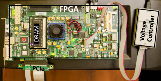
To study the behavior of real DRAM chips under reduced voltage, we build an FPGA-based infrastructure based on SoftMC (hassan-hpca2017, ), which allows us to have precise control over the DRAM modules. This method was used in many previous works (jung-memsys2016, ; jung-patmos2016, ; kim-isca2014, ; chang-sigmetrics2016, ; khan-sigmetrics2014, ; khan-dsn2016, ; hassan-hpca2017, ; lee-sigmetrics2017, ; mathew-rapido2017, ; lee-hpca2015, ; qureshi-dsn2015, ; khan2016case, ; lee-thesis2016, ; chang-thesis2017, ; kim-thesis2015, ; liu-isca2013, ) as an effective way to explore different DRAM characteristics (e.g., latency, reliability, and data retention time) that have not been known or exposed to the public by DRAM manufacturers. Our testing platform consists of a Xilinx ML605 FPGA board and a host PC that communicates with the FPGA via a PCIe bus (Figure 3). We adjust the supply voltage to the DRAM by using a USB interface adapter (ti-usb, ) that enables us to tune the power rail connected to the DRAM module directly. The power rail is connected to all the power pins of every chip on the module (as shown in Appendix A).
Characterized DRAM Modules. In total, we tested 31 DRAM DIMMs, comprising of 124 DDR3L (low-voltage) chips, from the three major DRAM chip vendors that hold more than 90% of the DRAM market share (bauer-mckinsey2016, ). Each chip has a 4Gb density. Thus, each of our DIMMs has a 2GB capacity. The DIMMs support up to a 1600 MT/s channel frequency. Due to our FPGA’s maximum operating frequency limitations, all of our tests are conducted at 800 MT/s. Note that the experiments we perform do not require us to adjust the channel frequency. Table 1 describes the relevant information about the tested DIMMs. Appendix E provides detailed information on each DIMM. Unless otherwise specified, we test our DIMMs at an ambient temperature of 201. We examine the effects of high ambient temperature (i.e., 70) in Section 4.5.
| Vendor | Total Number | Timing (ns) | Assembly |
|---|---|---|---|
| of Chips | (tRCD/tRP/tRAS) | Year | |
| A (10 DIMMs) | 40 | 13.75/13.75/35 | 2015-16 |
| B (12 DIMMs) | 48 | 13.75/13.75/35 | 2014-15 |
| C (9 DIMMs) | 36 | 13.75/13.75/35 | 2015 |
DRAM Tests. At a high level, we develop a test (Test 1) that writes/reads data to/from every row in the entire DIMM, for a given supply voltage. The test takes in several different input parameters: activation latency (tRCD), precharge latency (tRP), and data pattern. The goal of the test is to examine if any errors occur under the given supply voltage with the different input parameters.
In the test, we iteratively test two consecutive rows at a time. The two rows hold data that are the inverse of each other (i.e., and ). Reducing tRP lowers the amount of time the precharge unit has to reset the bitline voltage from either full voltage (bit value 1) or zero voltage (bit value 0) to half voltage. If tRP were reduced too much, the bitlines would float at some other intermediate voltage value between half voltage and full/zero voltage. As a result, the next activation can potentially start before the bitlines are fully precharged. If we were to use the same data pattern in both rows, the sense amplifier would require less time to sense the value during the next activation, as the bitline is already biased toward those values. By using the inverse of the data pattern in the row that is precharged for the next row that is activated, we ensure that the partially-precharged state of the bitlines does not unfairly favor the access to the next row (chang-sigmetrics2016, ). In total, we use three different groups of data patterns for our test: (0x00, 0xff), (0xaa, 0x33), and (0xcc, 0x55). Each specifies the and , placed in consecutive rows in the same bank.
4. Characterization of DRAM Under Reduced Voltage
In this section, we present our major observations from our detailed experimental characterization of 31 commodity DIMMs (124 chips) from three vendors, when the DIMMs operate under reduced supply voltage (i.e., below the nominal voltage level specified by the DRAM standard). First, we analyze the reliability of DRAM chips as we reduce the supply voltage without changing the DRAM access latency (Section 4.1). Our experiments are designed to identify if lowering the supply voltage induces bit errors (i.e., bit flips) in data. Second, we present our findings on the effect of increasing the activation and precharge latencies for DRAM operating under reduced supply voltage (Section 4.2). The purpose of this experiment is to understand the trade-off between access latencies (which impact performance) and the supply voltage of DRAM (which impacts energy consumption). We use detailed circuit-level DRAM simulations to validate and explain our observations on the relationship between access latency and supply voltage. Third, we examine the spatial locality of errors induced due to reduced-voltage operation (Section 4.3) and the distribution of errors in the data sent across the memory channel (Section 4.4). Fourth, we study the effect of temperature on reduced-voltage operation (Section 4.5). Fifth, we study the effect of reduced voltage on the data retention times within DRAM (Section 4.6). We present a summary of our findings in Section 4.7.
4.1. DRAM Reliability as Supply Voltage Decreases
We first study the reliability of DRAM chips under low voltage, which was not studied by prior works on DRAM voltage scaling (e.g., (david-icac2011, )). For these experiments, we use the minimum activation and precharge latencies that we experimentally determine to be reliable (i.e., they do not induce any errors) under the nominal voltage of 1.35V at 201 temperature. As shown in prior works (chang-sigmetrics2016, ; lee-hpca2015, ; chandrasekar-date2014, ; lee-sigmetrics2017, ; hassan-hpca2017, ; chang-thesis2017, ; lee-thesis2016, ; liu-isca2012, ; agrawal-hpca2014, ; qureshi-dsn2015, ; venkatesan-hpca2006, ; bhati-isca2015, ; lin-iccd2012, ; ohsawa-islped1998, ; patel-isca2017, ; khan-sigmetrics2014, ; khan-dsn2016, ; khan2016case, ), DRAM manufacturers adopt a pessimistic standard latency that incorporates a large margin as a safeguard to ensure that each chip deployed in the field operates correctly under a wide range of conditions. Examples of these conditions include process variation, which causes some chips or some cells within a chip to be slower than others, or high operating temperatures, which can affect the time required to perform various operations within DRAM. Since our goal is to understand how the inherent DRAM latencies vary with voltage, we conduct our experiments without such an excessive margin. We identify that the reliable tRCD and tRP latencies are both 10ns (instead of the 13.75ns latency specified by the DRAM standard) at 20, which agree with the values reported by prior work on DRAM latency characterization (chang-sigmetrics2016, ; lee-hpca2015, ; chang-thesis2017, ; lee-thesis2016, ).
Using the reliable minimum latency values (i.e., 10ns for all of the DIMMs), we run Test 1, which accesses every bit within a DIMM at the granularity of a 64B cache line. In total, there are 32 million cache lines in a 2GB DIMM. We vary the supply voltage from the nominal voltage of 1.35V down to 1.20V, using a step size of 0.05V (50mV). Then, we change to a smaller step size of 0.025V (25mV), until we reach the lowest voltage at which the DIMM can operate reliably (i.e., without any errors) while employing the reliable minimum latency values. (We examine methods to further reduce the supply voltage in Section 4.2.) For each voltage step, we run 30 rounds of Test 1 for each DIMM. Figure 4 shows the fraction of cache lines that experience at least 1 bit of error (i.e., 1 bit flip) in each DIMM (represented by each curve), categorized based on vendor.
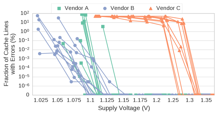
We make three observations. First, when each DIMM runs below a certain voltage level, errors start occurring. We refer to the minimum voltage level of each DIMM that allows error-free operation as . For example, most DIMMs from Vendor C have . Below , we observe errors because the fundamental DRAM array operations (i.e., activation, restoration, precharge) cannot fully complete within the time interval specified by the latency parameters (e.g., tRCD, tRAS) at low voltage. Second, not all cache lines exhibit errors for all supply voltage values below . Instead, the number of erroneous cache lines for each DIMM increases as we reduce the voltage further below . Specifically, Vendor A’s DIMMs experience a near-exponential increase in errors as the supply voltage reduces below . This is mainly due to the manufacturing process and architectural variation, which introduces strength and size variation across the different DRAM cells within a chip (kim-edl2009, ; li11, ; chang-sigmetrics2016, ; lee-sigmetrics2017, ; lee-hpca2015, ; chandrasekar-date2014, ; lee-thesis2016, ; kim-thesis2015, ; chang-thesis2017, ). Third, variation in exists not only across DIMMs from different vendors, but also across DIMMs from the same vendor. However, the variation across DIMMs from the same vendor is much smaller compared to cross-vendor variation, since the fabrication process and circuit designs can differ drastically across vendors. These results demonstrate that reducing voltage beyond , without altering the access latency, has a negative impact on DRAM reliability.
We also conduct an analysis of storing different data patterns on the error rate during reduced-voltage operation (see Appendix B). In summary, our results show that the data pattern does not have a consistent effect on the rate of errors induced by reduced-voltage operation. For most supply voltage values, the data pattern does not have a statistically significant effect on the error rate.
Source of Errors. To understand why errors occur in data as the supply voltage reduces below , we perform circuit-level SPICE simulations (nagel-spice, ; massobrio1993semiconductor, ), which reveal more detail on how the cell arrays operate. We develop a SPICE model of the DRAM array that uses a sense amplifier design from prior work (baker-dram, ) with the transistor model from the Predictive Technology Model (PTM) (ptm, ; zhao-isqed2006, ). Appendix C provides a detailed description of our SPICE simulation model, which we have open-sourced (volt-github, ).
We vary the supply voltage of the DRAM array () in our SPICE simulations from 1.35V to 0.90V. Figure 5 shows the bitline voltage during activation and precharge for different values. Times 0ns and 50ns correspond to when the DRAM receives the ACTIVATE and the PRECHARGE commands, respectively. An ACTIVATE causes the bitline voltage to increase from to in order to sense the stored data value of “1”. A PRECHARGE resets the bitline voltage back to in order to enable the issuing of a later ACTIVATE to another row within the same bank. In the figure, we mark the points where the bitline reaches the ready-to-access voltage, which we assume to be 75% of ; ready-to-precharge voltage, which we assume to be 98% of ; and ready-to-activate voltage, which we assume to be within 2% of . These points represent the minimum tRCD, tRAS, and tRP values, respectively, required for reliable DRAM operation. For readers who wish to understand the bitline voltage behavior in more detail, we refer them to recent works (lee-hpca2015, ; lee-hpca2013, ; hassan-hpca2016, ; lee-sigmetrics2017, ; lee-thesis2016, ) that provide extensive background on how the bitline voltage changes during the three DRAM operations.
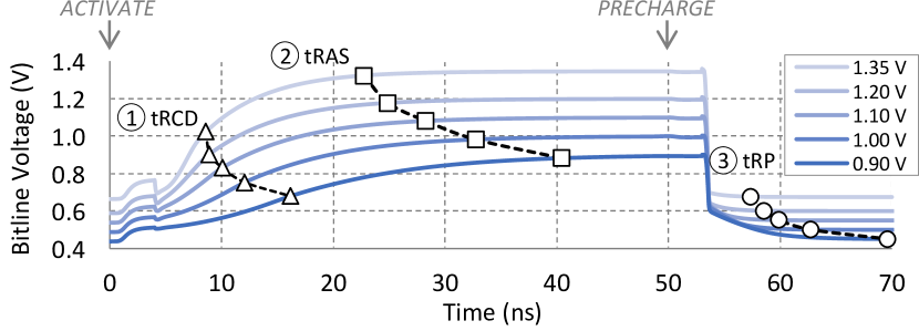
We make two observations from our SPICE simulations. First, we observe that the bitline voltage during activation increases at a different rate depending on the supply voltage of the DRAM array (). Thus, the supply voltage affects the latency of the three DRAM operations (activation, restoration, and precharge). When the nominal voltage level (1.35V) is used for , the time (tRCD) it takes for the sense amplifier to drive the bitline to the ready-to-access voltage level (75% of ) is much shorter than the time to do so at a lower . As decreases, the sense amplifier needs more time to latch in the data, increasing the activation latency. Similarly, the restoration latency (tRAS) and the precharge latency (tRP) increase as decreases.
Second, the latencies of the three fundamental DRAM array operations (i.e., activation, restoration, precharge) do not correlate with the channel (or clock) frequency (not shown in Figure 5). This is because these operations are clock-independent asynchronous operations that are a function of the cell capacitance, bitline capacitance, and (keeth-dram-tutorial, ).333In Appendix C, we show a detailed circuit schematic of a DRAM array that operates asynchronously, which forms the basis of our SPICE circuit simulation model (volt-github, ). As a result, the channel frequency is independent of the three fundamental DRAM operations.
Therefore, we hypothesize that DRAM errors occur at lower supply voltages because the three DRAM array operations have insufficient latency to fully complete at lower voltage levels. In the next section, we experimentally investigate the effect of increasing latency values as we vary the supply voltage on real DRAM chips.
4.2. Longer Access Latency Mitigates Voltage-Induced Errors
To confirm our hypothesis from Section 4.1 that a lower supply voltage requires a longer access latency, we test our DIMMs at supply voltages below the nominal voltage (1.35V) while incrementally increasing the activation and precharge latencies to be as high as 20ns (2x higher than the tested latency in Section 4.1). At each supply voltage value, we call the minimum required activation and precharge latencies that do not exhibit any errors and , respectively.
Figure 6 shows the distribution of (top row) and (bottom row) measured for all DIMMs across three vendors as we vary the supply voltage. Each circle represents a or value. A circle’s size indicates the DIMM population size, with bigger circles representing more DIMMs. The number above each circle indicates the fraction of DIMMs that work reliably at the specified voltage and latency. Also, we shade the range of potential and values. Since our infrastructure can adjust the latencies at a granularity of 2.5ns, a or value of 10ns is only an approximation of the minimum value, as the precise or falls between 7.5ns and 10ns. We make three major observations.


First, when the supply voltage falls below 444In Section 4.1, we define as the minimum voltage level of each DIMM that allows error-free operation. Table E in Appendix E shows the value we found for each DIMM., the tested DIMMs show that an increase of at least 2.5ns is needed for and to read data without errors. For example, some DIMMs require at least a 2.5ns increase of or to read data without errors at 1.100V, 1.125V, and 1.25V from Vendors A, B, and C, respectively. Since our testing platform can only identify the minimum latency at a granularity of 2.5ns (hassan-hpca2017, ), we use circuit-level simulations to obtain a more precise latency measurement of and (which we describe in the latter part of this section).
Second, DIMMs from different vendors exhibit very different behavior on how much and need to increase for reliable operation as supply voltage falls below . Compared to other vendors, many more of Vendor C’s DIMMs require higher and to operate at a lower . This is particularly the case for the precharge latency, . For instance, 60% of Vendor C’s DIMMs require a of 12.5ns to read data without errors at 1.25V, whereas this increase is not necessary at all for DIMMs from Vendor A, which all operate reliably at 1.15V. This reveals that different vendors may have different circuit architectures or manufacturing process technologies, which lead to variations in the additional latency required to compensate for a reduced in DIMMs.
Third, at very low supply voltages, not all of the DIMMs have valid and values less than or equal to 20ns that enable error-free operation of the DIMM. We see that the circle size gets smaller as the supply voltage reduces, indicating that the number of DIMMs that can operate reliably (even at higher latency) reduces. For example, Vendor A’s DIMMs can no longer operate reliably (i.e., error-free) when the voltage is below 1.1V. We tested a small subset of DIMMs with latencies of more than 50ns and found that these very high latencies still do not prevent errors from occurring. We hypothesize that this is because of signal integrity issues on the channel, causing bits to flip during data transfer at very low supply voltages.
We correlate our characterization results with our SPICE simulation results from Section 4.1, demonstrating that there is a direct relationship between supply voltage and access latency. This new observation on the trade-off between supply voltage and access latency is not discussed or demonstrated in prior work on DRAM voltage scaling (david-icac2011, ), where the access latency (in nanoseconds) remains fixed when performing memory DVFS. In conclusion, we demonstrate both experimentally and in circuit simulations that increasing the access latency (i.e., tRCD and tRP) allows us to lower the supply voltage while still reliably accessing data without errors.
Deriving More Precise Access Latency Values. One limitation of our experiments is that we cannot precisely measure the exact and values, due to the 2.5ns minimum latency granularity of our experimental framework (hassan-hpca2017, ). Furthermore, supply voltage is a continuous value, and it would take a prohibitively long time to study the supply voltage experimentally at a finer granularity. We address these limitations by enriching our experimental results with circuit-level DRAM SPICE simulations that model a DRAM array (see Appendix C for details of our circuit simulation model).
The SPICE simulation results highly depend on the specified transistor parameters (e.g., transistor width). To fit our SPICE results with our experimental results (for the supply voltage values that we studied experimentally), we manually adjust the transistor parameters until the simulated results fit within our measured range of latencies. Figure 7 shows the latencies reported for activation and precharge operations using our final SPICE model, based on the measured experimental data for Vendor B.
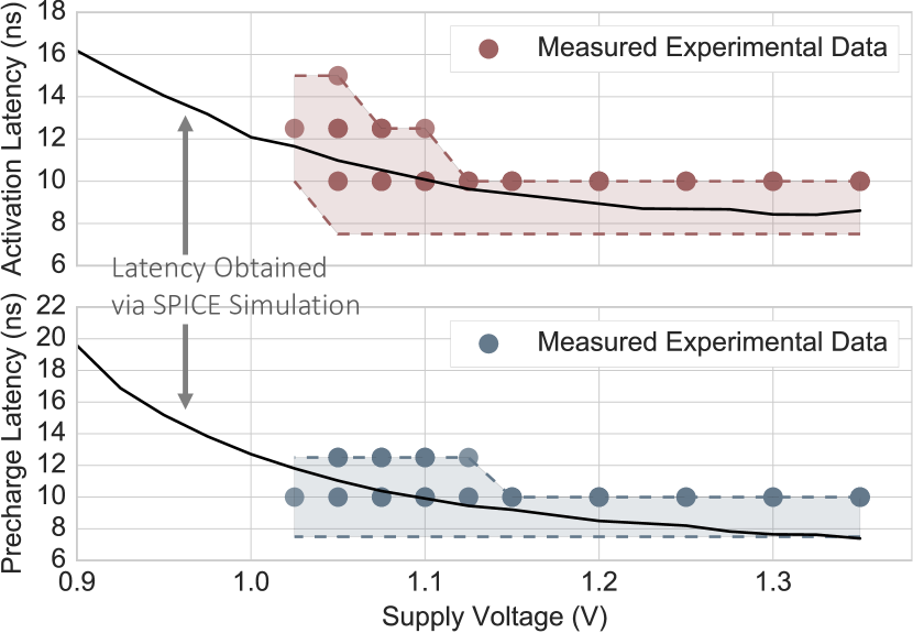
We make two major observations. First, we see that the SPICE simulation results fit within the range of latencies measured during our experimental characterization, confirming that our simulated circuit behaves close to the real DIMMs. As a result, our circuit model allows us to derive a more precise minimum latency for reliable operation than our experimental data.555The circuit model can further serve as a common framework for studying other characteristics of DRAM. Second, DRAM arrays can operate at a wide range of voltage values without experiencing errors. This aligns with our hypothesis that errors at very low supply voltages (e.g., 1V) occur during data transfers across the channel rather than during DRAM array operations. Therefore, our SPICE simulations not only validate our observation that a lower supply voltage requires longer access latency, but also provide us with a more precise reliable minimum operating latency estimate for a given supply voltage.
4.3. Spatial Locality of Errors
While reducing the supply voltage induces errors when the DRAM latency is not long enough, we also show that not all DRAM locations experience errors at all supply voltage levels. To understand the locality of the errors induced by a low supply voltage, we show the probability of each DRAM row in a DIMM experiencing at least one bit of error across all experiments. We present results for two representative DIMMs from two different vendors, as the observations from these two DIMMs are similar to those we make for the other tested DIMMs. Our results collected from each of the 31 DIMMs are publicly available (volt-github, ).
Figure 8 shows the probability of each row experiencing at least a one-bit error due to reduced voltage in the two representative DIMMs. For each DIMM, we choose the supply voltage when errors start appearing (i.e., the voltage level one step below ), and we do not increase the DRAM access latency (i.e., 10ns for both tRCD and tRP). The x-axis and y-axis indicate the bank number and row number (in thousands), respectively. Our tested DIMMs are divided into eight banks, and each bank consists of 32K rows of cells.666Additional results showing the error locations at different voltage levels are in Appendix D.
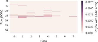
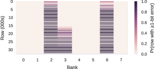
Our main observation is that errors tend to cluster at certain locations. For our representative DIMMs, we see that errors tend to cluster at certain rows across multiple banks for Vendor B. On the contrary, Vendor C’s DIMMs exhibit errors in certain banks but not in other banks. We hypothesize that the error concentration can be a result of (i) manufacturing process variation, resulting in less robust components at certain locations, as observed in Vendor B’s DIMMs; or (ii) architectural design variations in the power delivery network. However, it is hard to verify our hypotheses without knowing the specifics of the DRAM circuit design, which is proprietary information that varies across different DRAM models within and across vendors.
Another implication of the spatial concentration of errors under low voltage is that only those regions with errors require a higher access latency to read or write data correctly, whereas error-free regions can be accessed reliably with the standard latency. In Section 6.5, we discuss and evaluate a technique that exploits this spatial locality of errors to improve system performance.
4.4. Density of Errors
In this section, we investigate the density (i.e., the number) of error bits that occur within each data beat (i.e., the unit of data transfer, which is 64 bits, through the data bus) read back from DRAM. Conventional error-correcting codes (ECC) used in DRAM detect and correct errors at the granularity of a data beat. For example, SECDED ECC (sridharan-asplos2015, ; luo-dsn2014, ) can correct a single-bit error and detect two-bit errors within a data beat. Figure 9 shows the distribution of data beats that contain no errors, a single-bit error, two-bit errors, or more than two bits of errors, under different supply voltages for all DIMMs. These distributions are collected from 30 rounds of experiments that were tested on each of the 31 DIMMs per voltage level, using 10ns of activation and precharge latency. A round of experiment refers to a single run of Test 1, as described in Section 3, on a specified DIMM.
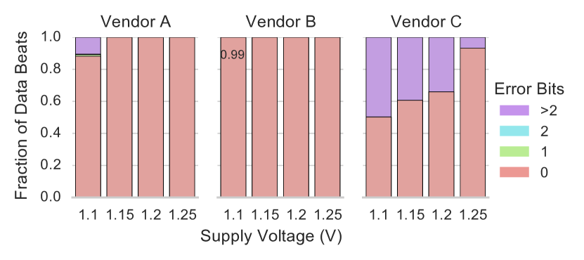
The results show that lowering the supply voltage increases the fraction of beats that contain more than two bits of errors. There are very few beats that contain only one or two error bits. This implies that the most commonly-used ECC scheme, SECDED, is unlikely to alleviate errors induced by a low supply voltage. Another ECC mechanism, Chipkill (sridharan-asplos2015, ; luo-dsn2014, ), protects multiple bit failures within a DRAM chip. However, it cannot correct errors in multiple DRAM chips. Instead, we believe that increasing the access latency, as shown in Section 4.2, is a more effective way of eliminating errors under low supply voltages.
4.5. Effect of Temperature
Temperature is an important external factor that can affect the behavior of DRAM (schroeder-sigmetrics2009, ; el-sayed-sigmetrics2012, ; liu-isca2013, ; khan-sigmetrics2014, ; lee-hpca2015, ; liu-isca2012, ; kim-isca2014, ; lee-thesis2016, ). Prior works have studied the impact of temperature on reliability (schroeder-sigmetrics2009, ; el-sayed-sigmetrics2012, ; kim-isca2014, ; kim-thesis2015, ), latency (lee-hpca2015, ; chang-sigmetrics2016, ; chang-thesis2017, ; lee-thesis2016, ), and retention time (khan-sigmetrics2014, ; liu-isca2013, ; liu-isca2012, ; qureshi-dsn2015, ) at the nominal supply voltage. However, no prior work has studied the effect of temperature on the latency at which DRAM operates reliably, as the supply voltage changes.
To reduce the test time, we test 13 representative DIMMs under a high ambient temperature of 70 using a closed-loop temperature controller (hassan-hpca2017, ). Figure 10 shows the and values of tested DIMMs, categorized by vendor, at 20 and 70. The error bars indicate the minimum and maximum latency values across all DIMMs we tested that are from the same vendor. We increase the horizontal spacing between the low and high temperature data points at each voltage level to improve readability.
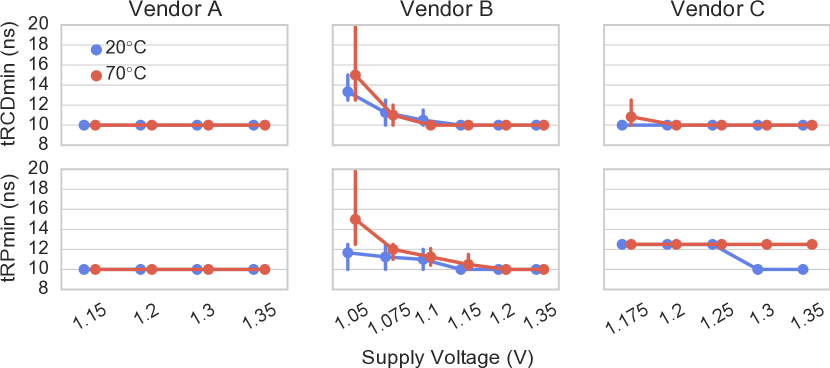
We make two observations. First, temperature impacts vendors differently. On Vendor A’s DIMMs, temperature does not have an observable impact on the reliable operation latencies. Since our platform can test latencies with a step size of only 2.5ns, it is possible that the effect of high temperature on the reliable minimum operating latency for Vendor A’s DIMMs may be within 2.5ns. On the other hand, the temperature effect on latency is measurable on DIMMs from Vendors B and C. DIMMs from Vendor B are not strongly affected by temperature when the supply voltage is above 1.15V. The precharge latency for Vendor C’s DIMMs is affected by high temperature at supply voltages of 1.35V and 1.30V, leading to an increase in the minimum latency from 10ns to 12.5ns. When the voltage is below 1.25V, the impact of high temperature on precharge latency is not observable, as the precharge latency already needs to be raised by 2.5ns, to 12.5ns, at 20. Second, the precharge latency is more sensitive to temperature than the activation latency. Across all of our tested DIMMs, tRP increases with high temperature under a greater number of supply voltage levels, whereas tRCD is less likely to be perturbed by temperature.
Since temperature can affect latency behavior under different voltage levels, techniques that compensate for temperature changes can be used to dynamically adjust the activation and precharge latencies, as proposed by prior work (lee-hpca2015, ; lee-thesis2016, ).
4.6. Impact on Refresh Rate
Recall from Section 2.1 that a DRAM cell uses a capacitor to store data. The charge in the capacitor leaks over time. To prevent data loss, DRAM periodically performs an operation called refresh to restore the charge stored in the cells. The frequency of refresh is determined by the amount of time a cell can retain enough charge without losing information, commonly referred to as a cell’s retention time. For DDR3 DIMMs, the worst-case retention time assumed for a DRAM cell is 64ms (or 32ms at temperatures above 85 (liu-isca2013, ; liu-isca2012, )). Hence, each cell is refreshed every 64ms, which is the DRAM-standard refresh interval.
When we reduce the supply voltage of the DRAM array, we expect the retention time of a cell to decrease, as less charge is stored in each cell. This could potentially require a shorter refresh interval (i.e., more frequent refreshes). To investigate the impact of low supply voltage on retention time, our experiment writes all 1s to every cell, and reads out the data after a given amount of retention time, with refresh disabled. We test a total of seven different retention times (in ms): 64 (the standard time), 128, 256, 512, 1024, 1536, and 2048. We conduct the experiment for ten rounds on every DIMM from all three vendors. Figure 11 shows the average number of weak cells (i.e., cells that experience bit flips due to too much leakage at a given retention time) across all tested DIMMs, for each retention time, under both 20 and 70. We evaluate three voltage levels, 1.35V, 1.2V, and 1.15V, that allow data to be read reliably with a sufficiently long latency. The error bars indicate the 95% confidence interval. We increase the horizontal spacing between the curves at each voltage level to improve readability.
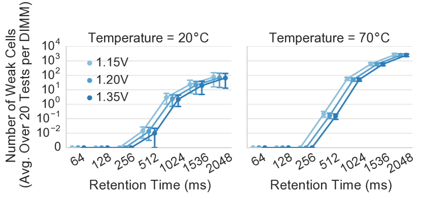
Our results show that every DIMM can retain data for at least 256ms before requiring a refresh operation, which is 4x higher than the standard worst-case specification. These results align with prior works, which also experimentally demonstrate that commodity DRAM cells have much higher retention times than the standard specification of 64ms (kim-edl2009, ; liu-isca2013, ; khan-sigmetrics2014, ; lee-hpca2015, ; hassan-hpca2017, ; lee-thesis2016, ; patel-isca2017, ; qureshi-dsn2015, ). Even though higher retention times (i.e., longer times without refresh) reveal more weak cells, the number of weak cells is still very small, e.g., tens of weak cells out of billions of cells, on average across all DIMMs at under 20. Again, this corresponds closely to observations from prior works showing that there are relatively few weak cells with low retention time in DRAM chips, especially at lower temperatures (kim-edl2009, ; liu-isca2013, ; khan-sigmetrics2014, ; lee-hpca2015, ; hassan-hpca2017, ; qureshi-dsn2015, ; lee-thesis2016, ; patel-isca2017, ).
We observe that the effect of the supply voltage on retention times is not statistically significant. For example, at a 2048ms retention time, the average number of weak cells in a DRAM module increases by only 9 cells (out of a population of billions of cells) when the supply voltage drops from 1.35V (66 weak cells) to 1.15V (75 weak cells) at . For the same 2048ms retention time at , the average number of weak cells increases by only 131 cells when the supply voltage reduces from 1.35V (2510 weak cells) to 1.15V (2641 weak cells).
When we lower the supply voltage, we do not observe any weak cells until a retention time of 512ms, which is 8x the standard refresh interval of 64ms. Therefore, we conclude that using a reduced supply voltage does not require any changes to the standard refresh interval at 20 and 70 ambient temperature.
4.7. Summary
We have presented extensive characterization results and analyses on DRAM chip latency, reliability, and data retention time behavior under various supply voltage levels. We summarize our findings in six key points. First, DRAM reliability worsens (i.e., more errors start appearing) as we reduce the supply voltage below . Second, we discover that voltage-induced errors occur mainly because, at low supply voltages, the DRAM access latency is no longer sufficient to allow the fundamental DRAM operations to complete. Third, via both experiments on real DRAM chips and SPICE simulations, we show that increasing the latency of activation, restoration, and precharge operations in DRAM can mitigate errors under low supply voltage levels until a certain voltage level. Fourth, we show that voltage-induced errors exhibit strong spatial locality in a DRAM chip, clustering at certain locations (i.e., certain banks and rows). Fifth, temperature affects the reliable access latency at low supply voltage levels and the effect is very vendor-dependent. Sixth, we find that reducing the supply voltage does not require increasing the standard DRAM refresh rate for reliable operation below 70.
5. Voltron: Reducing DRAM Energy Without Sacrificing Memory Throughput
Based on the extensive understanding we developed on reduced-voltage operation of real DRAM chips in Section 4, we propose a new mechanism called Voltron, which reduces DRAM energy without sacrificing memory throughput. Voltron exploits the fundamental observation that reducing the supply voltage to DRAM requires increasing the latency of the three DRAM operations in order to prevent errors. Using this observation, the key idea of Voltron is to use a performance model to determine by how much to reduce the DRAM supply voltage, without introducing errors and without exceeding a user-specified threshold for performance loss. Voltron consists of two main components: (i) array voltage scaling, a hardware mechanism that leverages our experimental observations to scale only the voltage supplied to the DRAM array; and (ii) performance-aware voltage control, a software mechanism777Note that this mechanism can also be implemented in hardware, or as a cooperative hardware/software mechanism. that automatically chooses the minimum DRAM array voltage that meets a user-specified performance target.
5.1. Array Voltage Scaling
As we discussed in Section 2.3, the DRAM supply voltage to the peripheral circuitry determines the maximum operating frequency. If we reduce the supply voltage directly, the frequency needs to be lowered as well. As more applications become more sensitive to memory bandwidth, reducing DRAM frequency can result in a substantial performance loss due to lower memory throughput. In particular, we find that reducing the DRAM frequency from 1600 MT/s to 1066 MT/s significantly degrades performance of our evaluated memory-intensive applications by 16.1%. Therefore, the design challenge of Voltron is to reduce the DRAM supply voltage without changing the DRAM frequency.
To address this challenge, the key idea of Voltron’s first component, array voltage scaling, is to reduce the voltage supplied to the DRAM array () without changing the voltage supplied to the peripheral circuitry, thereby allowing the DRAM channel to maintain a high frequency while reducing the power consumption of the DRAM array. To prevent errors from occurring during reduced-voltage operation, Voltron increases the latency of the three DRAM operations (activation, restoration, and precharge) in every DRAM bank based on our observations in Section 4.
By reducing , we effectively reduce (i) the dynamic DRAM power on activate, precharge, and refresh operations; and (ii) the portion of the static power that comes from the DRAM array. These power components decrease quadratically with the square of the array voltage reduction in a modern DRAM chip (keeth-dram-tutorial, ; baker-dram, ). The trade-off is that reducing requires increasing the latency of the three DRAM operations, for reliable operation, thereby leading to some system performance degradation, which we quantify in our evaluation (Section 6).
5.2. Performance-Aware Voltage Control
Array voltage scaling provides system users with the ability to decrease to reduce DRAM power. Employing a lower provides greater power savings, but at the cost of longer DRAM access latency, which leads to larger performance degradation. This trade-off varies widely across different applications, as each application has a different tolerance to the increased memory latency. This raises the question of how to pick a “suitable” array voltage level for different applications as a system user or designer. For this work, we say that an array voltage level is suitable if it does not degrade system performance by more than a user-specified threshold. Our goal is to provide a simple technique that can automatically select a suitable value for different applications. To this end, we propose performance-aware voltage control, a power-performance management policy that selects a minimum that satisfies a desired performance constraint. The key observation is that an application’s performance loss (due to increased memory latency) scales linearly with the application’s memory demand (e.g., memory intensity). Based on this empirical observation we make, we build a performance loss predictor that leverages a linear model to predict an application’s performance loss based on its characteristics at runtime. Using the performance loss predictor, Voltron finds a that can keep the predicted performance within a user-specified target at runtime.
Key Observation. We find that an application’s performance loss due to higher latency has a strong linear relationship with its memory demand (e.g., memory intensity). Figure 12 shows the relationship between the performance loss of each application (due to reduced voltage) and its memory demand under two different reduced-voltage values (see Section 6.1 for our methodology). Each data point represents a single application. Figure 12(a) shows each application’s performance loss versus its memory intensity, expressed using the commonly-used metric MPKI (last-level cache misses per kilo-instruction). Figure 12(b) shows each application’s performance loss versus its memory stall time, the fraction of execution time for which memory requests stall the CPU’s instruction window (i.e., reorder buffer). In Figure 12(a), we see that the performance loss is a piecewise linear function based on the MPKI. The observation that an application’s sensitivity to memory latency is correlated with MPKI has also been made and utilized by prior works (kim-hpca2010, ; kim-micro2010, ; mutlu-isca2008, ; zheng-icpp2008, ; mutlu-micro2007, ; muralidhara-micro2011, ; das-hpca2013, ; das-micro2009, ; usui-taco2016, ; zhao-micro2014, ; das-isca2010, ).
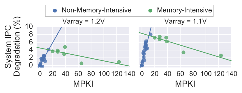

When an application is not memory-intensive (i.e., has an ), its performance loss grows linearly with MPKI, becoming more sensitive to memory latency. Latency-sensitive applications spend most of their time performing computation at the CPU cores and issue memory requests infrequently. As a result, increasing the number of memory requests causes more stall cycles in the CPU.
On the other hand, the performance of memory-intensive applications (i.e., those with ) is less sensitive to memory latency as the MPKI grows. This is because memory-intensive applications experience frequent cache misses and spend a large portion of their time waiting on pending memory requests. As a result, their rate of progress is significantly affected by the memory bandwidth, and therefore they are more sensitive to memory throughput instead of latency. With more outstanding memory requests (i.e., higher MPKI), the memory system is more likely to service them in parallel, leading to more memory-level parallelism (kim-micro2010, ; mutlu-isca2008, ; glew-asploswac98, ; mutlu-hpca2003, ; mutlu-ieeemicro2006, ; lee-micro2009, ). Therefore, improved memory-level parallelism enables applications to tolerate higher latencies more easily.
Figure 12(b) shows that an application’s performance loss increases with its instruction window (reorder buffer) stall time fraction due to memory requests for both memory-intensive and non-memory-intensive applications. A stalled instruction window prevents the CPU from fetching or dispatching new instructions (mutlu-hpca2003, ), thereby degrading the running application’s performance. This observation has also been made and utilized by prior works (ghose-isca2013, ; mutlu-ieeemicro2006, ; mutlu-isca2005, ; mutlu-hpca2003, ).
Performance Loss Predictor. Based on the observed linear relationships between performance loss vs. MPKI and memory stall time fraction, we use ordinary least squares (OLS) regression to develop a piecewise linear model for each application that can serve as the performance loss predictor for Voltron. Equation 1 shows the model, which takes the following inputs: memory latency (), the application’s MPKI, and its memory stall time fraction.
| (1) |
| -30.09 | 0.59 | 0.01 | 19.24 | -50.04 | 1.05 | -0.01 | 15.27 |
|---|
is the predicted performance loss for the application. The subscript refers to each data sample, which describes a particular application’s characteristics (MPKI and memory stall time fraction) and the memory latency associated with the selected voltage level. To generate the data samples, we run a total of 27 workloads across 8 different voltage levels that range from 1.35V to 0.90V, at a 50mV step (see Section 6.1 for our methodology). In total, we generate 216 data samples for finding the coefficients (i.e., and values) in our model. To avoid overfitting the model, we use the scikit-learn machine learning toolkit (scikit, ) to perform cross-validation, which randomly splits the data samples into a training set (151 samples) and a test set (65 samples). To assess the fit of the model, we use a common metric, root-mean-square error (RMSE), which is 2.8 and 2.5 for the low-MPKI and high-MPKI pieces of the model, respectively. Furthermore, we calculate the R2 value to be 0.75 and 0.90 for the low-MPKI and high-MPKI models, respectively. Therefore, the RMSE and R2 metrics indicate that our model provides high accuracy for predicting the performance loss of applications under different values.
Array Voltage Selection. Using the performance loss predictor, Voltron selects the minimum value of that satisfies the given user target for performance loss. Algorithm 1 depicts the array voltage selection component of Voltron. The voltage selection algorithm is executed at periodic intervals throughout the runtime of an application. During each interval, the application’s memory demand is profiled. At the end of an interval, Voltron uses the profile to iteratively compare the performance loss target to the predicted performance loss incurred by each voltage level, starting from a minimum value of 0.90V. Then, Voltron selects the minimum that does not exceed the performance loss target and uses this selected as the DRAM supply voltage in the subsequent interval. In our evaluation, we provide Voltron with a total of 10 voltage levels (every 0.05V step from 0.90V to 1.35V) for selection.
5.3. Implementation
Voltron’s two components require modest modifications to different parts of the system. In order to support array voltage scaling, Voltron requires minor changes to the power delivery network of DIMMs, as commercially-available DIMMs currently use a single supply voltage for both the DRAM array and the peripheral circuitry. Note that this supply voltage goes through separate power pins: and for the DRAM array and peripheral circuitry, respectively, on a modern DRAM chip (micronDDR3L_2Gb, ). Therefore, to enable independent voltage adjustment, we propose to partition the power delivery network on the DIMM into two domains: one domain to supply only the DRAM array () and the other domain to supply only the peripheral circuitry ().
Performance-aware voltage control requires (i) performance monitoring hardware that records the MPKI and memory stall time of each application; and (ii) a control algorithm block, which predicts the performance loss at different values and accordingly selects the smallest acceptable . Voltron utilizes the performance counters that exist in most modern CPUs to perform performance monitoring, thus requiring no additional hardware overhead. Voltron reads these counter values and feeds them into the array voltage selection algorithm, which is implemented in the system software layer. Although reading the performance monitors has a small amount of software overhead, we believe the overhead is negligible because we do so only at the end of each interval (i.e., every four million cycles in most of our evaluations; see sensitivity studies in Section 6.8).
Voltron periodically executes this performance-aware voltage control mechanism during the runtime of the target application. During each time interval, Voltron monitors the application’s behavior through hardware counters. At the end of an interval, the system software executes the array voltage selection algorithm to select the predicted and accordingly adjust the timing parameters stored in the memory controller for activation, restoration, and precharge. Note that there could be other (e.g., completely hardware-based) implementations of Voltron. We leave a detailed explanation of different implementations to future work.
6. System Evaluation
In this section, we evaluate the system-level performance and energy impact of Voltron. We present our evaluation methodology in Section 6.1. Next, we study the energy savings and performance loss when we use array voltage scaling without any control (Section 6.2). We study how performance-aware voltage control delivers overall system energy reduction with only a modest amount of performance loss (Sections 6.3 and 6.4). We then evaluate an enhanced version of Voltron , which exploits spatial error locality (Section 6.5). Finally, Sections 6.6 to 6.8 present sensitivity studies of Voltron to various system and algorithm parameters.
6.1. Methodology
We evaluate Voltron using Ramulator (kim-cal2015, ), a detailed and and cycle-accurate open-source DRAM simulator (ram-github, ), integrated with a multi-core performance simulator. We model a low-power mobile system that consists of 4 ARM cores and DDR3L DRAM. Table 2 shows our system parameters. Such a system resembles existing commodity devices, such as the Google Chromebook (chromebook, ) or the NVIDIA SHIELD tablet (shield, ). To model the energy consumption, we use McPAT (mcpat:micro, ) for the processor and DRAMPower (drampower, ) for the DRAM-based memory system. We open-source the code of Voltron (volt-github, ).
| Processor | 4 ARM Cortex-A9 cores (arma9, ), 2GHz, |
|---|---|
| 192-entry instruction window | |
| Cache | L1: 64KB/core, L2: 512KB/core, L3: 2MB shared |
| Memory | 64/64-entry read/write request queue, FR-FCFS (rixner-isca2000, ; zuravleff-patent, ) |
| Controller | |
| DRAM | DDR3L-1600 (jedec-ddr3l, ) |
| 2 channels (1 rank and 8 banks per channel) |
Table 3 lists the latency values we evaluate for each DRAM array voltage (). The latency values are obtained from our SPICE model using data from real devices (Section 4.2), which is available online (volt-github, ).888In this work, we do not have experimental data on the restoration latency (tRAS) under reduced-voltage operation. This is because our reduced-voltage tests access cache lines sequentially from each DRAM row, and tRAS overlaps with the latency of reading all of the cache lines from the row. Instead of designing a separate test to measure tRAS, we use our circuit simulation model (Section 4.2) to derive tRAS values for reliable operation under different voltage levels. We leave the thorough experimental evaluation of tRAS under reduced-voltage operation to future work. To account for manufacturing process variation, we conservatively add in the same latency guardband (i.e., 38%) used by manufacturers at the nominal voltage level of 1.35V to each of our latency values. We then round up each latency value to the nearest clock cycle time (i.e., 1.25ns).
| tRCD - tRP - tRAS (ns) | tRCD - tRP - tRAS (ns) | ||
|---|---|---|---|
| 1.35 | 13.75 - 13.75 - 36.25 | 1.10 | 15.00 - 16.25 - 40.00 |
| 1.30 | 13.75 - 13.75 - 36.25 | 1.05 | 16.25 - 17.50 - 41.25 |
| 1.25 | 13.75 - 15.00 - 36.25 | 1.00 | 17.50 - 18.75 - 45.00 |
| 1.20 | 13.75 - 15.00 - 37.50 | 0.95 | 18.75 - 21.25 - 48.75 |
| 1.15 | 15.00 - 15.00 - 37.50 | 0.90 | 21.25 - 26.25 - 52.50 |
Workloads. We evaluate 27 benchmarks from SPEC CPU2006 (spec2006, ) and YCSB (cooper-socc2010, ), as shown in Table 4 along with each benchmark’s L3 cache MPKI, i.e., memory intensity. We use the 27 benchmarks to form homogeneous and heterogeneous multiprogrammed workloads. For each homogeneous workload, we replicate one of our benchmarks by running one copy on each core to form a four-core multiprogrammed workload, as done in many past works that evaluate multi-core system performance (lee-hpca2015, ; chang-sigmetrics2016, ; lee-hpca2013, ; nair-isca2013, ; nair-micro2014, ; shafiee-hpca2014, ; shevgoor-micro2013, ; chatterjee-micro2012, ). Evaluating homogeneous workloads enables easier analysis and understanding of the system. For each heterogeneous workload, we combine four different benchmarks to create a four-core workload. We categorize the heterogeneous workloads by varying the fraction of memory-intensive benchmarks in each workload (0%, 25%, 50%, 75%, and 100%). Each category consists of 10 workloads, resulting in a total of 50 workloads across all categories. Our simulation executes at least 500 million instructions on each core. We calculate system energy as the product of the average dissipated power (from both CPU and DRAM) and the workload runtime. We measure system performance with the commonly-used weighted speedup (WS) metric (snavely-asplos2000, ), which is a measure of job throughput on a multi-core system (eyerman-ieeemicro2008, ).
| Number | Name | L3 MPKI | Number | Name | L3 MPKI | |
|---|---|---|---|---|---|---|
| 0 | YCSB-a | 6.66 | 14 | h264ref | 2.14 | |
| 1 | YCSB-b | 5.95 | 15 | hmmer | 6.33 | |
| 2 | YCSB-c | 5.74 | 16 | libquantum | 37.95 | |
| 3 | YCSB-d | 5.30 | 17 | mcf | 123.65 | |
| 4 | YCSB-e | 6.07 | 18 | milc | 27.91 | |
| 5 | astar | 3.43 | 19 | namd | 2.76 | |
| 6 | bwaves | 19.97 | 20 | omnetpp | 27.87 | |
| 7 | bzip2 | 8.23 | 21 | perlbench | 0.95 | |
| 8 | cactusADM | 6.79 | 22 | povray | 0.01 | |
| 9 | calculix | 0.01 | 23 | sjeng | 0.73 | |
| 10 | gamess | 0.01 | 24 | soplex | 64.98 | |
| 11 | gcc | 3.20 | 25 | sphinx3 | 13.59 | |
| 12 | GemsFDTD | 39.17 | 26 | zeusmp | 4.88 | |
| 13 | gobmk | 3.94 |
6.2. Impact of Array Voltage Scaling
In this section, we evaluate how array voltage scaling (Section 5.1) affects the system energy consumption and application performance of our homogeneous workloads at different values. We split our discussion into two parts: the results for memory-intensive workloads (i.e., applications where MPKI 15 for each core), and the results for non-memory-intensive workloads.
Memory-Intensive Workloads. Figure 13 shows the system performance (WS) loss, DRAM power reduction, and system energy reduction, compared to a baseline DRAM with 1.35V, when we vary from 1.30V to 0.90V. We make three observations from these results.


First, system performance loss increases as we lower , due to the increased DRAM access latency. However, different workloads experience a different rate of performance loss, as they tolerate memory latency differently. Among the memory-intensive workloads, mcf exhibits the lowest performance degradation since it has the highest memory intensity and high memory-level parallelism, leading to high queuing delays in the memory controller. The queuing delays and memory-level parallelism hide the longer DRAM access latency more than in other workloads. Other workloads lose more performance because they are less able to tolerate/hide the increased latency. Therefore, workloads with very high memory intensity and memory-level parallelism can be less sensitive to the increased memory latency.
Second, DRAM power savings increase with lower since reducing the DRAM array voltage decreases both the dynamic and static power components of DRAM. However, system energy savings does not monotonically increase with lower . We find that using =0.9V provides lower system energy savings than using =1.0V, as the processor takes much longer to run the applications at =0.9V. In this case, the increase in static DRAM and CPU energy outweighs the dynamic DRAM energy savings.
Third, reducing leads to a system energy reduction only when the reduction in DRAM energy outweighs the increase in CPU energy (due to the longer execution time). For =1.1V, the system energy reduces by an average of 7.6%. Therefore, we conclude that array voltage scaling is an effective technique that improves system energy consumption, with a small performance loss, for memory-intensive workloads.
Non-Memory-Intensive Workloads. Table 5 summarizes the system performance loss and energy savings of 20 non-memory-intensive workloads as varies from 1.30V to 0.90V, over the performance and energy consumption under a nominal of 1.35V. Compared to the memory-intensive workloads, non-memory-intensive workloads obtain smaller system energy savings, as the system energy is dominated by the processor. Although the workloads are more compute-intensive, lowering does reduce their system energy consumption, by decreasing the energy consumption of DRAM. For example, at 1.2V, array voltage scaling achieves an overall system energy savings of 2.5% with a performance loss of only 1.4%.
| 1.3V | 1.2V | 1.1V | 1.0V | 0.9V | |
|---|---|---|---|---|---|
| System Performance Loss (%) | 0.5 | 1.4 | 3.5 | 7.1 | 14.2 |
| DRAM Power Savings (%) | 3.4 | 10.4 | 16.5 | 22.7 | 29.0 |
| System Energy Savings (%) | 0.8 | 2.5 | 3.5 | 4.0 | 2.9 |
6.3. Effect of Performance-Aware Voltage Control
In this section, we evaluate the effectiveness of our complete proposal for Voltron, which incorporates our performance-aware voltage control mechanism to drive the array voltage scaling component intelligently. The performance-aware voltage control mechanism selects the lowest voltage level that satisfies the performance loss bound (provided by the user or system designer) based on our performance model (see Section 5.2). We evaluate Voltron with a target performance loss of 5%. Voltron executes the performance-aware voltage control mechanism once every four million cycles.999We evaluate the sensitivity to the frequency at which we execute the mechanism (i.e., the interval length of Voltron) in Section 6.8. We quantitatively compare Voltron to MemDVFS, a dynamic DRAM frequency and voltage scaling mechanism proposed by prior work (david-icac2011, ), which we describe in Section 2.4. Similar to the configuration used in the prior work, we enable MemDVFS to switch dynamically between three frequency steps: 1600, 1333, and 1066 MT/s, which employ supply voltages of 1.35V, 1.3V, and 1.25V, respectively.
Figure 14 shows the system performance (WS) loss, DRAM power savings, and system energy savings due to MemDVFS and Voltron, compared to a baseline DRAM with a supply voltage of 1.35V. We show one graph per metric, where each graph uses boxplots to show the distribution among all workloads. In each graph, we categorize the workloads as either non-memory-intensive or memory-intensive. Each box illustrates the quartiles of the population, and the whiskers indicate the minimum and maximum values. The red dot indicates the mean. We make four major observations.
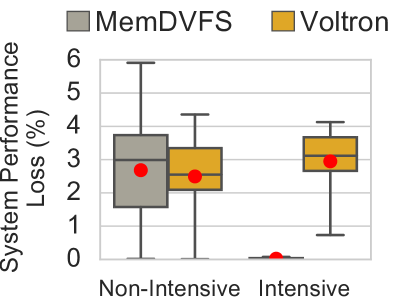
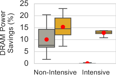
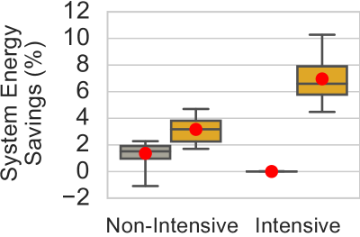
First, as shown in Figure 14(a), Voltron consistently selects a value that satisfies the performance loss bound of 5% across all workloads. Voltron incurs an average (maximum) performance loss of 2.5% (4.4%) and 2.9% (4.1%) for non-memory-intensive and memory-intensive workloads, respectively. This demonstrates that our performance model enables Voltron to select a low voltage value that saves energy while bounding performance loss based on the user’s requirement. We evaluate Voltron with a range of different performance targets in Section 6.7.
Second, MemDVFS has almost zero effect on memory-intensive workloads. This is because MemDVFS avoids scaling DRAM frequency (and hence voltage) when an application’s memory bandwidth utilization is above a fixed threshold. Reducing the frequency can result in a large performance loss since the memory-intensive workloads require high memory throughput. As memory-intensive applications have high memory bandwidth consumption that easily exceeds the fixed threshold used by MemDVFS, MemDVFS cannot perform frequency and voltage scaling during most of the execution time. These results are consistent with the results reported in MemDVFS (david-icac2011, ). In contrast, Voltron reduces system energy (shown in Figure 14(c)) by 7.0% on average for memory-intensive workloads, at the cost of 2.9% system performance loss, which is well within the specified performance loss target of 5% (shown in Figure 14(a)).
Third, both MemDVFS and Voltron reduce the average system energy consumption for non-memory-intensive workloads. MemDVFS reduces system energy by dynamically scaling the frequency and voltage of DRAM, which lowers the DRAM power consumption (as shown in Figure 14(b)). By reducing the DRAM array voltage to a lower value than MemDVFS, Voltron is able to provide a slightly higher DRAM power and system energy reduction for non-memory-intensive workloads than MemDVFS.
Fourth, although Voltron reduces the system energy with a small performance loss, the average system energy efficiency, in terms of performance per watt (not shown in the figure), still improves by 3.3% and 7.4% for non-memory-intensive and memory-intensive workloads, respectively, over the baseline. Thus, we demonstrate that Voltron is an effective mechanism that improves system energy efficiency not only on non-memory-intensive applications, but also (especially) on memory-intensive workloads where prior work was unable to do so.
To summarize, across non-memory-intensive and memory-intensive workloads, Voltron reduces the average system energy consumption by 3.2% and 7.0% while limiting average system performance loss to only 2.5% and 2.9%, respectively. Voltron ensures that no workload loses performance by more than the specified target of 5%. We conclude that Voltron is an effective DRAM and system energy reduction mechanism that significantly outperforms prior memory DVFS mechanisms.
6.4. System Energy Breakdown
To demonstrate the source of energy savings from Voltron, Figure 15 compares the system energy breakdown of Voltron to the baseline, which operates at the nominal voltage level of 1.35V. The breakdown shows the average CPU and DRAM energy consumption across workloads, which are categorized into non-memory-intensive and memory-intensive workloads. We make two observations from the figure.
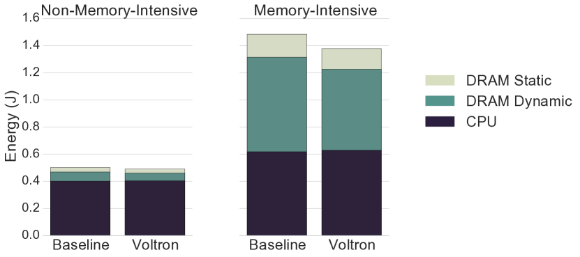
First, in the non-memory-intensive workloads, the CPU consumes an average of 80% of the total system energy when the DRAM uses the nominal voltage level. As a result, Voltron has less potential to reduce the overall system energy as it reduces only the DRAM energy, which makes up only 20% of the total system energy. Second, DRAM consumes an average of 53% of the total system energy in the memory-intensive workloads. As a result, Voltron has a larger room for potential improvement for memory-intensive workloads than for non-memory-intensive workloads. Across the memory-intensive workloads, Voltron reduces the average dynamic and static DRAM energy by 14% and 11%, respectively. However, Voltron increases the CPU energy consumption by 1.7%, because the application incurs a small system performance degradation (due to the increased memory access latency), which is within our 5% performance loss target (as shown in Section 6.3). We conclude that Voltron is effective in reducing DRAM energy, and it is an effective system energy reduction mechanism, especially when DRAM is a major consumer of energy in the system.
6.5. Effect of Exploiting Spatial Locality of Errors
In Section 4.3, our experimental results show that errors due to reduced voltage concentrate in certain regions, specifically in select DRAM banks for some vendors’ DIMMs. This implies that when we lower the voltage, only the banks with errors require a higher access latency to read or write data correctly, whereas error-free banks can be accessed reliably with the standard latency. Therefore, in this section, we enhance our Voltron mechanism by exploiting the spatial locality of errors caused by reduced-voltage operations. The key idea is to dynamically change the access latency on a per-bank basis (i.e., based on the DRAM banks being accessed) to account for the reliability of each bank. In other words, we would like to increase the latency only for banks that would otherwise experience errors, and do so just enough such that these banks operate reliably.
For our evaluation, we model the behavior based on a subset (three) of Vendor C’s DIMMs, which show that the number of banks with errors increases as we reduce the supply voltage (Section 4.3). We observe that these DIMMs start experiencing errors at 1.1V using the standard latency values. However, only one bank observes errors when we reduce the voltage level from 1.15V to 1.1V (i.e., 50mV reduction). We evaluate a conservative model that increases the number of banks that need higher latency by one for every 50mV reduction from the nominal voltage of 1.35V. Note that this model is conservative, because we start increasing the latency when the voltage is reduced to 1.3V, which is much higher than the lowest voltage level (1.15V) for which we observe that DIMMs operate reliably without requiring a latency increase. Based on this conservative model, we choose the banks whose latencies should increase sequentially starting from the first bank, while the remaining banks operate at the standard latency. For example, at 1.25V (100mV lower than the nominal voltage of 1.35V), Voltron needs to increase the latency for the first two out of the eight banks to ensure reliable operation.
Figure 16(a) compares the system performance and energy efficiency of our bank-error locality aware version of Voltron (denoted as Voltron+BL) to the previously-evaluated Voltron mechanism, which is not aware of such locality. By increasing the memory latency for only a subset of banks at each voltage step, Voltron+BL reduces the average performance loss from 2.9% to 1.8% and increases the average system energy savings from 7.0% to 7.3% for memory-intensive workloads, with similar improvements for non-memory-intensive workloads. We show that enhancing Voltron by adding awareness of the spatial locality of errors can further mitigate the latency penalty due to reduced voltage, even with the conservative bank error locality model we assume and evaluate in this example. We believe that a mechanism that exploits spatial error locality at a finer granularity could lead to even higher performance and energy savings, but we leave such an evaluation to future work.
[0.49]
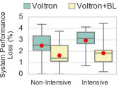 [0.49]
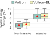
6.6. Effect on Heterogeneous Workloads
[0.49]
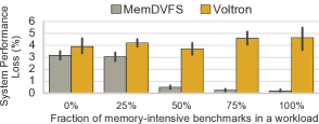 [0.49]
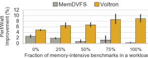
So far, we have evaluated Voltron on homogeneous multi-core workloads, where each workload consists of the same benchmark running on all cores. In this section, we evaluate the effect of Voltron on heterogeneous workloads, where each workload consists of different benchmarks running on each core. We categorize the workloads based on the fraction of memory-intensive benchmarks in the workload (0%, 25%, 50%, 75%, and 100%). Each category consists of 10 workloads, resulting in a total of 50 workloads across all categories.
Figure 17 shows the system performance loss and energy efficiency improvement (in terms of performance per watt) with Voltron and with MemDVFS for heterogeneous workloads. The error bars indicate the 95% confidence intervals across all workloads in the category. We make two observations from the figure. First, for each category of the heterogeneous workloads, Voltron is able to meet the 5% performance loss target on average. However, since Voltron is not designed to provide a hard performance guarantee for every single workload, Voltron exceeds the performance loss target for 10 out of the 50 workloads, though it exceeds the target by only 0.76% on average. Second, the energy efficiency improvement due to Voltron becomes larger as the memory intensity of the workload increases. This is because the fraction of system energy coming from memory grows with higher memory intensity, due to the higher amount of memory traffic. Therefore, the memory energy reduction from Voltron has a greater impact at the system level with more memory-intensive workloads. On the other hand, MemDVFS becomes less effective with higher memory intensity, as the memory bandwidth utilization more frequently exceeds the fixed threshold employed by MemDVFS. Thus, MemDVFS has a smaller opportunity to scale the frequency and voltage. We conclude that Voltron is an effective mechanism that can adapt to different applications’ characteristics to improve system energy efficiency.
6.7. Effect of Varying the Performance Target
Figure 18(a) shows the performance loss and energy efficiency improvement due to Voltron as we vary the system performance loss target for both homogeneous and heterogeneous workloads. For each target, we use a boxplot to show the distribution across all workloads. In total, we evaluate Voltron on 1001 combinations of workloads and performance targets: 27 homogeneous workloads 13 targets + 50 heterogeneous workloads 13 targets. The first major observation is that Voltron’s performance-aware voltage control mechanism adapts to different performance targets by dynamically selecting different voltage values at runtime. Across all 1001 runs, Voltron keeps performance within the performance loss target for 84.5% of them. Even though Voltron cannot enforce a hard performance guarantee for all workloads, it exceeds the target by only 0.68% on average for those workloads where it does not strictly meet the target.
[][c]
 [][c]
[][c]
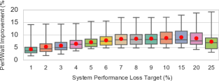
Second, system energy efficiency increases with higher performance loss targets, but the gains plateau at around a target of 10%. Beyond the 10% target, Voltron starts selecting smaller values (e.g., 0.9V) that result in much higher memory latency, which in turn increases both the CPU runtime and system energy. In Section 6.2, we observed that employing a value less than 1.0V can result in smaller system energy savings than using =1.0V.
We conclude that, compared to prior work on memory DVFS, Voltron is a more flexible mechanism, as it allows the users or system designers to select a performance and energy trade-off that best suits their target system or applications.
6.8. Sensitivity to the Profile Interval Length
Figure 19 shows the average system energy efficiency improvement due to Voltron with different profile interval lengths measured across 27 homogeneous workloads. As the profile interval length increases beyond two million cycles, we observe that the energy efficiency benefit of Voltron starts reducing. This is because longer intervals prevent Voltron from making faster adjustments based on the collected new profile information. Nonetheless, Voltron consistently improves system energy efficiency for all evaluated profile interval lengths.

7. Related Work
To our knowledge, this is the first work to (i) experimentally characterize the reliability and performance of modern low-power DRAM chips under different supply voltages, and (ii) introduce a new mechanism that reduces DRAM energy while retaining high memory data throughput by adjusting the DRAM array voltage. We briefly discuss other prior work in DRAM energy reduction.
DRAM Frequency and Voltage Scaling. We have already discussed the most relevant works on DRAM frequency and voltage scaling, and provided qualitative comparisons in Section 2.4. None of these works provide a comprehensive experimental analysis of the impact of using a wide range of supply voltages on DRAM reliability, latency, and refresh. In contrast to all these works, our work focuses on a detailed experimental characterization of real DRAM chips as the supply voltage varies. Our study provides fundamental observations for potential mechanisms that can mitigate DRAM and system energy consumption. Furthermore, frequency scaling hurts memory throughput, and thus significantly degrades the system performance of especially memory-intensive workloads (see Section 5.1 for our quantitative comparison). We demonstrate the importance and benefits of exploiting our experimental observations by proposing Voltron, one new example mechanism that uses our observations to reduce DRAM and system energy without sacrificing memory throughput.
Low-Power Modes for DRAM. Modern DRAM chips support various low-power standby modes. Entering and exiting these modes incurs some amount of latency, which delays memory requests that must be serviced. To increase the opportunities to exploit these low-power modes, several prior works propose mechanisms that increase periods of memory idleness through data placement (e.g., (lebeck-asplos2000, ; fan-islped2001, )) and memory traffic reshaping (e.g., (aggarwal-hpca2008, ; bi-hpca2010, ; amin-islped2010, ; lyuh-dac2004, ; diniz-isca2007, )). Exploiting low-power modes is orthogonal to our work on studying the impact of reduced-voltage operation in DRAM. Furthermore, low-power modes have a smaller effect on memory-intensive workloads, which exhibit little idleness in memory accesses, whereas, as we showed in Section 6.3, our mechanism is especially effective on memory-intensive workloads.
Low-Power DDR DRAM Chips. Low-power DDR (LPDDR) (jedec-lpddr3, ; jedec-lpddr4, ) is a specific type of DRAM that is optimized for low-power systems like mobile devices. To reduce power consumption, LPDDRx (currently in its 4th generation) employs a few major design changes that differ from conventional DDRx chips. First, LPDDRx uses a low-voltage swing I/O interface that consumes 40% less I/O power than DDR4 DRAM (choi-memcon2013, ). Second, it supports additional low-power modes with a lower supply voltage. Since the LPDDRx array design remains the same as DDRx, our observations on the correlation between access latency and array voltage are applicable to LPDDRx DRAM as well. Our proposed Voltron approach can provide significant benefits in LPDDRx, since array energy consumption is significantly higher than the energy consumption of peripheral circuitry in LPDDRx chips (choi-memcon2013, ). We leave the detailed evaluation of LPDDRx chips for future work since our current experimental platform is not capable of evaluating them.
Low-Power DRAM Architectures. Prior works (e.g., (udipi-isca2010, ; zhang-isca2014, ; cooper-balis-ieeemicro2010, ; chatterjee-hpca2017, )) propose to modify the DRAM chip architecture to reduce the ACTIVATE power by activating only a fraction of a row instead of the entire row. Another common technique, called sub-ranking, reduces dynamic DRAM power by accessing data from a subset of chips from a DRAM module (zheng-micro2008, ; yoon-isca2011, ; ware-iccd2006, ). A couple of prior works (malladi-isca2012, ; yoon-isca2012, ) propose DRAM module architectures that integrate many low-frequency LPDDR chips to enable DRAM power reduction. These proposed changes to DRAM chips or DIMMs are orthogonal to our work.
Reducing Refresh Power. In modern DRAM chips, although different DRAM cells have widely different retention times (liu-isca2013, ; kim-edl2009, ), memory controllers conservatively refresh all of the cells based on the retention time of a small fraction of weak cells, which have the longest retention time out of all of the cells. To reduce DRAM refresh power, many prior works (e.g., (liu-isca2012, ; agrawal-hpca2014, ; qureshi-dsn2015, ; liu-isca2013, ; venkatesan-hpca2006, ; bhati-isca2015, ; lin-iccd2012, ; ohsawa-islped1998, ; patel-isca2017, ; khan-sigmetrics2014, ; khan-dsn2016, ; khan2016case, )) propose mechanisms to reduce unnecessary refresh operations, and, thus, refresh power, by characterizing the retention time profile (i.e., the data retention behavior of each cell) within the DRAM chips. However, these techniques do not reduce the power of other DRAM operations, and these prior works do not provide an experimental characterization of the effect of reduced voltage levels on data retention time.
Improving DRAM Energy Efficiency by Reducing Latency or Improving Parallelism. Various prior works (e.g., (hassan-hpca2016, ; lee-hpca2015, ; chang-hpca2014, ; lee-thesis2016, ; lee-hpca2013, ; lee-sigmetrics2017, ; lee-arxiv2016, ; kim-isca2012, ; lee-thesis2016, ; lee-taco2016, ; seshadri-micro2013, ; chang2016low, ; lee-pact2015, )) improve DRAM energy efficiency by reducing the execution time through techniques that reduce the DRAM access latency or improve parallelism between memory requests. These mechanisms are orthogonal to ours, because they do not reduce the voltage level of DRAM.
Experimental Studies of DRAM Chips. Recent works experimentally investigate various reliability, data retention, and latency characteristics of modern DRAM chips (liu-isca2012, ; liu-isca2013, ; kim-isca2014, ; chang-sigmetrics2016, ; lee-hpca2015, ; lee-sigmetrics2017, ; chandrasekar-date2014, ; khan-sigmetrics2014, ; jung-memsys2016, ; jung-patmos2016, ; hassan-hpca2017, ; khan-dsn2016, ; patel-isca2017, ; lee-arxiv2016, ; lee-thesis2016, ; kim-thesis2015, ; meza2015revisiting, ; schroeder-sigmetrics2009, ; sridharan-asplos2015, ; sridharan2012study, ). None of these works study these characteristics under reduced-voltage operation, which we do in this paper.
Reduced-Voltage Operation in SRAM Caches. Prior works propose different techniques to enable SRAM caches to operate under reduced voltage levels (e.g., (alameldeen-isca2011, ; alameldeen-tc2011, ; wilkerson-ieeemicro2009, ; chishti-micro2009, ; roberts-dsd2007, ; wilkerson-isca2008, )). These works are orthogonal to our experimental study because we focus on understanding and enabling reduced-voltage operation in DRAM, which is a significantly different memory technology than SRAM.
8. Conclusion
This paper provides the first experimental study that comprehensively characterizes and analyzes the behavior of DRAM chips when the supply voltage is reduced below its nominal value. We demonstrate, using 124 DDR3L DRAM chips, that the DRAM supply voltage can be reliably reduced to a certain level, beyond which errors arise within the data. We then experimentally demonstrate the relationship between the supply voltage and the latency of the fundamental DRAM operations (activation, restoration, and precharge). We show that bit errors caused by reduced-voltage operation can be eliminated by increasing the latency of the three fundamental DRAM operations. By changing the memory controller configuration to allow for the longer latency of these operations, we can thus further lower the supply voltage without inducing errors in the data. We also experimentally characterize the relationship between reduced supply voltage and error locations, stored data patterns, temperature, and data retention.
Based on these observations, we propose and evaluate Voltron, a low-cost energy reduction mechanism that reduces DRAM energy without affecting memory data throughput. Voltron reduces the supply voltage for only the DRAM array, while maintaining the nominal voltage for the peripheral circuitry to continue operating the memory channel at a high frequency. Voltron uses a new piecewise linear performance model to find the array supply voltage that maximizes the system energy reduction within a given performance loss target. Our experimental evaluations across a wide variety of workloads demonstrate that Voltron significantly reduces system energy consumption with only very modest performance loss.
We conclude that it is very promising to understand and exploit reduced-voltage operation in modern DRAM chips. We hope that the experimental characterization, analysis, and optimization techniques presented in this paper will enable the development of other new mechanisms that can effectively exploit the trade-offs between voltage, reliability, and latency in DRAM to improve system performance, efficiency, and/or reliability.
Acknowledgements.
We thank our shepherd Benny Van Houdt, the anonymous reviewers of SIGMETRICS 2017, and the SAFARI group members for feedback. We acknowledge the support of Google, Intel, NVIDIA, Samsung, VMware, and the United States Department of Energy. This research was supported in part by the ISTC-CC, SRC, and NSF (grants 1212962 and 1320531). Kevin Chang is supported in part by an SRCEA/Intel Fellowship.References
- (1) “Predictive Technology Model,” 2007.
- (2) “Ramulator,” https://github.com/CMU-SAFARI/ramulator, 2015.
- (3) “DRAM Voltage Study,” https://github.com/CMU-SAFARI/DRAM-Voltage-Study, 2017.
- (4) Advanced Micro Devices, Inc., “AMD Opteron 4300 Series Processors,” http://www.amd.com/en-us/products/server/4000/4300.
- (5) Advanced Micro Devices, Inc., “BKDG for AMD Family 16h Models 00h-0Fh Processors,” Oct. 2013.
- (6) N. Aggarwal, J. F. Cantin, M. H. Lipasti, and J. E. Smith, “Power-Efficient DRAM Speculation,” in HPCA, 2008.
- (7) A. Agrawal, A. Ansari, and J. Torrellas, “Mosaic: Exploiting the Spatial Locality of Process Variation to Reduce Refresh Energy in On-Chip eDRAM Modules,” in HPCA, 2014.
- (8) A. R. Alameldeen, Z. Chishti, C. Wilkerson, W. Wu, and S.-L. Lu, “Adaptive Cache Design to Enable Reliable Low-Voltage Operation,” IEEE TC, 2011.
- (9) A. R. Alameldeen, I. Wagner, Z. Chishti, W. Wu, C. Wilkerson, and S.-L. Lu, “Energy-Efficient Cache Design Using Variable-Strength Error-Correcting Codes,” in ISCA, 2011.
- (10) A. M. Amin and Z. A. Chishti, “Rank-Aware Cache Replacement and Write Buffering to Improve DRAM Energy Efficiency,” in ISLPED, 2010.
- (11) ARM Ltd., “Cortex-A9 Processor,” https://www.arm.com/products/processors/cortex-a/cortex-a9.php.
- (12) R. J. Baker, CMOS Circuit Design, Layout, and Simulation. Wiley-IEEE Press, 2010.
- (13) H. Bauer, S. Burghardt, S. Tandon, and F. Thalmayr, “Memory: Are Challenges Ahead?” March 2016. http://www.mckinsey.com/industries/semiconductors/our-insights/memory-are-challenges-ahead
- (14) R. Begum, D. Werner, M. Hempstead, G. Prasad, and G. Challen, “Energy-Performance Trade-Offs on Energy-Constrained Devices with Multi-component DVFS,” in IISWC, 2015.
- (15) I. Bhati, Z. Chishti, S.-L. Lu, and B. Jacob, “Flexible Auto-Refresh: Enabling Scalable and Energy-Efficient DRAM Refresh Reductions,” in ISCA, 2015.
- (16) M. Bi, R. Duan, and C. Gniady, “Delay-Hiding Energy Management Mechanisms for DRAM,” in HPCA, 2010.
- (17) K. Chandrasekar, S. Goossens, C. Weis, M. Koedam, B. Akesson, N. Wehn, and K. Goossens, “Exploiting Expendable Process-Margins in DRAMs for Run-Time Performance Optimization,” in DATE, 2014.
- (18) K. Chandrasekar, C. Weis, Y. Li, S. Goossens, M. Jung, O. Naji, B. Akesson, N. Wehn, and K. Goossens, “DRAMPower: Open-Source DRAM Power & Energy Estimation Tool,” http://www.drampower.info.
- (19) K. K. Chang, D. Lee, Z. Chishti, A. Alameldeen, C. Wilkerson, Y. Kim, and O. Mutlu, “Improving DRAM Performance by Parallelizing Refreshes with Accesses,” in HPCA, 2014.
- (20) K. K. Chang, “Understanding and Improving the Latency of DRAM-Based Memory Systems,” Ph.D. dissertation, Carnegie Mellon University, 2017.
- (21) K. K. Chang, A. Kashyap, H. Hassan, S. Ghose, K. Hsieh, D. Lee, T. Li, G. Pekhimenko, S. Khan, and O. Mutlu, “Understanding Latency Variation in Modern DRAM Chips: Experimental Characterization, Analysis, and Optimization,” in SIGMETRICS, 2016.
- (22) K. K. Chang, P. J. Nair, D. Lee, S. Ghose, M. K. Qureshi, and O. Mutlu, “Low-Cost Inter-Linked Subarrays (LISA): Enabling Fast Inter-Subarray Data Movement in DRAM,” in HPCA, 2016.
- (23) N. Chatterjee, M. Shevgoor, R. Balasubramonian, A. Davis, Z. Fang, R. Illikkal, and R. Iyer, “Leveraging Heterogeneity in DRAM Main Memories to Accelerate Critical Word Access,” in MICRO, 2012.
- (24) N. Chatterjee, M. O’Connor, D. Lee, D. R. Johnson, M. Rhu, S. W. Kecker, and W. J. Dally, “Architecting an Energy-Efficient DRAM System for GPUs,” in HPCA, 2017.
- (25) Z. Chishti, A. R. Alameldeen, C. Wilkerson, W. Wu, and S.-L. Lu, “Improving Cache Lifetime Reliability at Ultra-Low Voltages,” in MICRO, 2009.
- (26) J. Y. Choi, “LPDDR4: Evolution for New Mobile World,” in MEMCON, 2013.
- (27) B. F. Cooper, A. Silberstein, E. Tam, R. Ramakrishnan, and R. Sears, “Benchmarking Cloud Serving Systems with YCSB,” in SOCC, 2010.
- (28) E. Cooper-Balis and B. Jacob, “Fine-Grained Activation for Power Reduction in DRAM,” IEEE Micro, 2010.
- (29) R. Das, R. Ausavarungnirun, O. Mutlu, A. Kumar, and M. Azimi, “Application-to-Core Mapping Policies to Reduce Memory System Interference in Multi-Core Systems,” in HPCA, 2013.
- (30) R. Das, O. Mutlu, T. Moscibroda, and C. Das, “Application-Aware Prioritization Mechanisms for On-Chip Networks,” in MICRO, 2009.
- (31) R. Das, O. Mutlu, T. Moscibroda, and C. R. Das, “Aérgia: Exploiting Packet Latency Slack in On-Chip Networks,” in ISCA, 2010.
- (32) H. David, C. Fallin, E. Gorbatov, U. R. Hanebutte, and O. Mutlu, “Memory Power Management via Dynamic Voltage/Frequency Scaling,” in ICAC, 2011.
- (33) Q. Deng, D. Meisner, A. Bhattacharjee, T. F. Wenisch, and R. Bianchini, “CoScale: Coordinating CPU and Memory System DVFS in Server Systems,” in MICRO, 2012.
- (34) Q. Deng, D. Meisner, A. Bhattacharjee, T. F. Wenisch, and R. Bianchini, “MultiScale: Memory System DVFS with Multiple Memory Controllers,” in ISLPED, 2012.
- (35) Q. Deng, D. Meisner, L. Ramos, T. F. Wenisch, and R. Bianchini, “MemScale: Active Low-Power Modes for Main Memory,” in ASPLOS, 2011.
- (36) B. Diniz, D. Guedes, W. Meira, Jr., and R. Bianchini, “Limiting the Power Consumption of Main Memory,” in ISCA, 2007.
- (37) N. El-Sayed, I. A. Stefanovici, G. Amvrosiadis, A. A. Hwang, and B. Schroeder, “Temperature Management in Data Centers: Why Some (Might) Like It Hot,” in SIGMETRICS, 2012.
- (38) S. Eyerman and L. Eeckhout, “System-Level Performance Metrics for Multiprogram Workloads,” IEEE Micro, 2008.
- (39) X. Fan, C. Ellis, and A. Lebeck, “Memory Controller Policies for DRAM Power Management,” in ISLPED, 2001.
- (40) S. Ghose, H. Lee, and J. F. Martínez, “Improving Memory Scheduling via Processor-Side Load Criticality Information,” in ISCA, 2013.
- (41) A. Glew, “MLP Yes! ILP No! Memory Level Parallelism, or, Why I No Longer Worry About IPC,” in ASPLOS Wild and Crazy Ideas Session, 1997.
- (42) Google, “Chromebook,” https://www.google.com/chromebook/.
- (43) H. Hassan, N. Vijaykumar, S. Khan, S. Ghose, K. Chang, G. Pekhimenko, D. Lee, O. Ergin, and O. Mutlu, “SoftMC: A Flexible and Practical Open-Source Infrastructure for Enabling Experimental DRAM Studies,” in HPCA, 2017.
- (44) H. Hassan, G. Pekhimenko, N. Vijaykumar, V. Seshadri, D. Lee, O. Ergin, and O. Mutlu, “ChargeCache: Reducing DRAM Latency by Exploiting Row Access Locality,” in HPCA, 2016.
- (45) U. Höelzle and L. A. Barroso, The Datacenter as a Computer: An Introduction to the Design of Warehouse-Scale Machines. Morgan & Claypool, 2009.
- (46) INRIA, “scikit-learn,” http://scikit-learn.org/stable/index.html.
- (47) Intel Corp., “Intel® Extreme Memory Profile (Intel® XMP) DDR3 Technology,” 2009.
- (48) E. Ipek, O. Mutlu, J. F. Martínez, and R. Caruana, “Self-Optimizing Memory Controllers: A Reinforcement Learning Approach,” in ISCA, 2008.
- (49) JEDEC Solid State Technology Assn., “JESD209-3C: Low Power Double Data Rate 3 SDRAM (LPDDR3),” 2012.
- (50) JEDEC Solid State Technology Assn., “JESD79-3F: DDR3 SDRAM Standard,” 2012.
- (51) JEDEC Solid State Technology Assn., “JESD79-3-1A.01: Addendum No.1 to JESD79-3 - 1.35V DDR3L-800, DDR3L-1066, DDR3L-1333, DDR3L-1600, and DDR3L-1866,” 2013.
- (52) JEDEC Solid State Technology Assn., “JESD209-4B: Low Power Double Data Rate 4 (LPDDR4),” 2017.
- (53) M. Jung, D. M. Mathew, É. F. Zulian, C. Weis, and N. Wehn, “A New Bank Sensitive DRAMPower Model for Efficient Design Space Exploration,” in PATMOS, 2016.
- (54) M. Jung, C. C. Rheinländer, C. Weis, and N. Wehn, “Reverse Engineering of DRAMs: Row Hammer with Crosshair,” in MEMSYS, 2016.
- (55) R. Kalla, B. Sinharoy, W. J. Starke, and M. Floyd, “POWER7: IBM’s Next-Generation Server Processor,” IEEE Micro, 2010.
- (56) B. Keeth and R. J. Baker, DRAM Circuit Design: A Tutorial. Wiley, 2001.
- (57) S. Khan, D. Lee, Y. Kim, A. R. Alameldeen, C. Wilkerson, and O. Mutlu, “The Efficacy of Error Mitigation Techniques for DRAM Retention Failures: A Comparative Experimental Study,” in SIGMETRICS, 2014.
- (58) S. Khan, D. Lee, and O. Mutlu, “PARBOR: An Efficient System-Level Technique to Detect Data Dependent Failures in DRAM,” in DSN, 2016.
- (59) S. Khan, C. Wilkerson, D. Lee, A. R. Alameldeen, and O. Mutlu, “A Case for Memory Content-Based Detection and Mitigation of Data-Dependent Failures in DRAM,” CAL, 2016.
- (60) H. Kim, D. de Niz, B. Andersson, M. Klein, O. Mutlu, and R. Rajkumar, “Bounding and Reducing Memory Interference Delay in COTS-Based Multi-Core Systems,” in RTS, 2016.
- (61) H. Kim, D. de Niz, B. Andersson, M. Klein, O. Mutlu, and R. Rajkumar, “Bounding Memory Interference Delay in COTS-Based Multi-Core Systems,” in RTAS, 2014.
- (62) K. Kim and J. Lee, “A New Investigation of Data Retention Time in Truly Nanoscaled DRAMs,” EDL, 2009.
- (63) Y. Kim, W. Yang, and O. Mutlu, “Ramulator: A Fast and Extensible DRAM Simulator,” CAL, 2015.
- (64) Y. Kim, “Architectural Techniques to Enhance DRAM Scaling,” Ph.D. dissertation, Carnegie Mellon University, 2015.
- (65) Y. Kim, R. Daly, J. Kim, C. Fallin, J. H. Lee, D. Lee, C. Wilkerson, K. Lai, and O. Mutlu, “Flipping Bits in Memory Without Accessing Them: An Experimental Study of DRAM Disturbance Errors,” in ISCA, 2014.
- (66) Y. Kim, D. Han, O. Mutlu, and M. Harchol-Balter, “ATLAS: A Scalable and High-Performance Scheduling Algorithm for Multiple Memory Controllers,” in HPCA, 2010.
- (67) Y. Kim, M. Papamichael, O. Mutlu, and M. Harchol-Balter, “Thread Cluster Memory Scheduling: Exploiting Differences in Memory Access Behavior,” in MICRO, 2010.
- (68) Y. Kim, V. Seshadri, D. Lee, J. Liu, and O. Mutlu, “A Case for Exploiting Subarray-Level Parallelism (SALP) in DRAM,” in ISCA, 2012.
- (69) A. R. Lebeck, X. Fan, H. Zeng, and C. Ellis, “Power Aware Page Allocation,” in ASPLOS, 2000.
- (70) C. J. Lee, V. Narasiman, E. Ebrahimi, O. Mutlu, and Y. N. Patt, “DRAM-Aware Last-Level Cache Writeback: Reducing Write-Caused Interference in Memory Systems,” Tech. Rep., 2010.
- (71) C. J. Lee, V. Narasiman, O. Mutlu, and Y. N. Patt, “Improving Memory Bank-Level Parallelism in the Presence of Prefetching,” in MICRO, 2009.
- (72) D. Lee, S. Khan, L. Subramanian, S. Ghose, R. Ausavarungnirun, G. Pekhimenko, V. Seshadri, and O. Mutlu, “Design-Induced Latency Variation in Modern DRAM Chips: Characterization, Analysis, and Latency Reduction Mechanisms,” in SIGMETRICS, 2017.
- (73) D. Lee, “Reducing DRAM Latency at Low Cost by Exploiting Heterogeneity,” Ph.D. dissertation, Carnegie Mellon University, 2016.
- (74) D. Lee, S. Khan, L. Subramanian, R. Ausavarungnirun, G. Pekhimenko, V. Seshadri, S. Ghose, and O. Mutlu, “Reducing DRAM Latency by Exploiting Design-Induced Latency Variation in Modern DRAM Chips,” in CoRR abs/1610.09604, 2016.
- (75) D. Lee, Y. Kim, G. Pekhimenko, S. Khan, V. Seshadri, K. Chang, and O. Mutlu, “Adaptive-Latency DRAM: Optimizing DRAM Timing for the Common-Case,” in HPCA, 2015.
- (76) D. Lee, Y. Kim, V. Seshadri, J. Liu, L. Subramanian, and O. Mutlu, “Tiered-Latency DRAM: A Low Latency and Low Cost DRAM Architecture,” in HPCA, 2013.
- (77) D. Lee, G. Pekhimenko, S. M. Khan, S. Ghose, and O. Mutlu, “Simultaneous Multi Layer Access: A High Bandwidth and Low Cost 3D-Stacked Memory Interface,” TACO, 2016.
- (78) D. Lee, L. Subramanian, R. Ausavarungnirun, J. Choi, and O. Mutlu, “Decoupled Direct Memory Access: Isolating CPU and IO Traffic by Leveraging a Dual-Data-Port DRAM,” in PACT, 2015.
- (79) S. Li, J. H. Ahn, R. D. Strong, J. B. Brockman, D. M. Tullsen, and N. P. Jouppi, “McPAT: An Integrated Power, Area, and Timing Modeling Framework for Multicore and Manycore Architectures,” in MICRO, 2009.
- (80) Y. Li, H. Schneider, F. Schnabel, R. Thewes, and D. Schmitt-Landsiedel, “DRAM Yield Analysis and Optimization by a Statistical Design Approach,” in IEEE TCSI, 2011.
- (81) C. H. Lin, D. Y. Shen, Y. J. Chen, C. L. Yang, and M. Wang, “SECRET: Selective Error Correction for Refresh Energy Reduction in DRAMs,” in ICCD, 2012.
- (82) Linear Technology Corp., “LTspice IV,” http://www.linear.com/LTspice.
- (83) J. Liu, B. Jaiyen, Y. Kim, C. Wilkerson, and O. Mutlu, “An Experimental Study of Data Retention Behavior in Modern DRAM Devices: Implications for Retention Time Profiling Mechanisms,” in ISCA, 2013.
- (84) J. Liu, B. Jaiyen, R. Veras, and O. Mutlu, “RAIDR: Retention-Aware Intelligent DRAM Refresh,” in ISCA, 2012.
- (85) Y. Luo, S. Govindan, B. Sharma, M. Santaniello, J. Meza, A. Kansal, J. Liu, B. Khessib, K. Vaid, and O. Mutlu, “Characterizing Application Memory Error Vulnerability to Optimize Datacenter Cost via Heterogeneous-Reliability Memory,” in DSN, 2014.
- (86) C. Lyuh and T. Kim, “Memory Access Scheduling and Binding Considering Energy Minimization in Multi-Bank Memory Systems,” in DAC, 2004.
- (87) K. T. Malladi, B. C. Lee, F. A. Nothaft, C. Kozyrakis, K. Periyathambi, and M. Horowitz, “Towards Energy-Proportional Datacenter Memory with Mobile DRAM,” in ISCA, 2012.
- (88) G. Massobrio and P. Antognetti, Semiconductor Device Modeling with SPICE. McGraw-Hill, 1993.
- (89) D. M. Mathew, E. F. Zulian, S. Kannoth, M. Jung, C. Weis, and N. Wehn, “A Bank-Wise DRAM Power Model for System Simulations,” in RAPIDO, 2017.
- (90) J. Meza, Q. Wu, S. Kumar, and O. Mutlu, “Revisiting Memory Errors in Large-Scale Production Data Centers: Analysis and Modeling of New Trends from the Field,” in DSN, 2015.
- (91) Micron Technology, Inc., “Calculating Memory System Power for DDR3,” 2007.
- (92) Micron Technology, Inc., “2Gb: x4, x8, x16 DDR3L SDRAM,” 2015.
- (93) S. P. Muralidhara, L. Subramanian, O. Mutlu, M. Kandemir, and T. Moscibroda, “Reducing Memory Interference in Multicore Systems via Application-aware Memory Channel Partitioning,” in MICRO, 2011.
- (94) O. Mutlu, “Memory Scaling: A Systems Architecture Perspective,” IMW, 2013.
- (95) O. Mutlu, H. Kim, and Y. N. Patt, “Techniques for Efficient Processing in Runahead Execution Engines,” in ISCA, 2005.
- (96) O. Mutlu, H. Kim, and Y. N. Patt, “Efficient Runahead Execution: Power-Efficient Memory Latency Tolerance,” IEEE Micro, 2006.
- (97) O. Mutlu and T. Moscibroda, “Stall-Time Fair Memory Access Scheduling for Chip Multiprocessors,” in MICRO, 2007.
- (98) O. Mutlu and T. Moscibroda, “Parallelism-Aware Batch Scheduling: Enhancing Both Performance and Fairness of Shared DRAM Systems,” in ISCA, 2008.
- (99) O. Mutlu, J. Stark, C. Wilkerson, and Y. N. Patt, “Runahead Execution: An Alternative to Very Large Instruction Windows for Out-of-Order Processors,” in HPCA, 2003.
- (100) O. Mutlu and L. Subramanian, “Research Problems and Opportunities in Memory Systems,” SUPERFRI, 2015.
- (101) L. W. Nagel and D. Pederson, “SPICE (Simulation Program with Integrated Circuit Emphasis),” EECS Department, University of California, Berkeley, Tech. Rep. UCB/ERL M382, 1973.
- (102) P. J. Nair, D.-H. Kim, and M. K. Qureshi, “ArchShield: Architectural Framework for Assisting DRAM Scaling by Tolerating High Error Rates,” in ISCA, 2013.
- (103) P. J. Nair, D. A. Roberts, and M. K. Qureshi, “Citadel: Efficiently Protecting Stacked Memory from Large Granularity Failures,” in MICRO, 2014.
- (104) NVIDIA Corp., “SHIELD Tablet,” https://www.nvidia.com/en-us/shield/tablet/.
- (105) T. Ohsawa, K. Kai, and K. Murakami, “Optimizing the DRAM Refresh Count for Merged DRAM/Logic LSIs,” in ISLPED, 1998.
- (106) M. Patel, J. Kim, and O. Mutlu, “The Reach Profiler (REAPER): Enabling the Mitigation of DRAM Retention Failures via Profiling at Aggressive Conditions,” in ISCA, 2017.
- (107) I. Paul, W. Huang, M. Arora, and S. Yalamanchili, “Harmonia: Balancing Compute and Memory Power in High-performance GPUs,” in ISCA, 2015.
- (108) M. K. Qureshi, D. H. Kim, S. Khan, P. J. Nair, and O. Mutlu, “AVATAR: A Variable-Retention-Time (VRT) Aware Refresh for DRAM Systems,” in DSN, 2015.
- (109) S. Rixner, W. Dally, U. Kapasi, P. Mattson, and J. Owens, “Memory Access Scheduling,” in ISCA, 2000.
- (110) D. Roberts, N. S. Kim, and T. Mudge, “On-Chip Cache Device Scaling Limits and Effective Fault Repair Techniques in Future Nanoscale Technology,” in DSD, 2007.
- (111) Samsung Electronics Co., Ltd., “2Gb D-die DDR3L SDRAM,” 2011.
- (112) B. Schroeder, E. Pinheiro, and W.-D. Weber, “DRAM Errors in the Wild: A Large-Scale Field Study,” in SIGMETRICS, 2009.
- (113) V. Seshadri, “Simple DRAM and Virtual Memory Abstractions to Enable Highly Efficient Memory Systems,” Ph.D. dissertation, Carnegie Mellon University, 2016.
- (114) V. Seshadri, Y. Kim, C. Fallin, D. Lee, R. Ausavarungnirun, G. Pekhimenko, Y. Luo, O. Mutlu, P. B. Gibbons, M. A. Kozuch, and T. C. Mowry, “RowClone: Fast and Energy-Efficient In-DRAM Bulk Data Copy and Initialization,” in MICRO, 2013.
- (115) V. Seshadri, D. Lee, T. Mullins, H. Hassan, A. Boroumand, J. Kim, M. A. Kozuch, O. Mutlu, P. B. Gibbons, and T. C. Mowry, “Buddy-RAM: Improving the Performance and Efficiency of Bulk Bitwise Operations Using DRAM,” in CoRR abs/1611.09988, 2016.
- (116) V. Seshadri, T. Mullins, A. Boroumand, O. Mutlu, P. B. Gibbons, M. A. Kozuch, and T. C. Mowry, “Gather-Scatter DRAM: In-DRAM Address Translation to Improve the Spatial Locality of Non-Unit Strided Accesses,” in MICRO, 2015.
- (117) A. Shafiee, M. Taassori, R. Balasubramonian, and A. Davis, “MemZip: Exploring Unconventional Benefits from Memory Compression,” in HPCA, 2014.
- (118) M. Shevgoor, J.-S. Kim, N. Chatterjee, R. Balasubramonian, A. Davis, and A. N. Udipi, “Quantifying the relationship between the power delivery network and architectural policies in a 3D-stacked memory device,” in MICRO, 2013.
- (119) SK Hynix, Inc., “DDR3L SDRAM Unbuffered SODIMMs Based on 4Gb A-die,” 2014.
- (120) A. Snavely and D. Tullsen, “Symbiotic Jobscheduling for a Simultaneous Multithreading Processor,” in ASPLOS, 2000.
- (121) V. Sridharan, N. DeBardeleben, S. Blanchard, K. B. Ferreira, J. Stearley, J. Shalf, and S. Gurumurthi, “Memory Errors in Modern Systems: The Good, The Bad, and The Ugly,” in ASPLOS, 2015.
- (122) V. Sridharan and D. Liberty, “A Study of DRAM Failures in the Field,” in SC, 2012.
- (123) Standard Performance Evaluation Corp., “SPEC CPU2006 Benchmarks,” http://www.spec.org/cpu2006.
- (124) L. Subramanian, D. Lee, V. Seshadri, H. Rastogi, and O. Mutlu, “BLISS: Balancing Performance, Fairness and Complexity in Memory Access Scheduling,” in IEEE TPDS, 2016.
- (125) L. Subramanian, D. Lee, V. Seshadri, H. Rastogi, and O. Mutlu, “The Blacklisting Memory Scheduler: Achieving High Performance and Fairness at Low Cost,” in ICCD, 2014.
- (126) V. Sundriyal and M. Sosonkina, “Joint Frequency Scaling of Processor and DRAM,” The Journal of Supercomputing, 2016.
- (127) Texas Instruments, “USB Interface Adapter EVM,” http://www.ti.com/tool/usb-to-gpio, 2006.
- (128) A. N. Udipi, N. Muralimanohar, N. Chatterjee, R. Balasubramonian, A. Davis, and N. P. Jouppi, “Rethinking DRAM Design and Organization for Energy-Constrained Multi-Cores,” in ISCA, 2010.
- (129) H. Usui, L. Subramanian, K. K.-W. Chang, and O. Mutlu, “DASH: Deadline-Aware High-Performance Memory Scheduler for Heterogeneous Systems with Hardware Accelerators,” TACO, 2016.
- (130) R. Venkatesan, S. Herr, and E. Rotenberg, “Retention-Aware Placement in DRAM (RAPID): Software Methods for Quasi-Non-Volatile DRAM,” in HPCA, 2006.
- (131) T. Vogelsang, “Understanding the Energy Consumption of Dynamic Random Access Memories,” in MICRO, 2010.
- (132) F. A. Ware and C. Hampel, “Improving Power and Data Efficiency with Threaded Memory Modules,” in ICCD, 2006.
- (133) M. Ware, K. Rajamani, M. Floyd, B. Brock, J. C. Rubio, F. Rawson, and J. B. Carter, “Architecting for Power Management: The IBM® POWER7™ Approach,” in HPCA, 2010.
- (134) C. Wilkerson, H. Gao, A. R. Alameldeen, Z. Chishti, M. M. Khellah, and S.-L. Lu, “Trading Off Cache Capacity for Reliability to Enable Low Voltage Operation,” in ISCA, 2008.
- (135) C. Wilkerson, H. Gao, A. R. Alameldeen, Z. Chishti, M. M. Khellah, and S.-L. Lu, “Trading Off Cache Capacity for Low-Voltage Operation,” IEEE Micro, 2009.
- (136) Xilinx, Inc., “Xilinx XTP052 – ML605 Schematics (Rev D),” https://www.xilinx.com/support/documentation/boards_and_kits/xtp052_ml605_schematics.pdf.
- (137) D. H. Yoon, J. Chang, N. Muralimanohar, and P. Ranganathan, “BOOM: Enabling Mobile Memory Based Low-Power Server DIMMs,” in ISCA, 2012.
- (138) D. H. Yoon, M. K. Jeong, and M. Erez, “Adaptive Granularity Memory Systems: A Tradeoff Between Storage Efficiency and Throughput,” in ISCA, 2011.
- (139) T. Zhang, K. Chen, C. Xu, G. Sun, T. Wang, and Y. Xie, “Half-DRAM: A High-Bandwidth and Low-Power DRAM Architecture from the Rethinking of Fine-Grained Activation,” in ISCA, 2014.
- (140) J. Zhao, O. Mutlu, and Y. Xie, “FIRM: Fair and High-Performance Memory Control for Persistent Memory Systems,” in MICRO, 2014.
- (141) W. Zhao and Y. Cao, “New Generation of Predictive Technology Model for Sub-45nm Design Exploration,” in ISQED, 2006.
- (142) H. Zheng, J. Lin, Z. Zhang, and Z. Zhu, “Memory Access Scheduling Schemes for Systems with Multi-Core Processors,” in ICPP, 2008.
- (143) H. Zheng, J. Lin, Z. Zhang, E. Gorbatov, H. David, and Z. Zhu, “Mini-Rank: Adaptive DRAM Architecture for Improving Memory Power Efficiency,” in MICRO, 2008.
- (144) W. Zuravleff and T. Robinson, “Controller for a Synchronous DRAM That Maximizes Throughput by Allowing Memory Requests and Commands to Be Issued Out of Order,” U.S. Patent 5630096, 1997.
Appendix
Appendix A FPGA Schematic of DRAM Power Pins
Figure 20 shows a schematic of the DRAM pins that our FPGA board (ml605_schematic, ) connects to (see Section 3 for our experimental methodology). Since there are a large number of pins that are used for different purposes (e.g., data address), we zoom in on the right side of the figure to focus on the power pins that we adjust for our experiments in this paper. Power pin numbering information can be found on the datasheets provided by all major vendors (e.g., (micronDDR3L_2Gb, ; hynix-ddr3l, ; samsungddr3l_2Gb, )). In particular, we tune the VCC1V5 pin on the FPGA, which is directly connected to all of the and pins on the DIMM. The reference voltage VTTVREF is automatically adjusted by the DRAM to half of VCC1V5.

Appendix B Effect of Data Pattern on Error Rate
As discussed in Section 4.1, we do not observe a significant effect of different stored data patterns on the DRAM error rate when we reduce the supply voltage. Figure 21 shows the average bit error rate (BER) of three different data patterns (0xaa, 0xcc, and 0xff) across different supply voltage levels for each vendor. Each data pattern represents the byte value (shown in hex) that we fill into the DRAM. The error bars indicate the 95% confidence interval. We make two observations from the figure.
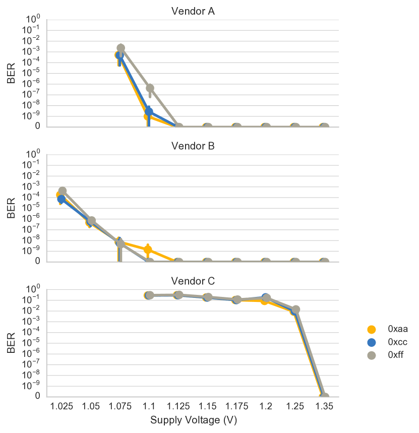
First, the BER increases as we reduce the supply voltage for all three data patterns. We made a similar observation in Section 4.1, which shows that the fraction of errors increases as the supply voltage drops. We explained our hypothesis on the cause of the errors, and used both experiments and simulations to test the hypothesis, in Section 4.2.
Second, we do not observe a significant difference across the BER values from the three different data patterns. We attempt to answer the following question: Do different data patterns induce BER values that are statistically different from each other at each voltage level? To answer this, we conduct a one-way ANOVA (analysis of variance) test across the measured BERs from all three data patterns at each supply voltage level to calculate a p-value. If the p-value is below 0.05, we can claim that these three data patterns induce a statistically-significant difference on the error rate. Table 6 shows the calculated p-value at each supply voltage level. At certain supply voltage levels, we do not have a p-value listed (shown as — or in the table), either because there are no errors (indicated as —) or we cannot reliably access data from the DIMMs even if the access latency is higher than the standard value (indicated as ).
| Supply | Vendor | ||
|---|---|---|---|
| Voltage | A | B | C |
| 1.305 | — | — | — |
| 1.250 | — | — | 0.000000 |
| 1.200 | — | — | 0.029947 |
| 1.175 | — | — | 0.856793 |
| 1.150 | — | — | 0.872205 |
| 1.125 | — | 0.375906 | 0.897489 |
| 1.100 | 0.028592 | 0.375906 | 0.000000 |
| 1.075 | 0.103073 | 0.907960 | |
| 1.050 | 0.651482 | ||
| 1.025 | 0.025167 | ||
Using the one-way ANOVA test, we find that using different data patterns does not have a statistically significant (i.e., p-value 0.05) effect on the error rate at all supply voltage levels. Significant effects (i.e., p-value ¡ 0.05) occur at 1.100V for Vendor A, at 1.025V for Vendor B, and at both 1.250V and 1.100V for Vendor C. As a result, our study does not provide enough evidence to conclude that using any of the three data patterns (0xaa, 0xcc, and 0xff) induces higher or lower error rates than the other two patterns at reduced voltage levels.
Appendix C SPICE Simulation Model
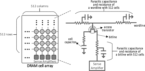
We perform circuit-level SPICE simulations to understand in detail how the DRAM cell arrays operate at low supply voltage. We model a DRAM cell array in SPICE, and simulate its behavior for different supply voltages. We have released our SPICE model online (volt-github, ).
DRAM Cell Array Model. We build a detailed cell array model, as shown in Figure 22. In the cell array, the DRAM cells are organized as array, which is a common organization in modern DRAM chips (vogelsang-micro2010, ). Each column is vertical, and corresponds to 512 cells sharing a bitline that connects to a sense amplifier. Due to the bitline wire and the cells that are connected to the bitline, there is parasitic resistance and capacitance on each bitline. Each row consists of 512 cells sharing the same wordline, which also has parasitic resistance and capacitance. The amount of parasitic resistance and capacitance on the bitlines and wordlines is a major factor that affects the latency of DRAM operations accessing a cell array (lee-hpca2013, ; lee-sigmetrics2017, ).
Simulation Methodology. We use the LTspice (ltspice, ) SPICE simulator to perform our simulations. To find the access latency of the DRAM operations under different supply voltages, we build a DRAM cell array using technology parameters that we derive from a DRAM model (vogelsang-micro2010, ) and from a process technology model (ptm, ; zhao-isqed2006, ). By default, we assume that the cell capacitance is and the bitline capacitance is (vogelsang-micro2010, ). The nominal is 1.35V, and we perform simulations to obtain the latency of DRAM operations at every 25mV step from 1.35V down to 0.9V. The results of our SPICE simulations are discussed in Section 4.1 and 4.2.
Appendix D Spatial Distribution of Errors
In this section, we expand upon the spatial locality data presented in Section 4.3. Figures 23, 24, and 25 show the physical locations of errors that occur when the supply voltage is reduced for a representative DIMM from Vendors A, B, and C, respectively. At higher voltage levels, even if errors occur, they tend to cluster in certain regions of a DIMM. However, as we reduce the supply voltage further, the number of errors increases, and the errors start to spread across the entire DIMM.
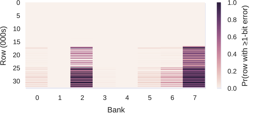
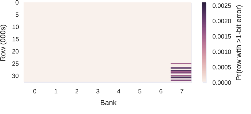
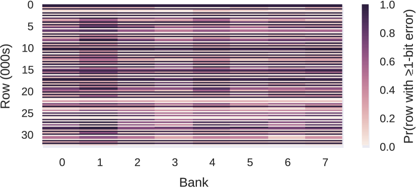
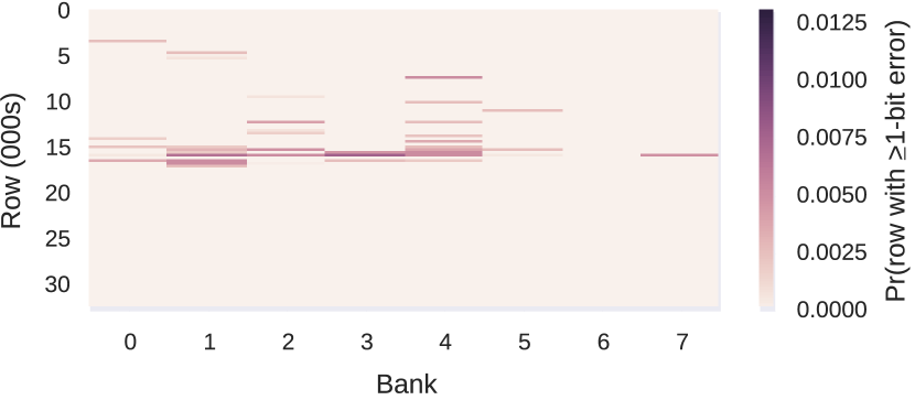
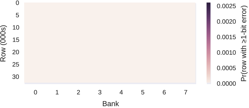
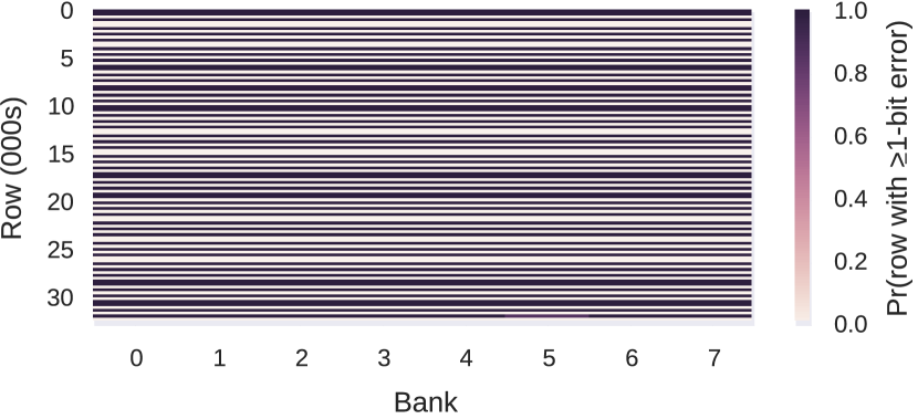
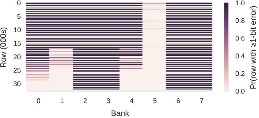
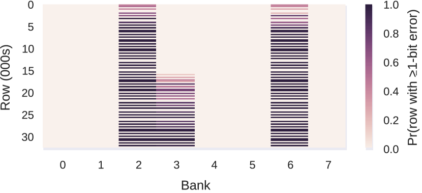
Appendix E Full Information of Every Tested DIMM
Table E lists the parameters of every DRAM module that we evaluate, along with the we discovered for each module based on our experimental characterization (Section 4.1). We provide all results for all DIMMs in our GitHub repository (volt-github, ).
| Vendor | Module | Date∗ | Timing† | Organization | Chip | |||||||
| (yy-ww) | Freq (MT/s) | tRCD (ns) | tRP (ns) | tRAS (ns) | Size (GB)‡ | Chips⋆ | Size (Gb) | Pins | Die Version§ | Vmin (V)∘ | ||
| A | 15-46 | 1600 | 13.75 | 13.75 | 35 | 2 | 4 | 4 | 16 | 1.100 | ||
| A | 15-47 | 1600 | 13.75 | 13.75 | 35 | 2 | 4 | 4 | 16 | 1.125 | ||
| A | 15-44 | 1600 | 13.75 | 13.75 | 35 | 2 | 4 | 4 | 16 | 1.125 | ||
| A | 16-01 | 1600 | 13.75 | 13.75 | 35 | 2 | 4 | 4 | 16 | 1.125 | ||
| A | 16-01 | 1600 | 13.75 | 13.75 | 35 | 2 | 4 | 4 | 16 | 1.125 | ||
| A | 16-10 | 1600 | 13.75 | 13.75 | 35 | 2 | 4 | 4 | 16 | 1.125 | ||
| A | 16-12 | 1600 | 13.75 | 13.75 | 35 | 2 | 4 | 4 | 16 | 1.125 | ||
| A | 16-09 | 1600 | 13.75 | 13.75 | 35 | 2 | 4 | 4 | 16 | 1.125 | ||
| A | 16-11 | 1600 | 13.75 | 13.75 | 35 | 2 | 4 | 4 | 16 | 1.100 | ||
| A Total of 10 DIMMs | A | 16-10 | 1600 | 13.75 | 13.75 | 35 | 2 | 4 | 4 | 16 | 1.125 | |
| B | 14-34 | 1600 | 13.75 | 13.75 | 35 | 2 | 4 | 4 | 16 | 1.100 | ||
| B | 14-34 | 1600 | 13.75 | 13.75 | 35 | 2 | 4 | 4 | 16 | 1.150 | ||
| B | 14-26 | 1600 | 13.75 | 13.75 | 35 | 2 | 4 | 4 | 16 | 1.100 | ||
| B | 14-30 | 1600 | 13.75 | 13.75 | 35 | 2 | 4 | 4 | 16 | 1.100 | ||
| B | 14-34 | 1600 | 13.75 | 13.75 | 35 | 2 | 4 | 4 | 16 | 1.125 | ||
| B | 14-32 | 1600 | 13.75 | 13.75 | 35 | 2 | 4 | 4 | 16 | 1.125 | ||
| B | 14-34 | 1600 | 13.75 | 13.75 | 35 | 2 | 4 | 4 | 16 | 1.100 | ||
| B | 14-30 | 1600 | 13.75 | 13.75 | 35 | 2 | 4 | 4 | 16 | 1.125 | ||
| B | 14-23 | 1600 | 13.75 | 13.75 | 35 | 2 | 4 | 4 | 16 | 1.125 | ||
| B | 14-21 | 1600 | 13.75 | 13.75 | 35 | 2 | 4 | 4 | 16 | 1.125 | ||
| B | 14-31 | 1600 | 13.75 | 13.75 | 35 | 2 | 4 | 4 | 16 | 1.100 | ||
| B Total of 12 DIMMs | B | 15-08 | 1600 | 13.75 | 13.75 | 35 | 2 | 4 | 4 | 16 | 1.100 | |
| C | 15-33 | 1600 | 13.75 | 13.75 | 35 | 2 | 4 | 4 | 16 | 1.300 | ||
| C | 15-33 | 1600 | 13.75 | 13.75 | 35 | 2 | 4 | 4 | 16 | 1.250 | ||
| C | 15-33 | 1600 | 13.75 | 13.75 | 35 | 2 | 4 | 4 | 16 | 1.150 | ||
| C | 15-33 | 1600 | 13.75 | 13.75 | 35 | 2 | 4 | 4 | 16 | 1.150 | ||
| C | 15-33 | 1600 | 13.75 | 13.75 | 35 | 2 | 4 | 4 | 16 | 1.300 | ||
| C | 15-33 | 1600 | 13.75 | 13.75 | 35 | 2 | 4 | 4 | 16 | 1.300 | ||
| C | 15-33 | 1600 | 13.75 | 13.75 | 35 | 2 | 4 | 4 | 16 | 1.300 | ||
| C | 15-33 | 1600 | 13.75 | 13.75 | 35 | 2 | 4 | 4 | 16 | 1.250 | ||
| C Total of 9 DIMMs | C | 15-33 | 1600 | 13.75 | 13.75 | 35 | 2 | 4 | 4 | 16 | 1.300 | |
| The manufacturing date in the format of year-week (yy-ww). For example, 15-01 indicates that the DIMM was manufactured during |
| the first week of 2015. |
| The timing factors associated with each DIMM: |
| : the channel frequency |
| : the minimum required latency for an ACTIVATE to complete |
| : the minimum required latency for a PRECHARGE to complete |
| : the minimum required latency for to restore the charge in an activated row of cells |
| The maximum DRAM module size supported by our testing platform is 2GB. |
| The number of DRAM chips mounted on each DRAM module. |
| The DRAM die versions that are marked on the chip package. |
| The minimum voltage level that allows error-free operation, as described in Section 4.1. |