A review of advances in pixel detectors for experiments
with high rate and radiation
Abstract
The Large Hadron Collider (LHC) experiments ATLAS and CMS have established hybrid pixel detectors as the instrument of choice for particle tracking and vertexing in high rate and radiation environments, as they operate close to the LHC interaction points. With the High Luminosity-LHC upgrade now in sight, for which the tracking detectors will be completely replaced, new generations of pixel detectors are being devised. They have to address enormous challenges in terms of data throughput and radiation levels, ionizing and non-ionizing, that harm the sensing and readout parts of pixel detectors alike. Advances in microelectronics and microprocessing technologies now enable large scale detector designs with unprecedented performance in measurement precision (space and time), radiation hard sensors and readout chips, hybridization techniques, lightweight supports, and fully monolithic approaches to meet these challenges. This paper reviews the world-wide effort on these developments.
keywords:
semiconductor detectors, tracking detectors, pixel detectors, radiation damage, radiation hard CMOS sensors, hybrid pixelsPACS:
29.40.Wk , 29.40.Gx1 Pixel detectors at the heart of particle physics experiments: demands, challenges and concepts
This article reviews recent advances and future directions in pixel detectors to measure high energy charged particle trajectories in high rate and radiation experiments. A general treatment of pixel detectors can be found in [1]. This review focuses on the on-detector elements, and does not include data acquisition or downstream data processing such as track reconstruction. As there are recent reviews on radiation damage of silicon sensors [2] and on mechanics and cooling of such detectors [3] these topics receive an abbreviated treatment here. The current state of the art is represented by the detectors in operation or under construction at the Large Hadron Collider at CERN, in the ATLAS, CMS, LHC-b, and NA62 experiments.
The ATLAS experiment installed a 3-layer hybrid pixel detector in 2007 [4] and an additional layer at lower radius, inserted within the original detector envelope and therefore called Insertable B-Layer (IBL), in 2014 [5]. The IBL pioneered the use of 3D silicon sensors (in a limited acceptance range) and introduced a new readout integrated circuit (ROIC or readout chip) called FE-I4 [6] with several of the features needed for future high rate detectors.
The CMS experiment installed a 3-layer hybrid pixel detector in 2008 [7], and has replaced it with a new, 4-layer detector in 2017 [8]. The new detector has lower inner radius, significantly lower mass which improves precision, and higher data rate capability needed to cope with increased accelerator luminosity. The upgrade baseline ROIC was redesigned for the outer 3 layers, replacing analog signal readout with on-chip ADCs and digital readout at higher rate [9]. A different ROIC has been designed specifically for the inner layer to handle higher rate and radiation, while keeping to the original footprint. To reduce the mass of the services, radiation hard voltage regulators [10] have been introduced just outside the acceptance, but still inside the CMS inner barrel volume.
The LHC-b experiment is replacing their strip vertex detector with a 26 plane pixel detector (fixed target geometry) [11]. The detector will use triggerless readout at the full 40 MHz collision rate of the LHC. The high data volume will be handled by up to four 5 Gbps serial outputs per ROIC [12], transmitted over high bandwidth copper cables outside the physics acceptance.
The NA62 experiment has installed a fixed target geometry hybrid pixel detector called Gigatracker to measure timing with high resolution (200 ps) as well as position in each pixel [13]. This is a small area detector, but is pioneering the use of per-pixel timing in particle tracking.
The challenges that drive ongoing development can be broadly categorized into scale, intensity, and performance. Particle physics programs demand pixel detectors with larger outer radius to cope with higher rates, and greater length along the beam direction to increase acceptance. Significant development is therefore focused on how to produce pixel detectors with less effort and lower cost. The two main directions are lower cost production of hybrid pixels and diode sensors (chapter 3), and development of monolithic technology in CMOS foundries (chapter 6).
Increasing collider intensity places two main demands on pixel detectors: the ability to store and process greater hit rate per unit area (chapter 4), and higher radiation tolerance (chapters 3, 4, 6). All hits “raining” on a pixel detector unit area must be time-stamped and stored for a trigger latency interval. This means more memory per unit area in the ROIC, which directly translates to a need for a technology with higher logic density (i.e. smaller feature size, following Moore’s Law). Note that the need for higher logic density is not a function of pixel size, but of hit rate per unit area. Smaller pixels are needed to maintain efficiency (to avoid pileup of hits in a single pixel), for resolution (chapter 2), and for radiation tolerance (to keep the leakage current per pixel small). Higher intensity also means that collision events all 'look alike', because every event has a large number of superimposed low energy scatters (pileup), and may or may not have a hard scatter of interest as well, typically with less energy than the sum of the underlying pileup. As distinguishing events of interest becomes more difficult, triggers must increase rate (for a given signal acceptance more background will pass the trigger) and/or use more information, including tracking. Pixel detectors must therefore output much more data (section 4.8).
Achieving larger scale and coping with higher intensity are necessary to increase the physics reach of particle physics experiments. The basic performance of a detector can also improve the physics reach, and therefore, the challenges of scaling and intensity are compounded by the desire to increase performance. Given signal size, sensor capacitance, and device specific transconductance in the ROIC, the pixel front end achievable performance is determined, and actual ROIC’s come close to this limit. From a single pixel perspective, the analog performance limit given a power budget and ROIC and sensor technologies is well understood and achieved by the implemented circuits. New developments to increase performance are therefore looking beyond the basic model of a pixel detector as a collection of individual pixels with an output of 3D space points. Correlations between pixels and measurements with internal degrees of freedom (in addition to the usual spatial coordinates) can be used to improve pattern recognition, suppress background, and even provide input to a trigger system. The main degrees of freedom under study are timing, direction, and cluster shape and charge distribution (see chapter 2).
2 Space–time point resolution
2.1 Demands and current directions
The basic detection mechanism of silicon detectors is the generation and drift of mobile charges (e/h) in a depleted silicon junction. This charge cloud has a rich spatial and temporal structure with some dependence on incident particle type and trajectory as well as existing electric and magnetic fields in the silicon. Silicon tracking detectors have typically had granularities in space and time greater than or equal to the charge cloud deposit, resulting in one 3-D space point per particle crossing a sensor with a fairly coarse arrival time stamp, sufficient to associate the point with a given accelerator collision event. Measurement of the magnitude of the collected charge has also been generally available for pixel detectors, and has been used to improve the 3-D space point precision through interpolation as well as for particle identification through specific ionization measurement.
In current detector development we are starting to see increased space and time granularity, in order to measure and make use of the structure of charge deposits. There are many interesting applications of this extra information beyond pure space points. We will give below a few present or anticipated examples: multi-track to cluster association using machine learning, a angular information from cluster length, 3-D cluster shapes using charge arrival time, and disentangling of multiple interactions from sub-nanosecond hit timing.
To be fully exploited, the trend towards fine granularity in space and time, to resolve the charge deposit structure and even the sequence of particle impacts within a detector, must be accompanied by an evolution of the pattern recognition and track fitting algorithms used. Interestingly, algorithm evolution seems to lag detector development. Currently used techniques are still largely based on space points, with extra information added for specific tasks after space point reconstruction. In this chapter we review the basics of space point reconstruction and extend towards new space-time measurement directions as far as they are known and published today. But we expect to soon see modifications of the conventional, well known formulas to include angle, direction, and time measurements.
In general, the tasks of pixel detectors in HEP experiments can be listed as follows:
-
1.
Pattern recognition and identification of particle tracks at large background and pile-up levels
-
2.
Measurement of primary and secondary vertices;
-
3.
Multi-track separation and vertex identification in the core of (boosted) jets;
-
4.
Momentum measurement of particles (together with other detectors, like strip detectors);
-
5.
Measurement of specific ionization.
Small pixel size keeps the pixel occupancy down at high particle rates (important for item 1) and also leads to good hit resolution. Space point resolutions in the order of 10 m or less have been routinely achieved at least in one dimension. Achieving the best possible resolution is of utmost importance to cope with the above challenges.
Recent developments (e.g. [14]) also address processing of multi-hit pixel clusters as complex objects to exploit directional information and improve the two track resolution, in particular inside the core of jets.
Time resolutions at the 10–100 ps level have not been realized so far with semiconductor tracking detectors. If achieved this will add another measurement dimension which can be exploited for example to distinguish calorimeter jets coming from a hard interaction from those with large pile-up contributions by using the arrival time distribution (being broad for pile-up jets). Precise timing might also allow coincidence measurements e.g. between tracks in the forward and backward regions of a detector.
2.2 Space point and direction measurements
Figure 1 sketches two typical situations for pixel hit clusters. Case (1) represents the case of a particle impinging close to perpendicularly to the pixel module leading to hit clusters of typically one or two pixels. Case (2) represents tracks impinging at steep angles, thus producing larger hit clusters with some directional information when properly treated by reconstruction algorithms, in particular when such clusters appear in several detector layers along a track. Exploiting the hit information this way could become important for hit assignment and track recognition in high track density at the LHC (see for example [14]).
Point measurements
The precision of a space-point measurement enters the momentum resolution in a track measurement with detector layers as given by the Gluckstern formula [15]:
| (1) |
where is transverse momentum in GeV/c, is the radial length in m, magnetic field in T, is the particle electric charge in elementary units, is the point resolution of the detectors in m, and is assumed to be large in this approximation. Important for a precise momentum measurement is the point resolution, but also (quadratically) the total length of the tracker and the bending field . The multiple scattering (MS) contribution for a number of detector layers can be written as
| (2) |
where is the tracker length projected onto the plane perpendicular to the magnetic field, and is the total material thickness traversed by a particle incident with polar angle with respect to the beam, in units of the radiation length. is a factor depending on the number of layers: for the minimum of three layers to measure a circle; it approaches for (continuous scattering).
Even though the hard collisions at the LHC produce high energy jets, low momentum tracks around and below 1 GeV/c transverse momentum play an important role, especially in the forward direction. For example, efficient jet tagging - jets in general and b-jets in particular - and suppression of pile-up contributions by primary vertex identification suffer from imprecise detection of low momentum particles. For the HL-LHC, low tracks will become even more important as pile-up increases. This renders low mass (low ) extremely important.
Similarly, the precision of secondary vertex measurement with an layer tracker can be expressed by the impact parameter resolution (here in linear extrapolation):
| (3) |
where the first term results from the extrapolation from the tracker to the primary vertex with being the ratio of the extrapolation distance to the tracker length. The point resolution enters linearly. For a pixel detector with four layers as in ATLAS, at radii between 3.3 cm and 12.3 cm and with a point resolution of about 10 m, this yields m without multiple scattering.
The second term is due to multiple scattering approximated by assuming extrapolation from the first layer to the primary vertex, the slope of which is smeared by multiple scattering, with being the multiple scattering angle [16]:
| (4) |
and the distance of the first pixel layer to the primary interaction vertex. For a 4-layer geometry like in ATLAS and a material thickness of typically around 3% the multiple scattering contribution to the resolution yields
| (5) |
Spatial resolution also impacts pattern recognition performance in complex interplay with pixel occupancy, material thickness, and layout. However, pattern recognition algorithms are outside the scope of this review.
Space-point reconstruction methods
In designing a pixel detector one selects the (initial) amount of charge sharing. The tuning parameter for a given planar sensor thickness is the ratio of the Lorentz angle (the deviation from perpendicular to the sensor surface of the drift path of charges in a magnetic field [17]), to the tilt angle of the module with respect to perpendicular particle passage. While charge sharing between pixels allows for better spatial resolution by charge interpolation, a signal decrease caused by irradiation during the detector’s lifetime demands minimal charge sharing. Whether collected charge causes a hit also depends on the pixel threshold. Noise deteriorates the precision of reconstruction and causes spurious hits.
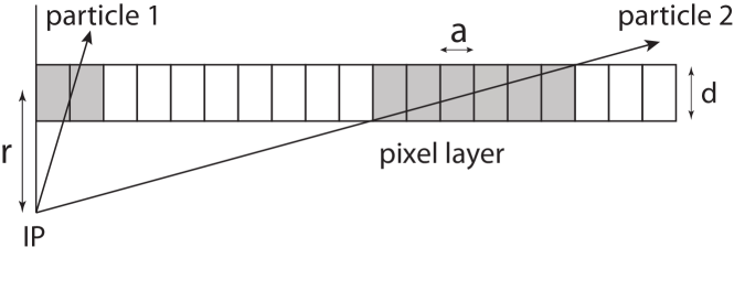
For the present LHC pixel detectors with relatively large pixels, covering mainly central rapidity and not having too steep incidence angles, the number of hits in a cluster from a single track is rarely greater than 2. At large incidence angles in the forward regions of a barrel pixel detector or in the future with smaller pixel sizes, the cluster distribution can become much larger and this information can also be exploited (see below).
Resolutions achievable with classical space point reconstruction methods can be classified as follows:
-
1.
For single hit clusters - independent of having binary (yes/no) or analog origin - resolution is given by the well-known pitch/ RMS resolution assuming a flat prior distribution of track position within the pixel (most conservative assumption). For an arbitrary given cluster size and track direction the resolution still is constant and is determined by the RMS of the prior track distribution that can produce a cluster of this size. For large clusters, high spatial resolution is possible even with binary readout, due to the averaging of many pixels.
-
2.
Analog hit information can be obtained at the expense of a larger total data volume (see e.g. [4][18] for ATLAS) or by processing the analog pulse off the module as is done in CMS [7]. In this case the reconstructed hit position can be obtained e.g. by the centre of gravity method
(6) where the and are the signal and noise fractional weights, respectively, and is the center of each individual pixel in the cluster. The achievable resolution is:
(7) where denotes uncorrelated noise and is the number of hit pixels [19, 20].
-
3.
If two hit clusters is the most common case for pixel detectors the -reconstruction method [21, 22] is optimal for space reconstruction of Gaussian charge clouds, since detector effects are automatically included. For two adjacent left and right electrodes the function
(8) constructed from measured signals is position dependent, , and the hit position is obtained from the inverse :
(9) where is the probability distribution (with normalization ) of hits vs resulting from uniform illumination (random distribution), and is the channel pitch. Including noise (fractional, i.e. in units of the signal) (9) becomes [19][20]:
(10) with . Obviously, a steep response function yields the best resolution, given by:
(11) where the second term vanishes for uncorrelated noise, .
By using analog information either directly (CMS) or via a Time over Threshold (ToT) digitization (ATLAS), resolutions as shown in table 1 have been obtained (references in table). The ToT method is explained in section 4.6.
| Experiment | R/O method | pitch [m] | inc. angle | [m] |
|---|---|---|---|---|
| ATLAS [23] | binary/ToT | 250 | 0∘ | 66.5 |
| ATLAS [23] | ToT | 50 | 0∘ | 10 |
| ATLAS [4] | ToT | 50 | 10∘ | 7 |
| CMS [24] | analog | 150 | 0∘ | 44 |
| CMS [24] | analog | 150 | 30∘ | 21 |
| CMS [24] | analog | 100 | 0∘ | 9.4 |
Limitations to the space point resolution of a pixel detector
When aiming for ultimate spatial resolutions with hybrid pixel detectors the following limitations are encountered:
-
1.
Since for hybrid pixels the chip’s pixel area must match the sensor’s pixel area the smallest pixel size is determined by the amount of CMOS electronics needed to amplify, discriminate, and process the hit information in the area occupied by the pixel cell. Third generation chips for high hit rate achieve about m2 or m2, limited by logic density as explained in section 4.
-
2.
The signal of a traversing MIP (Minimum Ionizing Particle) spreads due to diffusion according to , where is the diffusion constant, the drift distance to the electrode and the drift velocity. For a typical detector thickness of 150–200m, becomes 4–8 m. Hence pixel pitches well below this (at the same sensor thickness) would lead to excessive charge sharing.
- 3.
In-pixel decoding
It has been proposed [26] to effectively achieve smaller pixel size by encoding and decoding the pixel sensor cell by means of 'smart sensors' when using depletable substrates with a CMOS electronics layer (see also section 6).
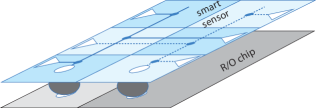
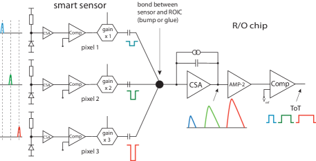
Figure 2 shows the principle. Two pixels of the readout chip (e.g. FE-I4 with 50 m 250 m each) match six (sub-)pixels of the smart sensor with sizes 33 m 125m. Three sub-pixels at a time are connected to one of the two FE-I4 inputs via AC coupling, either by a capacitor included in the sensor pixel plus DC connection (bump bonding) to the corresponding FE-I4 chip pixel, or by gluing the sensor chip/wafer to the FE-I4 wafer, in which case the coupling is also capacitive. The digital (voltage) output pulse of the smart sensor is capacitively coupled into the CSA input of the readout chip. The three digital output stages of the sensor pixels can be programmed with three different gains (high, medium, low) such that digital pulses of different height are capacitively coupled to the input of FE-I4 depending on which of the sub-pixels has been hit. Further processing of the pulse by the FE-I4 amplification and discrimination stages turns different pulse heights at its input into different ToT values at the output. Hence the sub-pixel hit by the MIP is finally decoded from its ToT value. Test beam measurements demonstrated the functionality of the method [27, 28].
Directional information from hit clusters
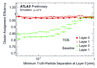
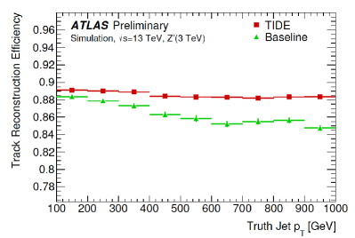
Multivariate algorithms like artificial neural nets (ANN) have now also entered the area of hit/cluster to track association for improved track reconstruction in high multiplicity environments. The single hit precision is not the only figure of merit to tune. One must also optimize the capability of cluster shape analysis (especially for inclined tracks) and the analysis of pattern information of clusters from dense tracks over several layers. For example in [14] it is shown how successive employment of ANNs can improve (a) the association of merged clusters to tracks, (b) track reconstruction inside the core of (boosted) jets, and (c) heavy flavour and -jet identification. The amount of charge per pixel, for instance provided by the ToT technique [4], and a precise knowledge of the pixel coordinates is already sufficient as input for the ANN to identify merged clusters efficiently. The emission of -rays and secondary interactions of tracks prevent a perfect ANN performance. The approach benefits from knowing the incident angle of tracks, estimated from the coordinates of modules with respect to the beam spot, and from correlating information from consecutive layers of the pixel detector [14]. Figure 3(a) demonstrates using simulation the gain in cluster assignment efficiency using this technique on a sample of simulated decays. Figure 3(b) shows the improvement in tracking efficiency inside dense jet-cores obtained using the ANN-based improved merger identification. Improvement in high- heavy flavour identification of 7–13% (b-tagging and b-jet identification) and of 5% in 3-prong -jets above GeV is the result [14].
2.3 Time measurement
The charge collection time, i.e. the time until the arrival of the last electron at the pixel electrode, typically is in the order of 3–10 ns, depending on sensor thickness and E-field. The induced current pulse at the electrode instantly starts with the particle passage and consists of the incoherent sum of induced pulses from each carrier’s path towards (e-) and away (h+) from the pixel electrodes. The individual contributions are weighted by the pixel weighting field (see e.g. [29, 1, 19]) leading to the fact that the carriers’ paths close to the pixel implant have the strongest contributions to the signal. In a typical pixel detector the current pulses are integrated by the input stage of the subsequent readout chip, a charge sensitive amplifier (CSA). While such a readout method has low noise performance111Typical noise values are on the order of 150 e- for the present LHC detectors [4, 7] and will be around 80 e- for future detectors with smaller pixels [30]. it does not allow timing measurements at or below 100 ps, values at which timing becomes interesting for high energy particle detection.
For a time coordinate measurement to reach equivalent spatial resolutions in the cm to mm regime, time resolutions of the order of a few tens of picoseconds are needed. To achieve this with pixel detectors, where charge collection times are in the ns range, is a real challenge. Recently, amplification structures in silicon have been brought forward to cope with these demands [31, 32, 33]. Potential benefits are the suppression of pile-up jets by recognizing the time-wise association of tracks to a primary vertex.
LGAD structures
In order to reach into the picosecond timing regime with silicon detectors, in-silicon amplification can be employed. Avalanche generating silicon based devices have been developed in the context of photodetectors (see for example [34],[35],[36]). They can be distinguished by their operation mode, either as linear avalanche photodiodes (APD) operating in a linear amplification mode or as so-called Geiger APDs operating near the breakdown point thus sensing a light pulse by a large breakdown pulse with follow-up recovery time. Timing in Geiger-mode operation will be governed by the time jitter introduced by the breakdown process (multiplication jitter), similar to the case for gaseous detectors where fast timing is addressed for example with RPCs (resistive plate chambers) [37]. Another approach has been chosen by [31], namely by operating avalanche silicon diodes at a low gain operation point, so-called Low Gain Avalanche Diodes, LGADs.

In order to create precise time stamps, fast and large signals and low noise are needed. The slew rate can serve as a figure of merit, defined as
| (12) |
Figure 4 shows a principal cross section of an LGAD structure [38]. In a bulk, faced on both surfaces by the usual very highly doped222We here adopt the notation p++ for cm3, likewise for . and electrodes rendering the structure of the detector, an additional, highly doped layer (cm3)) is implanted immediately underneath the electrode, thus creating a very local high electric field of up to 300 kV/cm. This is the multiplication layer amplifying all arriving electrons by a factor of the order of 10-20, thereby creating secondary e/h-pairs.

The signal induced on the electrodes therefore has several components (see fig. 5):
-
1.
Electrons and holes drifting from the point of creation along the track towards their respective collection electrodes. The individual e/h parts of this contribution are small before amplification takes place and end when the last carriers have arrived at their respective electrodes.
-
2.
Amplification electrons created in the multiplication layer reach the top electrode (fig. 4) almost instantaneously and their contribution to the induced signal current is close to negligible, because - according to the Shockley-Ramo theorem [40, 41] -
with = weighting field and = drift velocity, there is almost no current contribution since the drift duration for electrons is quasi non-existent and ending before the next primary electrons reach the amplification layer.
-
3.
By contrast, the multiplied holes drifting from the amplification layer towards the backside contribute to as long as they are drifting. Their contribution adds up, provided that the weighting field is formed such that it does not suppress contributions from distant holes too much. This implies that the pixel/pad implant widths must be large compared to the implant distances and should be in the same order of magnitude as the detector thickness.
As can be seen from fig. 5, a large slew rate and hence fast timing requires fast (primary) electron arrival at the amplification zone together with fast (amplified) hole movement away. Short bunching and fast movement in high fields ( 20 kV/cm) benefit from thin sensors.
The time resolution has several contributions [42]:
The first term represents time walk introduced by different signal pulse heights due to different energy deposits coming from Landau fluctuations in the energy loss process and its resulting pulse height fluctuations at the discriminator input. Minimization of this term is possible e.g. by employing a constant fraction discrimination or a ToT correction architecture in the readout. The second term is noise jitter, i.e. time fluctuations due to noisy signals. Both contributions are made small when large slew rates are achieved. An irreducible contribution comes from fluctuations resulting from non-uniform depositions of charge along the particle track moving towards the amplification junction, hence causing an intrinsic jitter in the arrival time (third term). Fluctuations from secondary ionizations and from the amplification process enter here as well. The thinner the detector the less disturbing is this effect. An additional 4th contribution is signal distortion due to non-uniform weighting field regions and variations in (non-saturated) drift velocities. The final term is time fluctuations due to uncertainties in the time digitization. It is assumed that the latter can be made negligible (below 10 ps) with GHz TDCs.
The key ingredients for fast timing and small time jitter are thin detector substrates ((50 m)) providing three essential benefits:
-
1.
larger slew rate (1.6 slew rate increase going from d = 100 m to 50 m at a gain of 20),
-
2.
better bulk radiation hardness,
-
3.
smaller arrival time fluctuations due to a shorter charge deposition path.
In fig. 6(a) the slew rate is plotted against the diode thickness for different gains assuming an input capacitance of 2 pF [38].
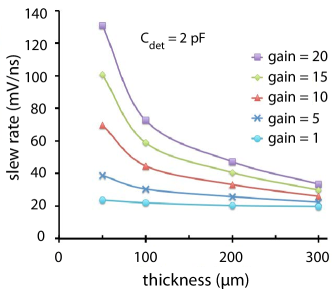
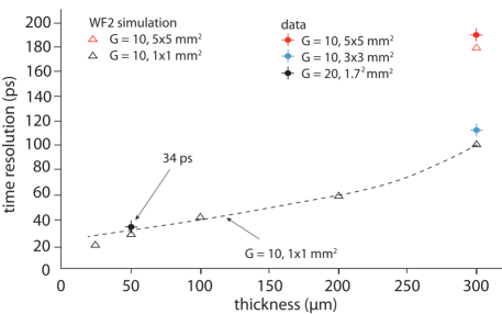
It is evident that large slew rates can be obtained with thin detectors and sufficient gain ( 10). Much higher gains compromise the S/N ratio, because bulk shot noise is also amplified by the amplification structure (called excess noise) such that there is an optimal gain for maximum signal-to-noise (see for instance [36] or [42]).
Prototype LGAD structures have been fabricated [38, 43] with relatively large pads (from 88 mm2 to 11 mm2), rather than pixels, mainly to validate the underlying models and simulations of the achievable time resolution. Figure 6(b) shows the predicted time resolution by simulations [39] as a function of the detector thickness. At the right hand side measured data from 300 m thick LGAD pad detectors are compared with simulations. Extrapolation to thin detectors yields time resolutions in the order of 30 ps. Very thin detectors have only recently become available. In a test beam measurement with 180 GeV pions, a 50m LGAD sensor with 1.21.2 mm2 pads has been characterized, achieving 34 ps time resolution at a bias voltage of 200 V [44], in excellent agreement with predictions from weighting field simulations (fig. 6(b)).
A major concern for the use of LGADs at the HL-LHC is their performance in high radiation areas. Apart from the usual effects caused by radiation in silicon detectors like leakage current increase and deteriorated charge collection efficiency, effective doping changes play a sensitive role. Since the metallurgical junction providing the amplification gain requires p-doping concentrations of order of 1016cm-3, radiation induced acceptor removal will have detrimental effects upon the gain. Detailed radiation studies are currently ongoing [42], including very thin sensors ( 50 m) and devices with gallium substituted as p-dopant in the amplification implant instead of boron, to reduce interstitial capture that scales with atomic mass [45]. Another proposed method is to use carbon-enriched wafers with (abundant) carbon being trapped by silicon interstitials rather than boron.
3 Pixel sensors and hybridization
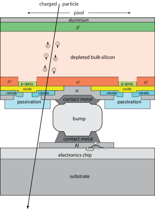
'Hybrid pixels' including a sensor (electronically passive) and a readout chip as separate entities (fig. 7) currently are the state-of-the-art technology for large scale pixel detectors in most particle physics experiments [1]. For both parts, the radiation requirements at LHC-type experiments constitute a challenge which is addressed by dedicated R&D and process engineering techniques.
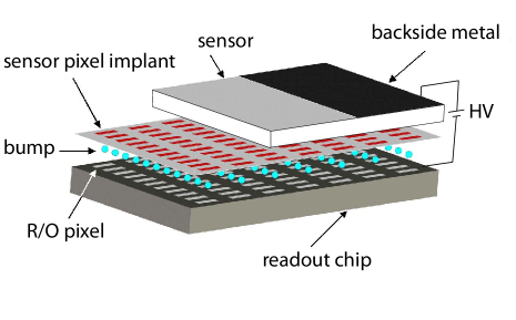
In this chapter we describe passive sensor types used in hybrid pixel assemblies, to be contrasted to CMOS active monolithic sensors that integrate electronics circuitry and sensor, described in chapter 6. The mechanical and electrical mating of sensor and readout chip, called hybridization, requires state-of-the-art processing technologies, also described in this chapter (section 3.3). The hybridization mating partner, the readout chip is described in detail in chapter 4.
After the success of planar sensors (section 3.1) in LHC run-1, having planar pixel implants at one side of the sensor and being fabricated using 4′′ sensor wafer technologies, the desire for large detector modules at affordable cost has fueled the move to 6′′ and possibly even 8′′ wafer sensor technologies. In line with this a better understanding of radiation damage effects and radiation hard sensor device engineering became a research branch on its own, coordinated within the CERN RD50 collaboration [45].
Radiation hard device engineering includes using silicon with increased oxygen content supplied in the growth process [48, 49, 50] and operation at low-temperature, both employed to reduce the damage’s impact on the detector performance. Furthermore, so-called 3D-silicon sensors [51] (see section 3.2) have been developed having vertically structured electrodes fabricated within the volume of the silicon substrate (fig. 11). Their main feature is a better ratio of ionization thickness to charge collection distance than for planar sensors. After an operation performance demonstration in the first pixel upgrade of ATLAS (Insertable B-Layer, IBL [5]), an innermost pixel barrel layer at a distance of 3.5 cm from the interaction point, equipped with 25% 3D-Si sensors (at high ) and 75% planar pixel sensors, both sensor types now compete for the HL-LHC upgrade as pixel sensors for the radiation hot areas near the interaction point.
A challenge for both sensor types imposed by the radiation fluences of 1016 neq/cm2 is the small foreseen sensor thickness (100–150 m) and the correspondingly increased handling and hybridization difficulty.
Another advance in cost reduction of sensor wafers has been made possible by the availability high quality p-substrate material (2 kcm). With n-in-p type sensors cost-efficient single sided processing suffices for fabrication while maintaining electron collection (n-type pixels). During the initial LHC pixel development period (late 1990s) high ohmic p-type sensor wafers were not favoured, largely for reasons of historical development333Single sided Si sensor development had begun using n-substrate material with hole collection on p-electrodes. For radiation tolerance reasons electron collection became favored leading to -in- structures with double sided processing. For n-in-p sensors it then has taken time to develop n-side multi-guard-ring structures and reliable HV bias isolation from the electronics before high quality p-type sensors were fabricated., and -in- planar pixel sensors have been used instead, requiring processing steps on both sides of the wafer.
With CMOS technology vendors becoming more open to smaller market customers, the use of high ohmic 8′′ wafers fabricated in (much lower cost) CMOS processing lines become options for (planar) sensor options (see section 3.1).
Currently, therefore, the trend in hybrid pixel module development goes to large readout chips and thin sensors, preferentially using p-type bulk material, all being beneficial for cost, radiation tolerance, and detector mass, while the handling and hybridization demands increase. The latter together with the increased interest for large area coverage using pixel detectors also revived collaboration with industry to develop lower cost hybridization techniques with thinner wafers/chips.
3.1 Planar pixel sensors
The proven standard of planar pixel sensors at the LHC experiments has pixel implants on -type substrate material as shown in fig. 8(a). The fabrication demands double-sided processing. The negative bias potential on the backside is brought down to zero potential at the sensor edge by a many guard ring structure implanted on the backside. The pn-diode is initially on the unstructured backside of the sensor, changing to the electrode side after radiation has turned the bulk’s doping into effectively p-type (type inversion). For typical substrate resistivities of 2–5 kcm, this happens after fluences of some neq/cm2. After type inversion the depletion zone grows from the electrode side into the bulk guaranteeing that signals induced by moving charges can be sensed on the pixels even if the substrate is no longer fully depleted, i.e. not depleted at the side opposite to the pixels. To prevent an electron accumulation layer from short circuiting the -in- pixels before type inversion, shallow -doping is used in between the pixel electrodes, with a smoothly changing doping profile preventing high field corners. Details are given in [1].
With increasing radiation fluence the bias voltage needed for sufficient depletion must be increased, eventually reaching values of more than 500 V at fluences around and beyond neq/cm2. For the innermost layers close to the interaction point this corresponds to detector lifetimes of only a few years at current LHC luminosity.
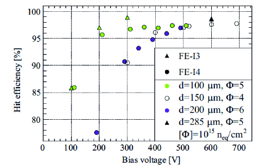
The development of planar sensors for the LHC high luminosity upgrade has therefore concentrated on tailored designs guaranteeing high fields and sufficiently large depletion depths after fluences of up to and above neq/cm2. This has been achieved using n+ pixel implants in p-substrate material and thin (100-150m) sensors operated at bias voltages of 500-700 V [52]. While providing smaller signals per MIP, the benefits of thin sensors are higher electric fields as well as shorter and faster electron collection for a given bias voltage and hence better radiation tolerance. Thin 6′′ or even 8′′ sensor wafer production is enabled by techniques employing SOI or Si-Si handling wafers, or by thinning (e.g. by cavity etching) and forming a back side ohmic contact at low temperature after the front side processing is complete. Currently the limit in thickness is considered to be around 50 m [53].
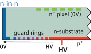
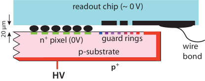
The guard ring designs, bringing down the potential from the bias implants (HV) to the pixel implants (0 V), play an important role in optimizing the breakdown behaviour of sensors after irradiation. The number of rings, implant distance and size, as well as metal overhangs for vertical field suppression are the parameters to optimize. Optimal performance regarding radiation tolerance has been obtained [53] with 10–11 rings with metal overhangs on both sides of the implant over a total length of 350 m. The distance from the edge to the active part of the sensor is 400 m. Other designs trying to minimize this distance make use of etched and doped edges, called active edges, reaching values down to about 50m [54].
Figure 8(a) shows a planar pixel design as used in present LHC hybrid pixel detectors (200 m thick, -in- design) compared to a thin -in- design (fig. 8(b)). Note that, if cost saving single sided processing is to be used, the guard ring structure needs to be placed on the electrode side and is thus in very close proximity (m) to the readout chip, a challenge for the design. Dedicated passivation with BCB (benzocyclobuthene) or parylene, however, appears to be able to solve this issue [55]. Figure 8(c) shows that high hit efficiencies can be achieved after irradiation with thin sensors for bias voltages in excess of 500 V.
Use of 8 wafers and CMOS foundries
It is also possible to fabricate planar sensors on 8′′ wafers using high ohmic substrates either in dedicated sensor fabrication facilities or by employing CMOS foundries, as has been successfully demonstrated for strip and pixel sensors [56, 57]. This has the following advantages compared to the standard small volume sensor fabrication:
-
1.
Large volume production lines can be used with price advantages, suited in particular for large area detectors, e.g. in outer tracking layers at collider experiments.
-
2.
Wafer sizes of 8′′ or 12′′ are a commercial standard allowing large sensors when stitching over reticle boundaries is applied. Stitching is a method to cross the boundaries between reticles of a wafer with metal lines and implant areas, widely applied in the digital imaging industry [58]. Current reticle sizes are about 2525 mm2. By putting individual building blocks of a design separately (rather than together) on the reticle/mask one can join them together over the reticle’s boundary by special lithographic programming, thus allowing IC fabrication of sensor sizes much larger than the reticle area of the CMOS process.
-
3.
The wafers can be purchased with solder bumps already provided by the CMOS vendor (e.g. so-called C4 bumps [59], pitch m).
-
4.
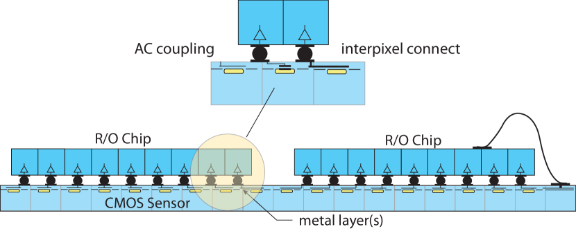
One or two metal layers can be exploited for AC coupling of the sensor cell to the amplifier and for connection redistribution, e.g. to connect amplifier inputs to pixels in areas not covered 1:1 by readout chip cells (regions in between readout chips).
A sketch illustrating some features employing passive CMOS sensors is shown in fig. 9.
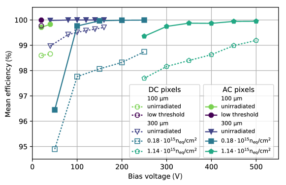
Measurements on passive CMOS pixel sensors, 100 m and 300 m thick, irradiated to fluences of 1.1 neq/cm2 have shown lab and test beam performance equal to those of planar sensors fabricated in dedicated sensor production lines [60]. Figure 10 shows the mean hit efficiency as a function of bias voltage measured with 3.2 GeV electrons for DC and AC coupled passive CMOS sensors bonded to the ATLAS readout chip FE-I4. In particular the AC-coupled devices show excellent performance without any efficiency losses. The DC devices are a bit less efficient due to the area taken by the punch-through dot for biasing of the pixel implants.
3.2 3D-Si sensors
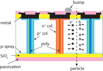
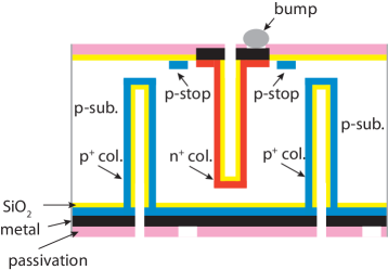
So-called 3D-silicon sensors have been developed since the late 1990s [51, 61] featuring columnar electrode implants driven into the Si substrate perpendicular to the sensor surface (fig. 11). The electrode distance is made smaller (50m) than the typical sensor thickness (200-250m), thus rendering a shorter average drift distance for particles impinging on the sensor face than in the case of planar sensors (compare fig. 7(a) to fig. 11(a)). In addition, high drift fields are obtained with still moderate bias voltages. Both these facts result in an increased radiation tolerance due to a reduced trapping probability.
The 3D-Si technique has been developed over many years. The first structures were fabricated at Stanford (later also at Oslo) [62] using single sided processing with columns reaching completely through the bulk (called 'full-3D'and shown in fig. 11(a)). Further development by CNM [63] and FBK [64] of sensors used in the ATLAS IBL detector, resulted in double-sided 3D designs with columns entering the bulk from both sides, either in full-3D or in partial-3D (shown in fig. 11(b)). The process fabricates about 10 m diameter columns by etching, followed by a 1 m polysilicon layer covering the inside of the etched holes, then passivated by a wet oxide [63]. In addition the sensor edges can be fabricated with active edge implants thus rendering sensors with an unrivaled active area fraction [65].
More details on etching holes into silicon can be found in section 3.5.
Within the ATLAS IBL detector 3D-Si pixel sensors have been proven to operate well in a running experiment [5]. After two years of operation the performance of 3D-Si pixel modules in terms of operation characteristics (signal, noise, threshold settings, in-time efficiency) are on par with planar pixel modules operated with significantly higher voltages [68].
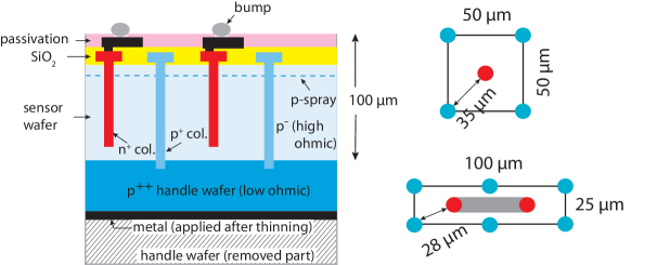
Current developments motivated by HL-LHC demands [69, 63, 70, 71] target the following goals to optimize radiation hardness, granularity, material budget, and processing costs [71]: (a) thin sensors (100 m) on 6′′ wafers, (b) narrower electrodes (5 m), (c) shorter electrode spacing (30 m), and (d) very slim (50 m) or active edges. Single sided processing is preferred providing cost benefits. An advanced design [71] is shown in fig. 11(c). A thin, highly resistive (p-type) sensor wafer is supported by a low ohmic (p++) handle wafer that can be backside thinned after processing. While the p+ columns are deep etched through to the handle wafer where they receive their electric potential, the n+ columns stop about 15 m short from the handle wafer. In addition to cost and yield advantaged of single-sided processing, studies have shown that the trade-off between signal efficiency and breakdown performance favors partial depth n-columns (not extending all the way through the thickness) [72]. At the top surface isolation of the n-columns is achieved by a p-spray layer preventing the electron accumulation layer underneath the oxide from creating shorts. Sensors are designed to meet the currently planned pixel area sizes of m2 or m2, as shown on the right of fig. 11(c). The performance of such designs has been shown to yield high breakdown voltages before and after irradiation [73].
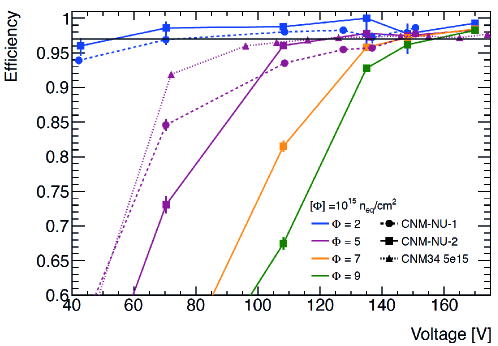
The hit efficiency obtained with 3D-Si structures designed by CNM [69] is demonstrated in fig. 12 for fluences of up to 0.9neq/cm2 [69]. A 97% efficiency plateau is reached with comparatively low bias voltages of 150 V even at the highest fluences, with the missing 3% being largely due to tracks with straight incidence into the column structures, a case not possible for tracks from actual LHC collisions. Smaller implant pitches with lower voltages for the same field strength also reduce power dissipation due to leakage currents after irradiation. This creates some safety margin against thermal runaway, not completely negligible even at the moderate bias voltages of 3D-Si sensors [74].
3D-Si sensors therefore are a strong contender for hybrid pixel modules for the innermost pixel detector layers at the HL-LHC. It should be noted, however, that the fabrication process does is currently low volume. making it unlikely to cover large areas ( m2) with this technology choice.
3.3 Bonding techniques
Wafer- and chip-bonding as well as 3D-integration technologies are in widespread demand in the semiconductor industry sector of IC module assembly and stacking. Many techniques exist that are suitable for a large variety of applications and given fabrication constraints. A large amount of literature is available, reviewed and summarized for example in [75, 76, 77].
For hybrid pixel detectors, the mating of readout chips to substrate (sensor) plates or substrate wafers is the main application of bumping/flip-chipping and 3D-integration techniques. The overriding demands in these applications are small capacitance additions to the preamplifier by the bond connection, good yield with 10-4 defect rate (open or short), good contacts ( 100 m), and robustness against temperature cycling (– 40∘C to +60∘C). The need for small pitches between bond connections imposed a very high demand on industrial standards when pixel R&D for the LHC started. At the time the required pitch of 50 m was about 15 years ahead of industrial demands. This pitch has become a standard today and requirements for current hybrid pixel R&D often target pitches less than 50 m.
Bump or Under Bump Metalization (UBM, see below) application usually is a wafer-scale process. Flip-chipping, on the other hand, is conventionally employed to mate bumped readout chips to (bumped) sensor plates444Depending on the techniques one of the mating partners can have bumps as well, e.g. for In-In flip-chipping, or can just have UBM for the mating process, e.g. for solder bump flip-chipping.. For the existing detectors at the LHC experiments and likely also for the upcoming upgrades, eutectic soldering555Eutectic systems are solid mixtures that form a superlattice by striking a unique atomic percentage ratio and thus have the same melting point. [78] and In-In thermocompression bonding are the methods that have been preferred over other techniques (see e.g. [1]) including anodic bonding, fusion bonding, and adhesive bonding (see below). In current techniques ICs are usually bonded to sensor plates or wafers (chip-to-wafer bonding, C2W). Wafer-to-wafer bonding (W2W) is a cost attractive future possibility for pixel detectors that might become interesting for applications in connection with further advances in vertical electrical interconnection in so-called 3D integration techniques. In particular through silicon vias (TSV) open the possibility to provide elegant and space efficient electrical contacts for hybrid pixel module fabrication when employing W2W or C2W bonding techniques. TSVs also allow reaching through to the backside of a chip (or sensor). This can be exploited to use the chip’s backside metal for redistribution of readout or service lines (redistribution layer, RDL).
Solder bumps and bonding
One can perhaps subdivide the bonding technologies relevant in this review into (a) technologies requiring intermediate media to perform the bonding like for example eutectic bonding by means of solder or adhesive bonding using glue layers and (b) direct bonding, either metal-to-metal or silicon oxide-to-oxide. When intermediate materials are used no requirements on special surface treatments exist except for flatness. After UBM (and bump) fabrication, oxide removal is needed before flip-chipping can be done. The bonds are strong and post-processing - like thinning - is often possible. The lack of electrical connections (in the case of adhesive bonding) or price and pitch constraints (for solder bonding) are drawbacks.
The bonding technique currently used most often is the electrochemical application of solder micro bumps to either of the mating parts: chip or sensor (fig. 13). A description of the method and the process steps is given in [1]. Solder bumping was introduced in 1969 by IBM in the C4-process (Controlled Collapse Chip Connection) [59]. The process is still in use by CMOS vendors and is often offered with CMOS wafer production as an add-on. The pitch of the applied bumps is limited to 170 m or larger, often too large for fine-pitch, high granularity pixel detectors in particle physics. However, price and reliability arguments render C4-bumping still very attractive for low cost, large area applications at LHC upgrades, as is for example addressed in section 3.1.
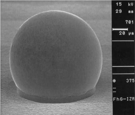
Eutectic solder bumping has meanwhile been developed with high connection density down to pitches of 25 m [79] and bump dimensions of (15 m)3. High yield is obtained with Sn/Pb as well as with lead free Sn/Ag or Au/Sn alloys [80]. The ultimate pitch limit is believed to be around 5–10 m [25]. Readout ICs typically have Al or Cu pads for bump connection bounded by a passivation layer for chip protection. Typically a thin (100 nm) Ti:W layer is first sputtered onto the wafers to promote adhesion and provide a barrier to prevent Cu atoms from diffusing into the pad metal (Al). Then a Cu or Au plating base ( 150 nm) is applied for the electrochemical contact followed by a well wettable Cu layer (1–5m). This layer stack is the UBM and is applied to both mating parts. In a wafer-based process cylinders of an electrodeposit are now grown onto the UBM of one part and turned into a spherical shape by reflow. Bonding of both parts is so far mostly done after dicing of bumped readout ICs and sensor plates or wafers supplied with UBM in a flip-chipping process and subsequent re-melting of the solder bumps. Note that this reflow process provides self-alignment of the mated parts.
Eutectic solder bumping is regarded as present day’s workhorse bonding technique for hybrid pixel detectors. For the ATLAS pixel detector very high bond yields of more than 99% have been obtained (i.e. number of modules not rejected due to bonding issues).
In-In bonding
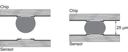
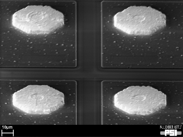
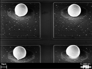
In-In bonding has also been used in LHC pixel detectors for a large quantity of pixel modules. The technique usually employs vapour deposition666electroplating of indium is also possible of indium through openings in the lift-off masks deposited on the wafer (see e.g. [1]). The mask is pulled off from the wafer by a wet lift-off process, requiring the bumps to be fairly flat and thin (10 m, fig. 14(a)). Also a UBM is necessary for this process, usually Ti-Pt-(Au) is used. The applied indium bumps are then bonded by thermocompression at about 100 ∘C. The advantages of the technique are its ease of application and the low temperature requirements. The bonds are, however, comparatively fragile, and the fabricated modules tend to have a lower mechanical damage threshold than solder bumped assemblies. In the Run-1 ATLAS pixel detector about 50% of the modules were produced using In-In bonding, showing high reliability with acceptance yields around 90. For the CMS pixel detector a reflow step has been introduced after bump deposition [81], turning the In bumps into spherical shapes (fig. 14(b)). The two spheres are merged in a second reflow at 180 ∘C. This provides a larger distance between chip and sensor, but it introduces self-alignment and stronger bonds.
Adhesive bonding
Recently adhesive wafer-to-wafer bonding has been discussed in the context of active CMOS sensors, capacitively coupled to readout chips where the capacitive coupling is provided between the metal pads of sensor and chip, respectively, separated by the adhesive bonding layer. Adhesive bonding has been claimed to reduce production cost by avoiding the UBM, bump deposition, and reflow steps. This has, however, not yet been demonstrated and is not at all obvious. Planarity requirements are stricter and requirements for alignment for chip-to-chip/sensor placement are the same as for standard bump bonding, the latter being the cost driver, not to mention the need for (cost intensive) electrical connections of the mated parts if provided by TSVs.
In the context of capacitive coupling of 'smart sensors' to readout ICs (CCPD) adhesive bonding has been investigated regarding thickness control and uniformity of the adhesive as well as radiation tolerance [82]. Good glue uniformity at the micrometer level has been achieved, however further evaluation of its competitiveness is needed, in particular whether electrical connections can be provided by cheap techniques like e.g. wire bonding, thus, however, abandoning the goal of compact module shapes.
Cu-Cu direct bonding
Metal-metal adhesion (Cu-Cu or Au-Au) of flat and polished surfaces has been known for a long time. The bonding forces principally involve capillary, Van der Waals, and electrostatic forces, as well as solid bridges caused by impurities and hydrogen bonds between OH groups.
Two mirror-polished wafers are put into contact and held together by adhesive forces without any intermediate material [75]. The process completes by Cu atom diffusion between the two Cu layers. Thermocompression (diffusion) bonding is simplest, but the required temperatures are usually too high for typical sensors and CMOS chips used in pixel detector applications.
Especially interesting is surface-activated Cu-Cu bonding as it works at ambient temperature. Surface-activation in this context means increasing the bonding force by surface treatment, e.g. by augmenting the number of hydrogen bonds (hydrophilicity) or by generating new types of chemical bonds. The treatment methods comprise wet chemical processes and (oxygen) plasma etching. The bonds are electrically conductive, an advantage for any wafer-to-wafer but also chip-to-wafer bonding project.
Requirements for good bonding are native oxide and other remnant removal, excellent chemical-mechanical polishing (CMP), and highly planar parts (wafers) with sufficient total Cu fraction. Very fine pitch ( 4 m) and low capacitance contacts are possible. The demands on surface cleanliness and flatness are the biggest drawbacks. Wafers must be processed soon after fabrication. Wafers must be very planar and sufficiently stiff which might compromise very thin solutions. At present the technique is also still fairly expensive.
Oxide-oxide direct bonding
Under room temperature conditions silicon wafers are covered with an oxide layer that can be used for direct wafer bonding, a method commonly used for SOI wafer production. Most common is 'hydrophilic' wafer bonding in which the wafers are, after cleaning, rinsed or stored in deionized water. Water is bonded via Si-OH groups on the silica surface. The bonding can be done at room temperature but the bonding strength increases with temperature (and time). With the addition of an electric field one speaks of anodic bonding, which can tolerate rougher surfaces.
Required is high quality CMP polishing and extremely good surface cleaning to avoid large bonding voids. The bonds are non-electrical. Hence TSVs or other electrical connections are needed for pixel assemblies. For this process wafer-to-wafer bonding is much easier than chip-to-wafer or chip-to-chip.
Solid-liquid interdiffusion bonding (SLID)
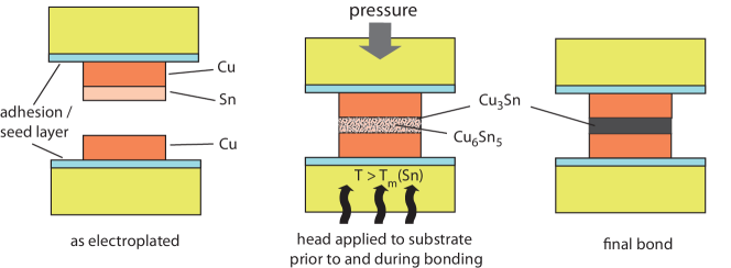
SLID bonding uses an intermetallic alloy formation and represents an alternative fine-pitch bonding technique based on thin (often eutectic) Cu-Sn connects [83, 75]. Between two Cu layers of several micron thickness a thin (3 m) Sn layer is applied on one of the Cu layers (fig. 15). They are brought in contact and heated to a temperature of around 240–320 ∘C. At this temperature the tin diffuses into the copper forming the Cu-Sn alloy. As the melting point of this alloy is around 600 ∘C multiple layers can be stacked and connected without melting the previously formed SLID connections. Furthermore, the process is also a flux-free bonding alternative with pitches much below 20 m, whereas the number of processing steps is about the same as for solder bonding (the reflow step is not needed). Technically, for SLID, pressure and temperature are required during the bonding step. This renders sequential bonding of multi-chip pixel modules necessary (chip after chip), whereas bonding by reflow does not require pressure (c.f. page 3.3) and can be done in parallel for a number of chips bonded to a sensor plate.
Despite their similarity SLID and soldering are fundamentally different processes with distinct and unique properties. A major difference is that soldering is reversible, whereas SLID is irreversible and only melts at temperatures much higher than the SLID process temperature. This implies also that no reworking is possible. Some process similarities to metal-metal thermocompression bonding also exist. A detailed comparison is given in [75]. SLID is particularly suited for wafer-to-wafer and chip-to-wafer bonding.
3.4 Wafer thinning
Thin wafers are a goal not only for low-mass pixel detectors in particle detection, but also for a number of integration processes, in particular for Through-Silicon Vias. While thick wafers are better for handling, other process steps like for example etching benefit from small wafer thickness. However, dedicated 'handling wafers' are needed to deal with flatness and bowing issues. Often handling wafers are of the SOI (Silicon-on-Insulator) type, because the Si-SiO2 interface transition offers a sharp etch stop with the oxide also acting as a sacrificial layer after ion etching.
Wafers are thinned by (backside) grinding. The active (front) side is first protected by tape. Grinding in two steps (coarse/fine) is performed using grinding wheels with diamond grain sizes from 1-8 m (fine) to 20-80 m (coarse) diameter. After the thinning process, breaking strength, warpage, and bow are characterization parameters that depend on the grinding tool characteristics and the grinding speed. More details are given in [76].
3.5 3D-integration and through-silicon vias
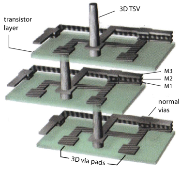
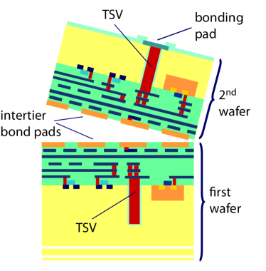
Extending electronics integration into the third dimension is - apart from feature size shrinking - regarded as the second route to ever increasing circuit density. 3D-stacking of several electronic device layers (tiers) is thus an eminent field of industrial research. Further advantages are reduced power consumption due to smaller connections and smaller involved capacitances as well as larger I/O bandwidth and more functionality at lower cost. Vertical vias running through layers of silicon (TSVs) are a key ingredient for 3D-stacking [76]. Tiers can be different CMOS layers but also electronics and sensor layers or layers interfacing to an optical signal transport. Figure 16(a) is a sketch illustrating the principle of 3D-interconnection via TSVs.
Besides TSV fabrication, wafer thinning and aligned wafer bonding are the key follow-up processes for 3D-integration. Direct bonding, especially Cu-Cu fusion or SLID (see above) are the preferred bonding techniques for 3D-stacking, providing strong fine-pitch bonds that are also conductive.
For future pixel detectors in particle physics, 3D-integration and TSVs are of interest if (a) wafer scale production becomes practical and/or (b) if TSVs allow better connectivity of detector modules by avoiding space consuming wire bonds and providing better buttable modules. In addition TSVs can reach through to the backside of a chip, allowing redistribution of electrical connections on the chip’s backside metal is addressed. This in turn saves the material normally added by flex interconnect circuits.
TSV fabrication
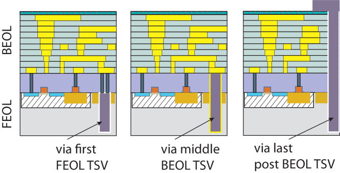
In IC fabrication all processes before the first wiring metal are called front end of line (FEOL), whereas the back end of line (BEOL) begins with this first metal processing and ends with the last IC processing step. Different types of TSVs are distinguished depending on the point in the process flow at which they are fabricated [87], i.e.
-
1.
via-first or FEOL via (polysilicon) applied before or during FEOL fabrication.
-
2.
via-middle or BEOL via (metal) applied after FEOL during BEOL fabrication
-
3.
via-last or post-BEOL via(metal) applied after IC fabrication post-BEOL. Here one distinguishes also front side via-last as in fig. 17 (right) and backside via-last, depending on whether the via is etched from the front through the BEOL stack (difficult) or from the back through (thinned) silicon substrate.
Note that the conducting material for FEOL TSVs must be doped polysilicon for reasons of thermal and material compatibility, having the disadvantage of higher resistivity compared to metals. For BEOL and post-BEOL vias tungsten and copper are most common. Figure 17 shows these distinct TSV types schematically.
Important TSV specifications are diameter, pitch, and aspect ratio (length-diameter ratio). Present typical ranges are given in table 2.
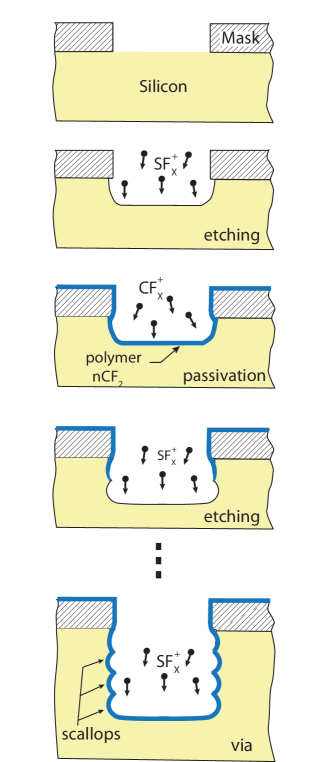
The main process for TSV production is deep reactive ion etching (DRIE, invented by Bosch [86]). The process employs a directional repetitive sequence of ion etching and wall passivation resulting in anisotropic etching of the silicon bulk. The principle is shown in fig. 18. The alternating cycles (typically lasting about 5 s) are: etching under a bias voltage with SF6 or NF3 in argon atmosphere to form gaseous SiF products - passivation of the surfaces with C3F6, C4F8, or CHF3 in argon forming a protecting fluorocarbon polymer surface layer on sidewalls and bottom. The bias voltage provides a directional orientation of the bombardment. The resulting via has a typical scalloped surface with undercuts that are, however, substantially reduced by advanced DRIE parameters.
First HEP experiences with TSVs
A characteristic of TSV application for HEP pixel detectors is the fact that readout chips or sensors are still comparatively thick (100-200 m) for via fabrication. On the other hand the required via pitch and density often is relaxed, for example when only service lines need to be via-connected or when I/O pads can have large pitches.
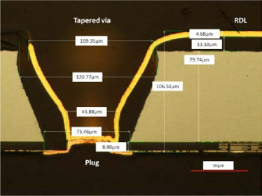
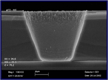
Therefore, the first successful HEP pixel module operation employing TSVs [89] was obtained with small aspect ratio (1:1) tapered vias as shown in fig. 19, fabricated at Fraunhofer IZM, Berlin. Chip wafers (FE-I3) of the ATLAS pixel detector production were thinned to about 80 m thickness. The I/O pads were accessed through TSVs and redistributed on the backside of the chip. The via geometry can be seen from fig. 19(a): 110/45 m diameters (top/bottom), tapering angle, 150 m via pitch. After wafer dicing a pixel module was assembled by bonding a readout chip containing vias to a pixel sensor using solder bonding. The pixel module was operated and characterized with radioactive sources without performance loss compared to modules connected via wire bonds instead of vias.
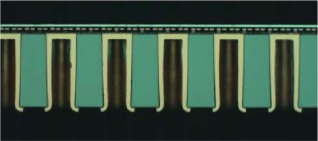
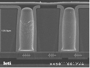
Larger via depths and aspect ratios are required to connect large area chips like the ATLAS FE-I4 chip [6] having about 22 cm2 area. Without handling supports, such chips show large bows and the thickness must be optimized for handling, bonding, and TSV yields. A successful approach was achieved using straight copper vias (Fraunhofer IZM, Berlin) with an aspect ratio of 2.7:1 applied to 160 m thick FE-I4 wafers [90],[91] (fig. 20(a)). Similar efforts are carried out at LETI/CEA [92] (fig. 20(b)). A 22 cm2 pixel module was produced along similar lines containing about 25 500 pixels, and characterized using radioactive sources. To increase the via yield to close to 100% a new approach using chip wafers thinner than 100m with handling wafer support using straight Cu-coated vias is under way.
4 Readout integrated circuits, data transmission, and power distribution
The ROIC provides the functionality of a hybrid pixel assembly. From the start, the purpose of the hybrid approach has been to allow independent optimization of ROIC and sensor [94]. The ROIC technology development has been enabled by Moore’s Law (the doubling of logic density every 2 years in commercial electronics) towards deep submicron commercial CMOS, in order to meet rate and radiation tolerance demands. The alternative of stacking circuit layers in the 3rd dimension without reducing feature size has also been explored, but has so far been less successful. Data transmission and power distribution are system challenges concerning the ROIC as well as other elements such as optical components, encoding/decoding protocols, cables, and cooling.
4.1 CMOS ROICs
It is useful to classify CMOS ROICs in terms of generations, which have a rough correlation with the feature size used. First generation pixel chips are typified by those in the original ATLAS and CMS detectors [95, 96], Medipix [97], using 0.25 m feature size CMOS with custom layout techniques for radiation tolerance. Second generation chips have been developed and fabricated using 130 nm CMOS and are running in current experiments or devices [6, 98, 99]. Third generation chips are under development, focusing on 65 nm CMOS [30, 100, 101]. Table 3 shows the evolution of memory and readout bandwidth between generations.
| gen. | gen. | gen. | |
|---|---|---|---|
| Hit data storage density | Gb/s/cm2 | 5 Gbps | 40 Gb/s/cm2 |
| Chip output bandwidth | 40-160 Mb/s | 0.3-1.2 Gbps | 2-20 Gb/s |
The basic elements and organization of a hybrid pixel readout chip are common to all generations and applications. The defining characteristic is the use of a dedicated amplification and discrimination channel per pixel (front end), with the ability for all these front ends to operate in parallel, followed by parallel processing of the output signals. Section 4.6 reviews the front end characteristics. The output of the front end is most commonly digitized in some way on the pixel, but can also be sampled on an analog memory for later readout as an analog level [96]. On-chip digitization allows for higher readout bandwidth with pure digital readout and is expected for all third generation chips. The preferred digitization method has so far been ToT (see section 4.6). We normally refer to a pixel firing when the amplified signal exceeds the discriminator threshold. Managing power transients and noise coupling when all pixels are simultaneously live (having the ability to fire at any time) is a main system challenge of pixel ROIC design. Many chips are designed for a given maximum occupancy (number of pixels firing at once) and therefore only guarantee system stability in applications that do not exceed this occupancy.
While the front end architecture remains similar from one generation to the next, processing of the information produced by the front end, and the relationship of the front end to the rest of the chip, have evolved significantly. First generation chips were mainly analog circuits, with some logic and memory to manage hit buffering and readout. The most salient new feature of second generation chips was the use of synthesized logic side-by-side with analog front ends in the entire pixel matrix, but with an organization in columns and small digital blocks stepped and repeated. The third generation will go further, implementing an almost entirely digital chip, with a large number of pixels within a synthesized logic basic unit. The front ends will be embedded as data sources within a digital fabric entirely surrounding each analog unit.
Logic density is critical to pixel ROIC design, unlike in most other physics detector applications, where analog performance tends to be of the highest importance. Achievable logic density is intimately tied to rate capability as will be seen later. The 1st generation chips had a mainly analog pixel matrix, with digital operations implemented using full custom circuits (produced with analog design methods). Any digital processing and data buffering were done in the periphery. This resulted in a relatively large periphery area and the need for high bandwidth data transfer from pixels to periphery (see section 4.7). The most prominent new development in 2nd generation chips was the use of synthesized logic within the pixel matrix, enabled by a leap in logic density (see section 4.3). Thus the matrix became a mix of analog columns designed with conventional analog methods and digital columns synthesized with digital design tools. Digital processing and storage in the columns meant the periphery area could shrink and the hit rate capability increased (section 4.7). The 3rd generation chips are now expected to be essentially digital, with embedded analog amplifiers kept to a minimum and logic complexity rivaling commercial microprocessors. This opens the door to unprecedented functionality within the front end chip.

A key element in the transition to essentially digital chips has been isolation of circuits within the same chip. Digital switching produces current spikes. Even if analog and digital circuits use different power supplies and grounds, return currents induced in the silicon substrate can inject parasitic signals into sensitive analog circuits. This can be mitigated by isolating circuits from the bulk substrate, using options provided in many deep submicron processes. Figure 21 compares schematically a logic inverter in conventional CMOS with the triple well version. It can be seen that the NMOS device and the local ground are isolated from the substrate in the triple well process. Some processes offer more sophisticated implant structures that allow further isolation of the N wells, involving separately biased additional wells and/or insulating trenches. Silicon on Insulator (SOI) processes have not been popular for high radiation tolerance because they contain a thick oxide layer under the circuitry that accumulates trapped charge with radiation dose, giving rise to undesirable back-gating effects in fully depleted devices (FDSOI). The format of isolation structures exploited varies with vendor and technology. Designs also vary between isolating only analog circuits, only digital circuits, or both from the true bulk substrate. While such isolation strongly attenuates noise coupling, it does not completely eliminate it. Therefore, in addition to isolation, controlling power consumption transients or changes during chip operation is increasingly important. Isolation implants have also been exploited for monolithic active pixel designs, covered in chapter 6.
Logic density is most important in a triggered system (see section 4.7). This is the case for the highest rate detectors in a collider geometry, where the raw hit volume is too high to allow for read-all operation with an acceptable mass of data cables. In a triggered system the ROIC function is to remember the position, arrival time, and charge of all hits until a trigger arrives. The rate of hits depends on the rate of particles impinging on the detector and, since each hit requires a certain number of bits for digital storage, it can be characterized as a specific bandwidth in bits per second per unit area, as was done in table 3. Note that this does not depend on pixel size to first order, but on particle flux (one incident particle makes one pixel cluster regardless of pixel size, and with the use of region architectures (section 4.7) the effect of cluster size is small). Given a particle flux, the total memory needed depends on the trigger latency, which is typically a few microseconds. The achievable memory per unit area is limited by the CMOS process logic density. Thus, for a triggered system, higher hit rate (and/or longer latency) requires higher logic density. This requirement, not pixel size or radiation, has driven pixel ROICs for high rate and radiation to ever deeper submicron CMOS processes (e.g. 65 nm instead of 130 nm). This is not immediately evident, because pixel size also scales down with increasing hit rate. However, simply making smaller pixels would not require a new process with smaller transistors (smaller feature size), since the analog functionality uses a small number of relatively large transistors. The requirement that does demand smaller transistors is increased logic density. The reason pixel size must also be reduced with increasing hit rate is to avoid in-pixel pileup. After registering a hit, a pixel needs a certain recovery time before being able to record another hit. To avoid losing efficiency to in-pixel pileup, the average time between hits in any given pixel (which scales inversely with pixel area) has to be much longer than the recovery time. An alternative solution is synchronous operation (where every pixel resets before each beam collision). This has been investigated, but so far it has not been popular because, as such a front end must be faster, it consumes more power.
4.2 Increasing circuit density through 3D integration
The use of TSVs in hybrid assemblies has been discussed in section 3.5 in the context of assembly integration. Very small TSVs can also provide an alternate path to increase logic density (in a given footprint) by stacking and vertically interconnecting multiple tiers of circuitry. Stacking of circuit layers this way results in a linear increase in logic density with number of layers, whereas feature size reduction results to first order in a quadratic increase with feature reduction factor. In the commercial sector, industry has so far preferred Moore’s Law scaling over 3D integration. Only for future system-on-chip architectures, below the 10 nm feature size or equivalent, do industry leaders favor 3D integration [102]. One big advantage of 3D integration is reduction of power. This is because power scales with distance between switching elements, and in 3 dimensions more switching elements can be placed in close proximity than in 2 dimensions. In fact, the main actual and growing use of 3D integration in commodity complex devices is to put memory as close as possible to processors, by integrating a 3D memory stack directly on top of a CPU chip [103]. This increases transfer speed and reduces power. But since high volume introduction of TSV in 2006, the fastest growth of 3D integration has been in DRAM memory and image sensors, where either simple and regular structures (DRAM) or heterogeneous structures (image sensors) are being stacked. The solid state RAM use case is obvious: it is not an alternative to Moore’s Law scaling, but an augmentation of it. The DRAM levels being stacked already have the highest available 2D logic density and 3D integration is the only way to fit even more into a given footprint. In High Energy Physics, the use of 3D integration for higher logic density ROIC fabrication was explored (with 130 nm feature size CMOS), in parallel to the exploration of plain (not 3D) 65 nm feature size. Working devices were produced and good results were obtained [104, 105], but so far, as in industry, going to a smaller feature size process has been the more effective path to high logic density.
4.3 Radiation tolerance of readout integrated circuits
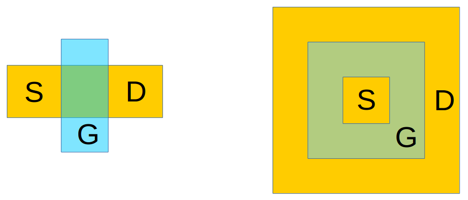
First generation radiation hard ROICs were only possible in commercial 0.25 m CMOS processes with custom enclosed layout transistors (ELT). They achieved radiation tolerance above 50 Mrad [106]. In an ELT the gate completely surrounds the source (drain) and in turn the drain (source) surrounds the gate (fig. 22). This avoids some channel edge effects (discussed later) since the channel is edgeless, but uses more real estate than a traditional linear transistor. ELT in 0.25 m CMOS represented a 2.5-fold increase in logic density over 0.8 m feature size military grade radiation hard technology used in the 1990’s, and this enabled sufficient logic density to produce the triggered ROICs for ATLAS and CMS. Early development of pixel ROICs using 0.8 m radiation hard processes did not succeed in incorporating all the needed functionality in a uniform pixel matrix; the logic density was simply not high enough. Because of the ELT area penalty, radiation hard 0.25 m lagged behind the Moore’s Law scaling of their commercial counterparts (fig. 23). Starting with the 130 nm node, the minimum size linear transistor standard cell logic used commercially exhibited high total dose radiation tolerance. The ability to use linear transistors translated into a faster than Moore’s Law increase in radiation hard logic density, which went hand-in-hand with the transition to generation chips with synthesized logic in the pixel matrix. In addition to high logic density, the good performance of linear transistors enabled the out-of-the-box use of commercial logic libraries. These have been perfected and extensively validated by large scale commercial manufacturers of consumer electronics and come well integrated with powerful design and simulation tools. However, the use of linear transistors comes with some risks and side effects, which, once again, make radiation hard circuits in 65 nm lag their commercial counterparts in logic density.
The radiation hard design approach of and 2nd generation ROICs was to make or find devices (transistors) that tolerate the required dose without significantly changing their response. The design process typically included increased margin on the specifications, but otherwise relied on the device models available from the manufacturer. After fabrication, the ROIC was tested to measure the actual radiation tolerance. This approach is still followed for analog circuits. Optimization of analog performance would suffer if one had to consider a wide range of properties for each transistor in the circuit, so working with fixed properties is desirable. Fortunately, since for analog circuits the transistor dimensions and geometry are fully under the designer’s control, it is possible to choose transistors that suffer little change with radiation, which means larger than minimum dimensions in the case of deep submicron CMOS (section 4.4).
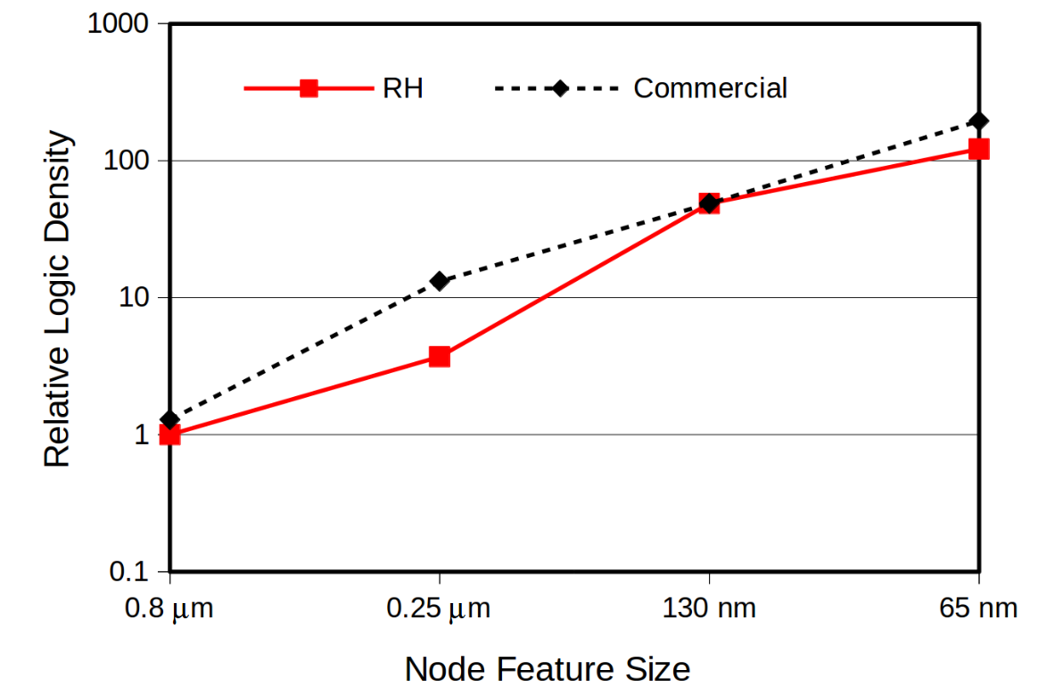
On the other hand, for high density synthesized logic designers do not have the freedom to select devices that show little change with radiation. Instead, digital design must increasingly rely on accurate modeling of radiation damaged transistors. Conventional digital design already offers several different models for the same transistor: a typical model plus so called corner models, which simulate operation with different temperatures, voltages, and/or variation of fabrication process parameters within an allowed range. The same transistor will be faster or slower depending on temperature, and so on. The synthesis tools produce circuits to function in all the selected corners. The new design approach is to use additional corner models that represent the radiation damaged transistors. Such models can be custom made by parameterizing measurement data. In this way, logic can be synthesized to work both before and after radiation damage, even though logic gate propagation delays, setup and hold times, etc. can change very significantly: a factor of 2 or more. This is to be compared to changes of just tens of percent between the operating temperature extremes. Such large changes will limit the achievable clock speed, but most pixel ROIC applications require clocks of order 100 MHz, rather than the typical GHz speeds of microprocessors in the same technology. Radiation damaged transistor models are also used to simulate analog and mixed signal circuits in order to confirm the design prior to fabrication and radiation testing, which still provides the ultimate validation.
4.4 Total dose radiation damage in CMOS transistors
Radiation damage in CMOS circuits is entirely due to charge carriers generated by ionization in the dielectric layers of the process, and not to bulk damage of the silicon lattice. Ionizing dose is delivered at hadron colliders by a combination of minimum ionizing particles (mainly pions) and background X-rays. The doping concentrations in CMOS transistors are high ( cm-3 and higher), compared to which the defect density introduced by bulk radiation damage is negligible [107] (below cm-3 for HL-LHC inner layers after 3000 fb-1). However, there are many dielectric structures in a modern CMOS process and each one leads to its own radiation effect due to ionizing dose. It is not by accident that radiation tolerance requirements have kept pace with the logic density evolution in the ROIC generations. The reason is that both hit rate and radiation dose scale with particle flux. Required radiation tolerance went from 50 Mrad for the generation, to 250 Mrad for the , to 1 Grad in the . 1 Grad corresponds to about 50 minimum ionizing particles crossing every Si lattice cell. Not all effects from charge generation in the dielectrics are equally important. As radiation dose increases, understanding and managing previously negligible effects becomes necessary. The importance of each effect also depends on transistor geometry and size. In this respect, the 130 nm CMOS technology node represented a 'sweet spot' for which commercial logic libraries could be used out-of-the-box up to doses well in excess of the Mrad requirement (double or perhaps triple). In contrast, in the 65 nm node it is necessary to select or customize logic cell designs depending on the desired radiation tolerance, effectively trading off radiation tolerance for logic density. If the expected radiation dose is low, the out-of-the-box commercial logic can be used, while for higher expected doses, lower density logic cells must be substituted (The logic density point shown for 65 nm in fig. 23 was appropriate for an expected dose of 500 Mrad). These general statements should be seen as rough trends, and must be tempered by process specificity and environmental effects discussed later. Beyond 65 nm, which is at present well characterized, new research in high energy physics instrumentation is focused on understanding radiation damage in 40 nm and 28 nm feature processes [108], with detailed investigations expected over the coming years.
Oxide charge and its effects
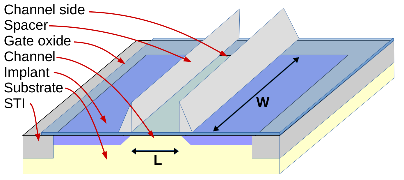
Three oxide structures have been identified as producing radiation damage effects in the bulk CMOS processes used so far: the gate oxide, the shallow trench isolation oxide (STI), and the gate spacers, all shown in fig 24. Ionizing radiation generates charge carriers within these oxides, which can lead to an accumulation of positive static charge, because hole mobility in SiO2 is 6 orders of magnitude lower than electron mobility. While charge in the gate dielectric would be most problematic, because it would directly cause a threshold shift, gate oxide in 0.25 m feature size and below cannot charge up. The gate oxides are thin enough (6 nm and below) that quantum mechanical tunneling is an important effect, resulting in an effective electrical conductivity. Tunneling also means that there is a gate leakage DC current (unrelated to radiation), which is what eventually caused industry to move away from silicon dioxide gates in nodes below 45 nm feature size. The gate leakage in the nodes used so far for pixel chips is not yet large enough to result in significant standing power consumption, but it is visible in bias networks, which are high impedance nodes feeding large gate areas.
STI and spacers are both thick oxide structures and therefore will accumulate positive static charge. However, not all the positive charge is truly static. Charge held in so-called deep traps is static at normal temperatures, but charge in shallow traps will gradually drift in an applied electric field (as present during chip operation) and will thus reach the oxide-silicon interface. This is a complex region which undergoes manipulation during the fabrication process [109]. This manipulation involves the passivation of so-called dangling bonds, which would otherwise manifest themselves as states within the energy band gap and spoil the semiconductor properties. Positive charge reaching the interface reverses some of the passivation, bringing back some of the traps that were painstakingly neutralized during fabrication. However, these will then trap negative charge, and that will actually compensate some of the oxide static charge. Remarkably, we would not be able to use commercial CMOS processes for ROICs, were it not for this fortunate cancellation of two detrimental phenomena: oxide charge and interface traps.
At relatively low dose (up to a few Mrad) the net results can be complex depending on the time constants for positive charge drift, the activation of interface traps, and their subsequent trapping of negative charge. These time constants can be vendor-specific, depending on oxide structure formation chemistry and steps, and are certainly affected by temperature. At high total dose the movement of charge and activation of traps have equilibrated, leading to an approximate, but not perfect cancellation of interface charge. A positive net charge always remains, and this degrades transistor performance. Since the sign of this net charge at the oxide-silicon interface is always positive, it affects NMOS and PMOS transistors differently. The net positive interface charge results in parasitic lateral gating in the case of STI and in a modification of source and drain in the case of spacers. The former is known as Radiation Induced Narrow Channel Effect (RINCE) [110], while the latter is known as Radiation Induced Short Channel Effect (RISCE) [111].
RINCE
RINCE or lateral gating affects the sides of the channel (see fig. 24), causing them to be conductive in the case of an N-channel and non-conductive in the case of a P-channel. This does not have a significant impact on a wide transistor, because a small fraction of the total current flows near the sides. But in a very narrow transistor all the current is near the sides and the effect can be large, hence it is called Narrow Channel Effect. ELT’s were used in 1st generation ROICs to avoid this effect, as the channel in an ELT has no sides (fig. 22). This was necessary in 0.25 m technology, because the radiation-induced parasitic standing current in linear NMOS transistors was measured to be too high for a useful design. But note that, while an ELT has no sides, it also cannot have a very narrow channel. The width of the channel must be at least the perimeter of the source or drain, and so has to be many times the minimum feature size. Therefore, as long as standing parasitic current is tolerable, making wide conventional transistors is just as good as making ELT’s, with the advantage that conventional transistors are standard and extremely well modeled. Thus, in 130 nm and below, ELT’s have not been used. This led to some surprises at low total dose in the case of the ATLAS IBL detector [112]. The parasitic standing current in NMOS transistors, while completely tolerable at high radiation dose, can go through a transient period of being higher than tolerable depending on vendor and on temperature. Accurate modeling of this varying leakage current behavior has been now developed [113].
RINCE affects PMOS and NMOS transistors in opposite ways. NMOS transistors develop parasitic standing current, but this does not interfere with the transistor action, it simply adds to it. PMOS transistors are parasitically turned off near the sides, which hinders the transistor action. A critical question for PMOS is how far away from the sides is the channel affected by interface charge. The effect can be visualized as a radiation dependent width change, such that the effective width is , where is the width as drawn, is how far away from the STI-channel interface is the channel affected, and TID is Total Ionizing Dose. From the observation that minimum width PMOS devices in 65 nm feature size are highly degraded at 500 Mrad, while those in 130 nm feature size are mildly degraded, we can say that (500 Mrad) 30 nm.
RISCE
RISCE affects PMOS and NMOS in a similar way, by impeding charge flow between source or drain and channel. It can be roughly modeled as 'adding' a certain length to the channel (a longer transistor conducts less current than a shorter one). One may therefore think that making very short transistors would be a good strategy against RISCE, because this would be a way to compensate. But the opposite is true: longer transistors are less affected by RISCE, because the relative change in effective length is small if the original device is long to begin with. Once again we can write , where we are now adding effective length rather than subtracting effective width. The magnitude of the effect is about twice as large in PMOS than in NMOS. A 60 nm long PMOS (NMOS) will experience a 70% (30%) reduction in full-on current after 500 Mrad. Since transconductance scales as , a 70% (30%) reduction in current is equivalent to a factor of 2.5 (1.4) increase in length. For the original channel length of 60 nm this implies (500 Mrad)45 nm (12 nm) for PMOS (NMOS).
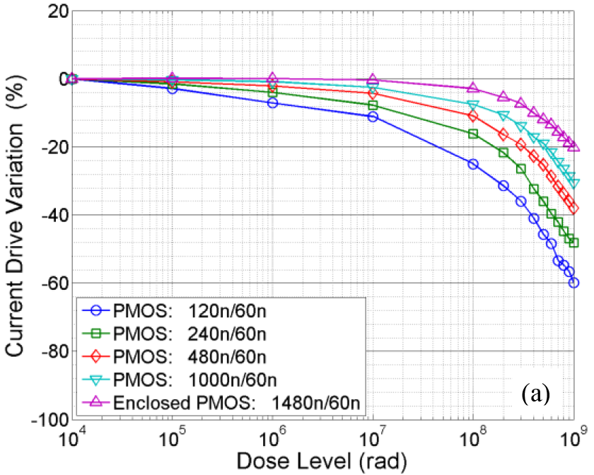
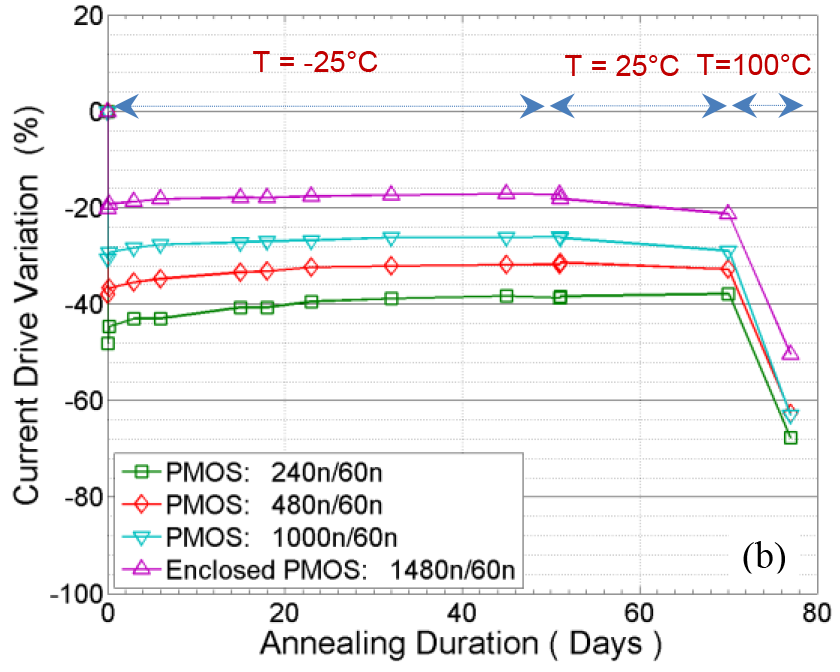
Dependence on voltage and temperature
The above (500 Mrad) and (500 Mrad) should be seen as rough sketches of a more complex underlying behavior, and were given to provide intuition about the magnitude and sense in which the transistors are affected, and why the effects become more important with decreasing feature size: effective width and length should not be regarded as a real model.
The RINCE and RISCE effects are modulated by transistor bias and by temperature. In general, both effects occur only when transistors are powered, which means there are electric fields in the STI and spacer oxides. The larger the field (which depends on transistor bias conditions) the greater the effect, though there are quantitative differences between NMOS and PMOS. The effective width and length given above are for worst case bias. Unpowered devices suffer little or no damage regardless of temperature - an important point to keep in mind when estimating how long a detector will last.
For powered devices, high temperature increases damage during irradiation, and can decrease (anneal) or increase damage after irradiation. Figure 25 shows results of a study [114] in which different width PMOS devices were first irradiated at low temperature and then annealed at different temperatures, always under power. All transistors are minimum length. When powered, devices can suffer very large damage in a matter of hours at 100∘C, but the same damage at 0∘C would take over 10 years. This suggests that activation of deep traps is responsible. As an oxide can contain multiple traps with different activation energies, the effect can be complex and process-dependent, which is confirmed by observations. Since the combination of power and high temperature is explicitly excluded by interlocks in all pixel detectors, the main impact of high temperature annealing damage is to complicate qualification. The high integrated dose on a detector is delivered gradually over years. Past qualification protocols emulated this with high dose rate irradiation followed by high temperature annealing. However, application of such protocols is no longer straightforward in 65 nm. Activation energies must be precisely determined before thermal acceleration tests can be confidently applied.
4.5 Single event upsets and mitigation
In addition to long term degradation due to accumulated dose, energy loss by ionizing particles leads to instantaneous soft errors called Single Event Upsets (SEU). The most common SEU is the flipping of a stored bit in a memory. SEU also can produce voltage transients on signal or control lines that can result in accidental operations - for example a single level asynchronous line to reset logic or memory would be vulnerable to SEU. Protection against SEU involves hardening of memory cells, avoiding designs with vulnerable control signals or hardening control signals where their use cannot be avoided, and circuit triplication. These techniques have been in use since 1st generation ROICs and have not seen significant changes in the 2nd generation. However, as collider rate continues to increase and higher logic density translates into lower deposited charge needed for upset, these techniques will no longer be sufficient. An approach being introduced in 3rd generation ROICs is to design for reliable operation while a significant level of upsets is taking place. Fundamentally this is abandoning the idea of circuit hardening as a solution to the SEU problem, and instead designing all functions such that SEU is not a problem to begin with. In practice, a combination of hardening and SEU-friendly functionality will be used.
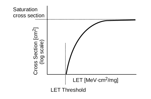
Extensive literature and experience exist on SEU of memory cells in the context of electronics used in space. This is not directly applicable to particle physics pixel detectors, but nevertheless a good starting point. SEU of a given circuit, like an SRAM cell, latch, or flip-flop, depends on the amount of energy deposited by an impinging ion, which is characterized by a Linear Energy Transfer (LET). It is important that this is meant to describe non-relativistic ions, which lose energy approximately uniformly along their path through electromagnetic interactions. The upset rate is characterized by the cross section for causing a bit flip (SEU cross section). Cross section vs. LET is typically fit with a Weibull function, resulting in a threshold and saturation cross section as shown in fig. 26. In submicron technologies, the typical LET threshold pretty much regardless of memory cell type is of order 1 MeVcm2/mg. Saturation cross section varies with cell design, but is of order to cm2 for common SRAM, latches and flip-flops. However, an energetic proton (or pion) has a LET of order 0.01 MeVcm2/mg, which immediately signals that it cannot upset memory cells by the same energy loss mechanism as ions (it is far below the LET threshold). Upsets in this case are due to nuclear interactions. This can be seen from the fact that SEU cross sections are about the same for energetic neutrons and protons [115]. There is thus a kinematic threshold depending on the nuclei in the material, rather than a LET threshold. Typical SEU cross sections for protons are of order cm2 [115]. At relatively low energies, an adequate model has the proton imparting momentum to a nucleus which then becomes a traditional high LET heavy ion. But at the GeV energies of the LHC, inelastic collisions can produce showers of high LET particles affecting a large area of silicon. This is important for hardening techniques.
SEU hardening of memory cells exploits redundant connections or storage separated by some distance. This is more effective for heavy ions, which deposit energy very locally, but still useful for relativistic protons (or pions) which can produce extended deposits [116]. A type of memory called Dual Interlocked CEll (DICE) [117] is extensively used as its state can only be changed by switching two physically separate voltages in coincidence, which gives it a lower SEU cross section than common latches. Special layout techniques, such as interleaving can be used to carefully separate sensitive elements and prevent charge sharing [118]. Table 4 compares the SEU cross sections of common structures [119] in a high energy proton beam, for 65 nm technology.
| Cell type | Cross section in cm2 |
|---|---|
| Standard latch | |
| DICE latch with interleaved layout | |
| TR standard Latch | |
| TRL with error correction and control triplication | |
| TRL with error correction, control triplication | |
| and separation of sensitive nodes |
One is not always free to choose the memory type with the lowest SEU cross section. The almost 4 orders of magnitude gain from a standard latch to maximal use of triple redundancy in table 4 comes with an associated footprint increase of a factor of 10. Such cells can therefore not be used in the high density logic of the pixel matrix. Suppose every pixel has 8 bits of configuration and the acceptable fraction of corrupted pixels during an 8 h data run is 1%, with 1 GHz/cm2 particle flux. The run-integrated fluence is cm-2 and therefore the pixel SEU cross section must be 1%/( cm-2) or less. As there are 8 bits per pixel, the single bit cross section must be cm2 or less. Even without considering added design margin, tab. 4 shows that this requires triple redundancy, which may not fit due to its large footprint. A new solution to this problem in 3rd generation ROICs is to implement a control protocol that allows continuous writing of configuration data during data taking, instead of configuring in a distinct operation mode. If configuration values are constantly being refreshed from outside, one does not need to rely on 'long term memory' within the chip. For example if the time between consecutive writes is 1 s instead of the duration of the data run. this relaxes the SEU cross section requirement by 4 orders of magnitude. It should be noted that hit data have never required SEU protection, because the time that data bits spend in chip memory before readout is very short, given by the trigger latency. Thus the relevant time scale for hit data is of order 10 s for triggered, 3rd generation ROICs. Even with a significant error amplification from data encoding777For example, a single bit flip corrupts and entire 64 bit packet, the fraction of data lost due to SEU will be negligible with storage in standard latches888Since no detector is 100% efficient, data losses well below the 1% level are insignificant..
4.6 Analog front end and ADC
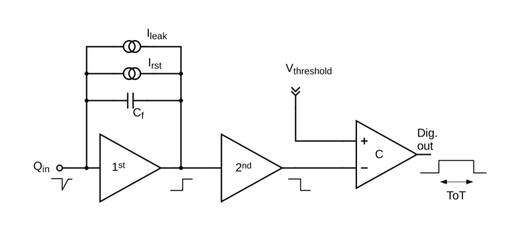
The analog front end elements are shown schematically in fig. 27. The front end design has universally consisted of a Charge Sensitive Amplifier (CSA), followed by a 2nd stage to provide additional voltage gain, and a comparator (C) to carry out the pulse height discrimination. The CSA has a 1st stage amplifier with capacitive feedback (Cf), a continuous reset (Irst) and a low bandwidth feedback to compensate for sensor DC leakage current (Ileak). This is needed because hybrid pixels have so far been DC coupled to the readout and sensor leakage current can be significant after irradiation (for development of AC-coupled pixels see section 3.1).
On-chip signal amplitude digitization has used ToT of the comparator output. ToT is a simple digitization method that counts clock cycles while the comparator is high (meaning above threshold). The most important function of the pixel front end has been to discriminate true hits from noise with the correct timing to within one bunch crossing of the accelerator, which for the LHC means 25 ns. This requires a fast leading edge response (high slew rate), which can be achieved with high input gain. The input charge to output voltage gain is given by the inverse of the feedback capacitor Cf in fig. 27 and the characteristics of the first stage amplifier. On the other hand, the charge transfer efficiency from the sensor to the integrator is given by (Cdet + Cf)/Cdet, where Cdet is the detector load capacitance and is the 1st stage open loop gain. Clearly, a high open loop gain is needed in order to have both high gain (small Cf) and good charge transfer efficiency. However, the specific transconductance (g, were is the drain current) of CMOS transistors is only of order 10 S/A, which means that a simple (i.e. single transistor) inverting amplifier can only achieve for 1 A current and 1 V supply, since g, where is the supply voltage. Two simple amplifiers in series would achieve an open loop gain proportional to g (so ), but with low bandwidth. The solution in pixel ROICs has always been to use a cascode topology for the 1st stage, which achieves an open loop gain proportional to gm(M1) gm(M3) without sacrificing bandwidth. The labels M1 and M3 refer to fig. 28, where two cascode variants are shown. In the straight cascode configuration (a), the current source M4 is larger than the current source M2, and their combined current passes through the input transistor M1. A small change in the input will cause a change in the M1 drain voltage according to the transistor’s gain. This in turn shifts the source of M3, leading to a significant Vgs change for M3, which amplifies the change in the output voltage. The M3 gate voltage is held at a fixed bias, Vcasc. In contrast, in the regulated cascode (b), the current source M4 is smaller than the current source M5, and the additional transistor M2 shifts the M3 gate voltage in response to a change of M1 drain voltage, leading to additional output gain (bigger Vgs change for M3).
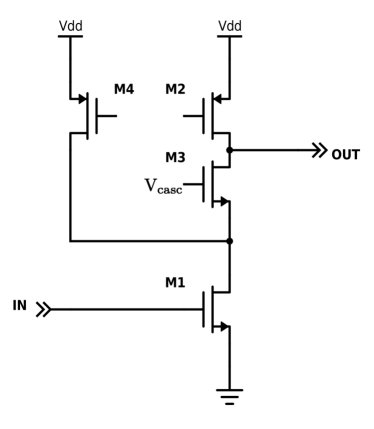
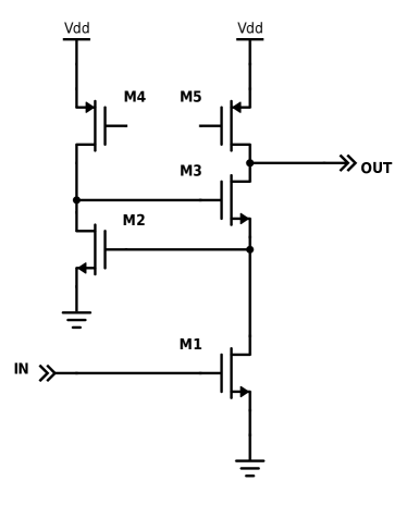
While the front end configuration and 1st stage cascode architectures have remained, there have been important quantitative changes between 1st and 3rd generation ROICs. The specific transconductance of CMOS transistors has nearly doubled going from 16 S/A in the 0.25 m process to 22 S/A in 130 nm to 28 S/A in 65 nm. The higher hit rate requirements have led to smaller pixels (with lower capacitance per pixel) and faster shaping to avoid in-pixel pileup. While some 1st generation ROICs used PMOS input transistors for better substrate isolation and better 1/f noise performance, with the faster pulse shaping and common substrate isolation techniques, NMOS has become the input device of choice for amplifiers in 130 nm CMOS and below [120]. The decrease in pixel capacitance (by about a factor of 4) and increase in transconductance have translated into higher gain and speed. The effect of time-walk is therefore significantly reduced in 3rd generation ROICs, even before making use of digital processing to correct the time of hits near threshold999Time-walk is the variation in relative delay between front input pulse and comparator firing, as a function of pulse amplitude above threshold.. While so far all detectors have used ROICs with continuous reset as shown in fig. 27, there has also been R&D on front end designs that reset before every bunch crossing (these are referred to as synchronous front ends) [121]. In this case there is by construction no time-walk, but the power consumption is higher due to the fast shaping and reset settling needed. So far this approach has not been adopted for pixel detectors.
The need for very high speed front ends with sub-ns time stamp resolution capability has been spearheaded by NA62 and its Gigatracker detector. The Gigatracker ROIC [122], implemented in 130 nm CMOS, uses a straight cascode front end with RC feedback. The RC time constant is 5 ns, which gives the device its 5 ns peaking time. Two differential gain stages are then used in front of a constant fraction discriminator to achieve a 200 ps time stamp resolution. Future fast timing detectors discussed in section 2.3 will continue to push this type of design to finer time resolution.
A pixel ROIC with free-running front ends is an inherently metastable circuit. Every pixel can fire at any time, and the act of firing switches logic that would not otherwise switch. Any coupling from digital switching to analog front end can be a positive feedback mechanism. For low enough threshold and/or enough pixels firing at the same time, this positive feedback can set off a chain reaction causing all pixels to fire. For a given instantaneous hit occupancy (fraction of pixels firing at the same time due to an external stimulus), there will be a minimum stable threshold. Each ROIC is different in this respect, but in general the minimum stable threshold was around 2500 electrons (e-) in 1st generation ROICs, whereas it will be around 500 e- for the 3rd generation. This reduction has been deliberate: required by decreasing input signal values. Large pixels ( m2), thick sensors ( m), and moderate sensor radiation damage for 1st generation detectors translated into expected signals of order 10 ke-, while small pixels ( m2), thinner sensors (100 m), and heavier sensor radiation damage will lead to signals as low as 2 ke- at the HL-LHC. The minimum stable threshold is reduced by exactly the same factor, since the important figure of merit for pixel detectors is not signal to noise ratio, but rather signal to threshold ratio. The front end noise does set a lower bound to the threshold, but does not determine how far above this lower bound is the minimum stable threshold. Assuming a noise occupancy of 10-4 is acceptable, this corresponds to the Gaussian 1-sided tail fraction for . Inverting the question, for a 500 e- minimum threshold, the noise must be less than 500/3.7=135 e- equivalent input charge. But this is just an upper bound. How far below this bound the noise needs to be depends on how the threshold varies with time and how from pixel to pixel.
One can express the front end noise requirement as
| (14) |
where ENC is the equivalent input charge noise, is the threshold, and is the threshold variation as a function of position () or time (). , or the pixel to pixel threshold variation, is known as dispersion. The main cause of dispersion is fabrication process mismatch between transistors and passives of identical design. While the mismatch amount is process dependent, and the translation from mismatch to dispersion is design dependent, a typical dispersion value is in the range of 300-500 e-. As this is clearly unacceptable, all ROICs so far have compensated for mismatch by programming a different threshold voltage in each pixel, such that in units of input charge all pixels have an equalized (or tuned) threshold value. With such tuning, a value of 40 e- dispersion is typically achieved. The cost of this technique is circuit area in the pixel in order to implement the needed DAC and memory. However, tuning only controls , and not . The main source of has been coupling of transients from other circuits to the front end, which has in turn been the main limitation on minimum stable threshold. This has been mitigated with circuit isolation, and control of power transients, as already explained. Still other sources of may gain importance in the future. In particular, short term radiation damage can spoil tuning and cause threshold shifts [123]. If the radiation dose in between tuning cycles is high enough, could become dominant for reasons unrelated to circuit isolation. This has not been a problem until now, but will need attention as accelerator intensity increases and windows of opportunity for tuning decrease. Techniques for near real-time equalization, which would compensate both and simultaneously, include periodic capture of the baseline level in each pixel, or auto-zeroing [124], and self-adjustment in the pixel to equalize to the same noise occupancy [125].
4.7 Readout architecture
Section 4.8 gives an overview of the hit rate impinging onto the ROIC as well as the bit rate coming out of the data links. Readout architecture refers to the transfer of data from the pixels, where it is generated, to the ROIC output(s), including storage and buffering along the way. There has been much evolution in this area from 1st to 3rd generation. The most significant requirement for the readout architecture is whether the system is full readout or triggered readout. In a full readout ROIC every hit from every pixel must eventually make its way to the data output. In the language of queuing theory this is a single server queue with random customer arrival time (each pixel is a customer, while the ROIC data output stage is the single server), which is characterized by eq. (15), discussed below. A full readout system may not require high logic density, because, provided the data output stage has high enough bandwidth, there is no need to store hit data on chip for any length of time. The problem with a full readout system is that it may not be possible to implement sufficiently high output bandwidth to handle the pixel hit rate. In a triggered system, on the other hand, all pixel hits must wait a pre-defined latency until a trigger decision determines which ones to read out. In this case the data output bandwidth only has to match the trigger rate, and is decoupled from the primary pixel hit rate. But the full incoming hit rate must be stored during the trigger latency, and storage is limited by the process logic density.
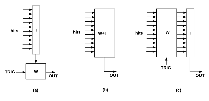
Figure 29 compares schematically three readout architectures, where the buffered storage of hit data is represented by W for wait, and the motion of hit data by T for transfer. In the classic column drain architecture of 1st generation chips (fig. 29 (a) ), all pixels in a column share a data bus that only one pixel at a time can use. As soon as a pixel is hit, it tries to grab the bus and transmit its data. The bus is arbitrated so each hit pixel must wait its turn. This column bus is itself a single server queue, just like the case of full chip readout. The bandwidth of the bus must exceed the incoming hit rate for this to be viable. Equation (15) shows the probability for waiting a time greater than in such a simple single server queue 101010In Kendall notation [126] this is an M/M/1 queue,
| (15) |
where is the input hit rate and is the output bandwidth. For a pixel hit rate , , where is the number of pixels served by the bus. Hits must be transferred within a short time, , as there is no place to store them within the pixel array. Therefore, to avoid hit loss, , which means that . Since is small, one must have : the well known condition that column drain needs a high bandwidth. Implementation of a trigger buffer in 1st generation chips was at the chip bottom, requiring all hits to be transferred out of the pixel matrix. Only after storage in the periphery was the trigger selection applied.
The LHC-b Velopix readout chip implements a read-all architecture using a shift register (SR) for transferring hit data instead of a bus. This is represented by fig. 29 (b). The SR not only transfers data, but is also temporary storage. The output bandwidth of the SR is simply the clocking speed (assuming one pixel hit is read out per clock cycle). But unlike an arbitrated bus, each pixel sees a different output bandwidth. The very first pixel feeding the SR sees the full bandwidth, but the next pixel sees less bandwidth because occasionally it will be blocked by data from the previous pixel already in the SR. Thus, pixel sees an output bandwidth , where is the hit rate of the pixel. Because the SR stores hits, the short transfer time requirement of column drain is removed, and one just needs (as opposed to ). If all pixels have the same hit rate , one needs , where , as before. Since the last pixel sees the smallest output bandwidth, its waiting time is the longest, so one can choose such that the last pixel waiting time is less than the time between hits. This architecture is particularly well suited to the highest rate chips in the Velopix detector, because the hit rate is not the same in all pixels. The pixel nearest the beam line has the highest rate, and also happens to be the pixel farthest from the readout– that is, the first pixel in the SR. The last pixel in the SR has the lowest hit rate. Thus, the pixel dependent hit rate nicely follows the pixel dependent output bandwidth .
Starting with the 2nd generation triggered ROICs, high logic density permitted the implementation of local hit storage within the pixel matrix (fig. 29 (c) ). The input rate to the column bus is reduced as , where is the trigger rate and is the bunch crossing period. If the readout time can be long, then one can have , which makes for a very relaxed column bus transfer bandwidth requirement. In addition to higher hit rates, this relaxed requirement has been exploited to make larger ROICs (more pixels per column bus). Instead of being limited by the transfer rate, the hit rate that can be handled is limited by the amount of memory that can fit in the pixel matrix. All hits must be stored for the entire trigger latency, so the memory needed scales like . The longer the trigger latency the smaller the hit rate that can be handled.
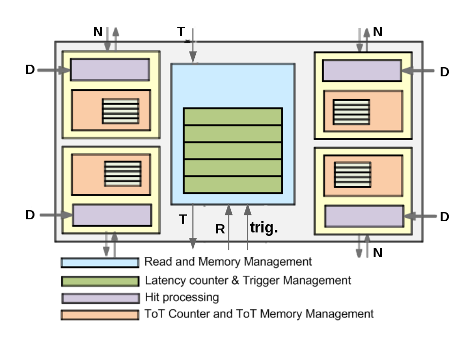
The local storage of hit data does not make efficient use of memory when done at the individual pixel level. This is because the mean time between single pixel hits is longer (but not much longer than the trigger latency). For example for 50 kHz single pixel hit rate and 5 s trigger latency, the average number of hits per latency period is 0.25. Using Poisson statistics, one would need to store up to 3 hits per pixel in order to keep 99.9% of hits. We refer to this number (3 in this example) as the buffer depth. Instead, grouping pixels into regions with shared storage significantly reduces memory needs. Consider grouping 4 pixels together. If the 4-pixel region average hit rate were 1 hit per latency period, then, using Poisson statistics, one would need a buffer depth of 5 region-hits per latency period in order to keep 99.9% of hits. That is only 5/4 = 1.25 buffer locations per pixel instead of 3 as before. But the advantage is even greater, because in a pixel detector the hits among neighbor pixels are correlated (charged particles produce clusters). The correlation between pixels means that the region hit rate is less than the single pixel hit rate times the number of pixels per region. The amount of correlation depends on sensor and detector geometry. Charge information, on the other hand, must be stored for every hit pixel regardless of how the pixels are grouped, and this reduces the advantage of having many pixels per region. The simplest approach is to store a fixed number of charge bits per pixel times the buffer depth. Suppose in the above example one stores 10 bits of region hit arrival time and some flags, plus 4 bits per pixel charge information. If storage is independent per pixel, each pixel must store 14 bits per hit times buffer depth of 3, or 42 bits per pixel. Conversely, in a 4 pixel region, one must store bits per region hit times buffer depth of 5, or 32.5 bits per pixel. The FE-I4 ROIC architecture is based on a 4-pixel region along these lines [18], shown schematically in fig. 30.
To take full advantage of larger regions (or to efficiently store higher precision charge information) one needs a more sophisticated storage mechanism that allocates memory only to hit pixels, and does not store zeros for pixels below threshold in the same region. Effectively, hit information must be transferred as soon as it is produced from the pixels to a central storage. This should evoke the column drain architecture of fig. 29 (a). A large region with arbitrated storage can be labeled as 'region drain' and can be analyzed the same way as column drain. The main problem of column drain was the high bandwidth requirement for the column bus, . But given a bus bandwidth , one can always make small enough by reducing the number of pixels on the bus, , since ( being the single pixel hit rate). In other words, column drain can accommodate high hit rate for a small enough ROIC. Therefore, a large, high hit rate ROIC could be built as a matrix of 'little chips' each with column drain architecture. It is interesting that the architecture evolution moved away from column drain because it could not scale to larger size (or to higher hit rate for fixed size), in favor of region architecture, for which size and hit rate are decoupled. But, evolving to large regions eventually leads to the same point as replicating a column drain architecture many times, as a way to achieve both large total size and high rate.
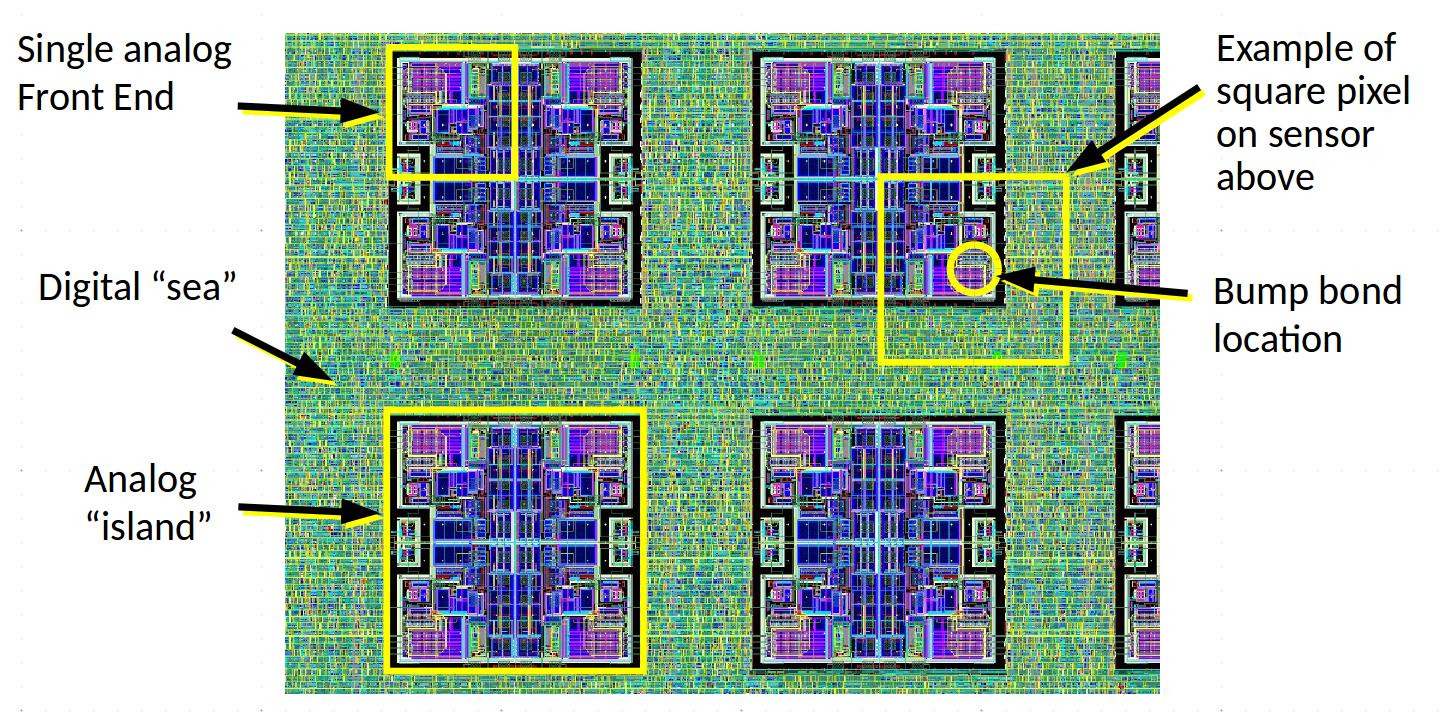
Third generation ROICs will continue to expand region architectures. While the basic 4 pixel region described above probably represents a sweet spot for efficient memory usage, the use of larger regions is being explored [127]. Already in the 2nd generation an important change took place, in which a ROIC core went from being a collection of pixel circuits, stepped and repeated, to a collection of regions, stepped and repeated. A 3rd generation ROIC will be a collection of digital cores, stepped and repeated. A core is not the same as a region and can in fact contain many regions. A core is simply the smallest stepped and repeated instance of digital circuitry. A relatively large core allows one to take full advantage of digital synthesis tools to implement complex functionality in the pixel matrix, sharing resources among many pixels as needed. Large cores can have 2 dimensional digital connectivity, removing the constraint on all previous ROICs that communication could only take place up and down pixel columns, but not along rows. Figure 31 shows a layout detail from the RD53 Collaboration in which identical 4-pixel analog front end islands can be seen completely surrounded by synthesized logic. The core logic has been dubbed 'digital sea' to stress that it results in a different and variable environment surrounding each analog island (depending on where synthesis tools place gates and connections). This is a radical departure from the single pixel step and repeat, perfectly symmetric environment of the 1st generation, raising potential concerns about systematic variations within the pixel matrix. The FE65-P2 prototype [123], which implemented 4 by 64 pixel cores, has shown that with modern isolation techniques (see section 4.6) excellent uniformity can be achieved within a large synthesized core.
4.8 Input hit rates and output data transmission (electrical)
Hit rates and output bandwidth increase by an order of magnitude or more between between 2nd and 3rd generation ROICs. For both past and planned detectors, output data are transmitted electrically for at least the first meter away from the ROIC (optical links are covered in section 4.9). The LHC-b experiment is implementing a full triggerless readout system in the upgraded VELO detector using the Velopix IC [12]. They are able to do this because the hit rate, while very high, is not extreme, and the experiment has a fixed target geometry, allowing data cables to be placed outside of the physics acceptance. The ATLAS and CMS experiments, on the other hand, must contend with an order of magnitude higher hit rate per ROIC and have nearly 4 physics acceptance, so most data cables must pass through the active volume. They will therefore use triggered readout. However, the trigger rates will be an order of magnitude higher than today, which combined with busier events will make for a 20- to 40-fold readout bandwidth increase for 3rd generation ROICs. The LHC-b hit rate is projected to be 1.6 GHz/cm2 for the most occupied pixel, but as the rate decreases almost quadratically with radius and the modules are perpendicular to the beam, the average hit rate in the most occupied ROIC is 0.3 GHz/cm2. In contrast, for the ATLAS and CMS upgrades all pixels (and therefore all ROICs) in the innermost barrel layer have similar hit rates, projected to be near 3 GHz/cm2 for a 3.2 cm layer radius.
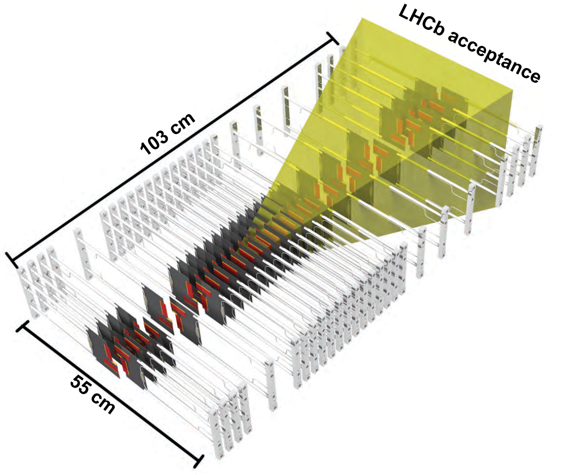
Figure 32 shows the geometry of the LHC-b VELO upgrade. The fixed target geometry allows for high bandwidth data transmission with almost no cable mass in the active volume. The Velopix IC supports 4 parallel differential outputs at 5.12 Gbps each, fed by the shift readout architecture described in section 4.7. The data use a fixed frame custom format, where each frame contains a time stamp and a bit map for a group of 8 pixels (no charge information is recorded, just hit/no hit). Reading individual pixels instead would use 30% more bandwidth, because it would not take advantage of the clustered nature of pixel detector hits.
A theoretical discussion of lossless data compression in pixel detector readout can be found in [128], which explains that the information content (entropy) is roughly proportional to the number of clusters and the achievable compression depends on cluster size. The 30% compression afforded by multi-pixel frames in Velopix is not the maximum possible compression, but is adequate for LHC-b needs. The projected data packet rate for the most occupied chip is 520 MHz, while the Velopix output consisting of 4 links at 5.12 Gbps each will saturate at a 640 MHz packet rate.
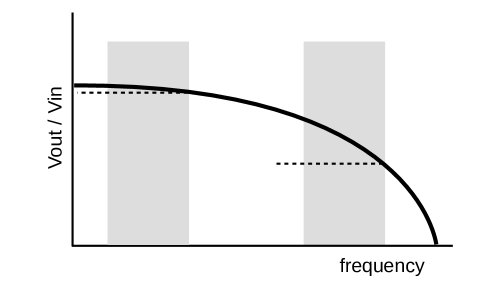
The ATLAS and CMS upgrades plan an output bandwidth of 5.12 Gbps per ROIC, which is actually less than 25% of the LHC-b maximum because the planned ROIC size is slightly larger. A critical difference is that ATLAS and CMS must have longer cable runs and at the same time minimize data cable mass, which means tolerating a high transmission line loss (meaning signal attenuation, not data loss). Figure 33 shows conceptually the attenuation of a signal passing through a lossy transmission line. Two vertical gray bands represent low and high bit rate transmission. These bands have a lower cutoff, rather than extending to zero frequency, because DC-balance has been assumed. DC balance avoids low frequencies by guaranteeing at least one transition every bits (e.g. for the 8b/10b encoding ). If the attenuation curve within a gray band is flat, that means the signal shape will not be distorted: a good condition for error-free transmission. This makes it obvious why DC balance improves transmission: the narrower the band, the smaller the variation of the attenuation within the band. However, for the band at high bit rate, even with DC balance there is a large variation of the attenuation within the band. This situation can be improved with equalization, indicated by the horizontal dashed lines. Equalization attenuates lower frequencies more than higher frequencies (the opposite of what cables do) to achieve a flat response within the band. All this is well known textbook material [129], but is only now playing a critical role in pixel detector design. The telecommunications industry and consumer electronics have long ago optimized performance in lossy transmission situations. As a consequence, particle physics designs are moving towards more sophisticated commercial protocols and solutions. State of the art equalization included in commercial FPGA’s can achieve reliable transmission with line losses as high as 28 dB. While prior ROICs (for example FE-I4) have used 8b/10b encoding, the RD53A ROIC will use an open source commercial protocol implementation of 64b/66b encoding, including a multilane version for balancing data over four 1.28 Gbps outputs. Equalization will be an integral part of future systems: RD53A drivers will have pre-emphasis capabilities, which boost high frequencies at the transmitter (sending a purposely distorted signal to counteract the cable distortion) and receivers with different types of equalization are also being developed [130, 131]. Receiver equalization has the advantage that it can be more easily made adaptive, so that it does not have to be manually tuned for every link or every time environmental conditions change. Even with these techniques, because of various constraints including radiation damage, the ATLAS experiment aims to keep line losses at 20 dB or less.
It is clear from fig. 33 that there is a limit beyond which the signal is completely lost and no amount of equalization can recover it (recall the 28 dB mentioned above). The only remaining option to further increase the data rate on such a cable is to use multiple logic levels at a given frequency. For example with 4 logic levels instead of two, one can send two bits per clock cycle instead of one. The problem is that the available output voltage must then be divided among the logic levels. The voltage difference between two levels is , where is the number of levels. Noise can cause confusion between levels, so one can use multiple levels as long as . This also applies to standard equalized signals with two logic levels (=2), which means that one cannot go too far to the right in fig. 33. But one can go further to the right for than for , so whether multi-level transmission is advantageous or not depends on how fast the cable transmission cuts off. What should be clear from this discussion is that using higher voltage at the driver (for a given noise level) will increase the achievable data bandwidth. Commercial IC interface logic operates at a higher voltage than the core transistors, thanks to thicker gate oxide. But such thick oxide devices are much less radiation tolerant and therefore not adequate for pixel detector applications. For 65 nm the maximum operating voltage of core transistors is 1.2 V. Future development could include multi-level transmission using stacked core transistors, where the voltage difference between all levels remains around 1 V instead of 1.2 V/. A final problem facing high speed drivers in pixel ROICs is that high speed logic is more vulnerable to radiation damage than low speed logic, because switching speed depends on transistor gain. This could be a pixel-specific reason favoring the use of multiple logic levels at lower clock speed over the standard two levels at higher clock speed.
While not strictly an ROIC issue, the quality of available cables is a critical point for data transmission. Commercial data cables are not developed with low mass requirements and contain dielectric materials that are not radiation hard. Therefore, development of custom cables for low mass, radiation hard, high speed transmission is an ongoing activity. This includes flexible printed circuits [132], short run unshielded twisted pairs, long run shielded twisted pairs, and twin-axial [133].
4.9 Optical and wireless transmission
The technical design report for the original ATLAS pixel detector [134] specified optical links located on the module, less than 1 cm away from the closest ROIC, with optical fibers forming part of the module interconnect. Such an arrangement was never realized and designs have instead moved further away from this model. There are three reasons why optical conversion is located some distance away from pixel modules: radiation, geometry, and reliability. Fibers and active optical elements both suffer radiation damage [135, 136] and are not currently suitable for environments exceeding 100 Mrad. For the laser drivers, but not the fibers, there have been promising developments in silicon photonic systems using Mach-Zehnder interferometers rather than switching lasers, following the trend in commercial high speed optical links [137]. But customization of such devices for particle physics has so far not been widely successful. Geometrically, pixel detectors are compact, with highly constrained cable routing to achieve hermetic coverage. Routing of fibers to all modules in a pixel detector would require complex manipulation of unjacketed fibers, which are fragile and have a minimum bend radius that must not be exceeded. Electrical cables are much more forgiving and can tolerate any bend radius.
4.10 Power distribution
The 1st generation ATLAS and CMS pixel detectors achieved a power distribution efficiency of approximately 25%. This means that 75% of the power delivered by rack power supplies was dissipated in cable IR loss and voltage regulators. Since the only current return path is thorough the detector, the power delivery efficiency is given by , where (load voltage) is the voltage across the detector elements connected to each single power supply channel, and is output voltage at the power supply. Inefficient power delivery was recognized as a problem, but nevertheless the 1st generation detectors could be built using simple, direct power delivery to each module within a material budget considered acceptable. The planned high luminosity upgrades, on the other hand, face a much greater power delivery challenge. Not only will the detectors be larger, but the deep submicron electronics used will operate at half the voltage yet with slightly more power per unit area. This leads to a total detector current requirement an order of magnitude higher than present detectors.
However, the current that can be delivered from rack power supplies to the ATLAS or CMS inner detectors is limited by external factors. The resistance of the cable plant supplying the inner detector has a lower practical limit, , imposed by mass and space considerations. At the same time, the IR-loss heat load on the subdetectors traversed by these cables is limited to so as not to degrade their performance. Therefore, the rack power supplies are only allowed to deliver at most . Approximate values for ATLAS are kW and m (round trip), yielding kA. The only free parameter left to control the power supplied to the detector is the load voltage . For an expected 3rd generation ROIC power of order 0.6 W/cm2, a 10 m2 pixel detector would need a load voltage of 12 V to deliver the 60 kW total power using 5 kA of rack supply current. Since the ROIC operating voltage =1.2 V, directly powering the ROICs is out of the question: power conversion at the load is required.
From the above discussion, the voltage conversion ratio required for HL-LHC pixel detectors is of order 10. Two conversion methods have been extensively investigated: DC to DC converters and serial power. The DC-DC conversion technologies investigated include magnetic switching using air core inductors [138, 139] 111111Ferromagnetic cores cannot be used in the strong tracker solenoid fields., piezo-electric converters [140], and capacitor charge pumps [141]. While discrete DC-DC converters have now been developed to be compatible with LHC experiments [139], their use on pixel detector modules would result in too much added mass due to the high current per unit area required. Fully on-chip DC-DC conversion has been investigated [142] as this would not add any mass, but has not yet matured enough for consideration in the construction of HL-LHC detectors.
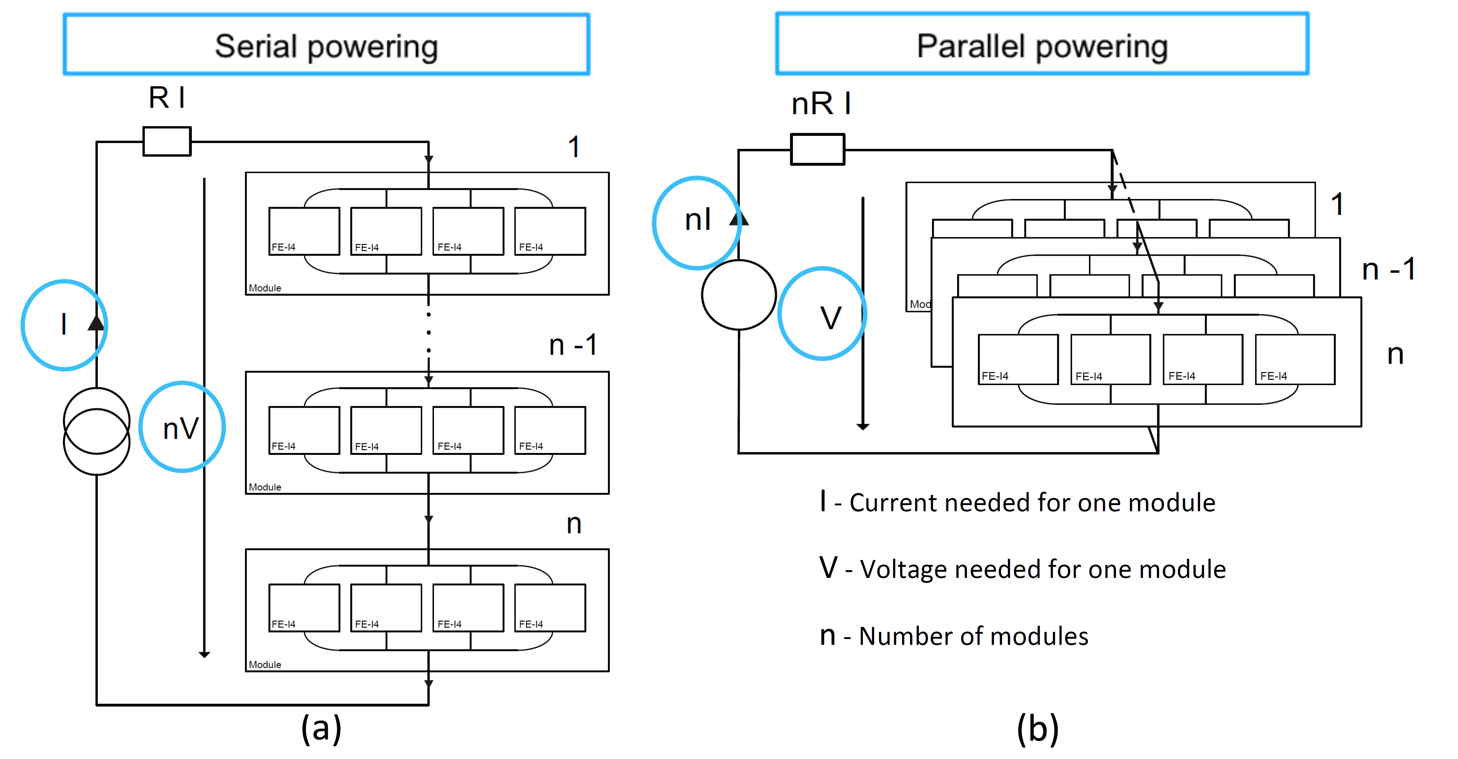
Serial power achieves power conversion without added mass by connecting devices in series and operating with constant current instead of constant voltage power supplies. Figure 34 compares 4-chip modules in serial vs. parallel power configurations. The serial configuration only needs two conductors and one power supply channel to serve modules. Because , the power delivery efficiency () can be increased as needed by increasing . Furthermore, constant current supplies are better suited to delivering power over resistive cables than the more common constant voltage supplies. Constant current powering is used commercially with very long, resistive cables, for example in undersea communications lines [143]. However, the requirements of pixel detector operation are very different and a custom serial power technology solution had to be developed. Serial power has been found to be reliable to implement and compatible with pixel [144, 145, 146] (and strip [147]) detector operation, and is the baseline for both ATLAS and CMS HL-LHC pixel detector designs. Implementation requires specialized constant current regulators, which have been developed [148] and included in the FE-I4 ROIC and the RD53A ROIC design. Prior efforts used simpler shunt voltage regulators [95].
4.11 Future development
Even as monolithic solutions mature, hybrid technology with special purpose ROICs will continue to be necessary for the highest rate capability and the implementation of new functionality, such as fast timing. Looking to industry we find that the monolithic CMOS sensors in modern smartphones are actually 3D integrated devices. To the extent that such technology becomes open to low volume third party customization, monolithic devices for particle physics could also consist of multiple layers with processing and readout in small feature size CMOS exactly as conventional hybrid ROICs. In the coming years ROIC R&D will explore smaller feature sizes, with 28 nm being the likely candidate to follow 65 nm for 4th generation ROICs within a ten year horizon [149].
The 4th generation ROICs will add even more sophisticated digital functionality with minimal, but high speed analog front ends to enable fast timing. The operation of the individual pixels will likely be continually monitored and adjusted in real time with no need for storage of configuration data or lengthy calibrations. Improvements in communication and data compression will continue. Single lane output switching frequency will likely not increase beyond 5 Gbps due to issues with radiation tolerance of high speed logic, but data rate could be increased by making use of multi-level logic, essentially following industrial trends to maximize data rates in existing infrastructure originally designed for lower bandwidth. The point in particle physics is not to fit into existing infrastructure but to use the lowest possible mass cables. It is also possible that improvements in data cables themselves will be realized (higher bandwidth for lower mass), for example by replacing copper conductors and/or aluminum shields with carbon nanotube 'rope' or graphene foil, respectively. Some use of wireless technology is possible, if nothing else to facilitate testing by being able to communicate during detector construction/integration without physical connections. Finally, on-chip power management will surely increase, dynamically managing core voltage levels and possibly adding on-chip DC-DC conversion with high ratio (4 or more) providing an alternative to serial power.
5 Advanced materials: new possibilities for supports and cooling
The original ATLAS and CMS pixel detectors achieved an amount of material around 3.5% of a radiation length per layer at normal incidence [150, 151]. Of this, 0.5% was due to silicon (sum of ROIC and sensor). Since then, significant advances in mechanical support (section 5.2) and cooling (section 5.1) have taken place, and future ATLAS and CMS detectors are projected to be more than 50% lighter, between 1% and 1.5% per layer, out of which 0.3% will be silicon. Still lower mass is achieved with monolithic instead of hybrid technology, of order 0.3% per layer [152, 153]. The reason is not only less silicon, which can at most save 0.3%, but less stringent cooling requirements for monolithic sensors with small pixels and small depleted volume (and therefore small leakage current and no thermal runaway issues). However, monolithic active sensors compatible with high rate and radiation are still under development (see chapter 6).
Some critical developments have been CO2 evaporative cooling, new composite materials, new methods for structure design and fabrication, and serial power distribution. Serial power distribution, which is an electronic system development, has been covered in section 4.10.
5.1 Cooling
The high power density and large extent of pixel detectors at the LHC demands a coolant that can transport a large amount of heat with low mass flow. Since evaporation can remove more heat for the same mass flow as single phase liquid cooling, it is preferred. Gas phase (air) cooling has been used for the STAR Heavy Flavor Tracker [154], but that detector is compact (20 cm active length and 0.2 m2 active area) and based on CMOS sensors that do not need to be kept cold. Nevertheless, 0.2 W/cm2 was removed with 10 m/s simple air flow (no fins or heat transfer enhancement features). An important advantage of evaporation is the absence of a temperature gradient along cooled structures. With an evaporative cooling system, the coolant temperature is fixed, regardless of heat load (for load less than maximum capacity). The heat is absorbed by the liquid to gas phase transition, so the difference between inlet and outlet of a cooled structure is the liquid fraction (high at the inlet and lower at the outlet). The maximum load capacity is reached when all the liquid has evaporated - a condition called dry-out, which should never be reached in a properly working system.
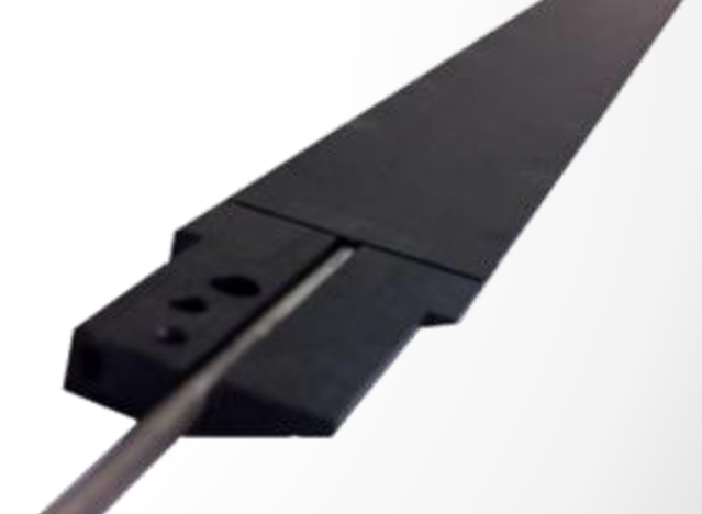

CO2 is an ideal evaporative coolant for tracking detectors because it offers heat transfer coefficients an order of magnitude higher than traditional refrigerants, and its high evaporation pressure (around 50 bar) means small produced vapor volume, resulting in small diameter tubing. However, pressure safety is one of the challenges of using CO2, requiring a rating of 200 bar throughout. The use of evaporative CO2 for tracker cooling was pioneered by the AMS experiment [155], and in colliders by the LHC-b experiment. It was later adopted for the ATLAS IBL upgrade (fig. 35) and the CMS pixel upgrade. For a review see [156]. The original ATLAS and CMS detectors used other coolants that were better established at the time and did not need very high pressure plumbing. ATLAS used evaporative C3F8 [157], while the original CMS pixel detector used monophase cooling with C6F14.
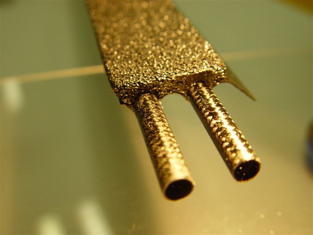
While aluminum has been used for cooling pipes in more conventional (fluorocarbon) evaporative systems [157], it is very difficult to prevent corrosion in aluminum pipes during detector construction [158], and weakening of pipe walls due to corrosion can be fatal for a high pressure system. Therefore, for many present CO2 cooling systems the pipe material of choice is titanium, which is corrosion resistant and high strength (so can withstand high pressure with thin walls), yet relatively low mass. The main reduction in mass from CO2 cooling comes not from the pipe material, but from the very small diameter pipes that can be used. Other materials have also been explored, most notably carbon fiber, for which braided fiber tubes are a common industrial product and so it is possible to produce braided pipes, but so far this has not been adopted. Figure 36 shows a prototype support with 2 mm diameter braided pipes embedded in carbon foam. For a review of pixel detector cooling and thermal management materials see [3].
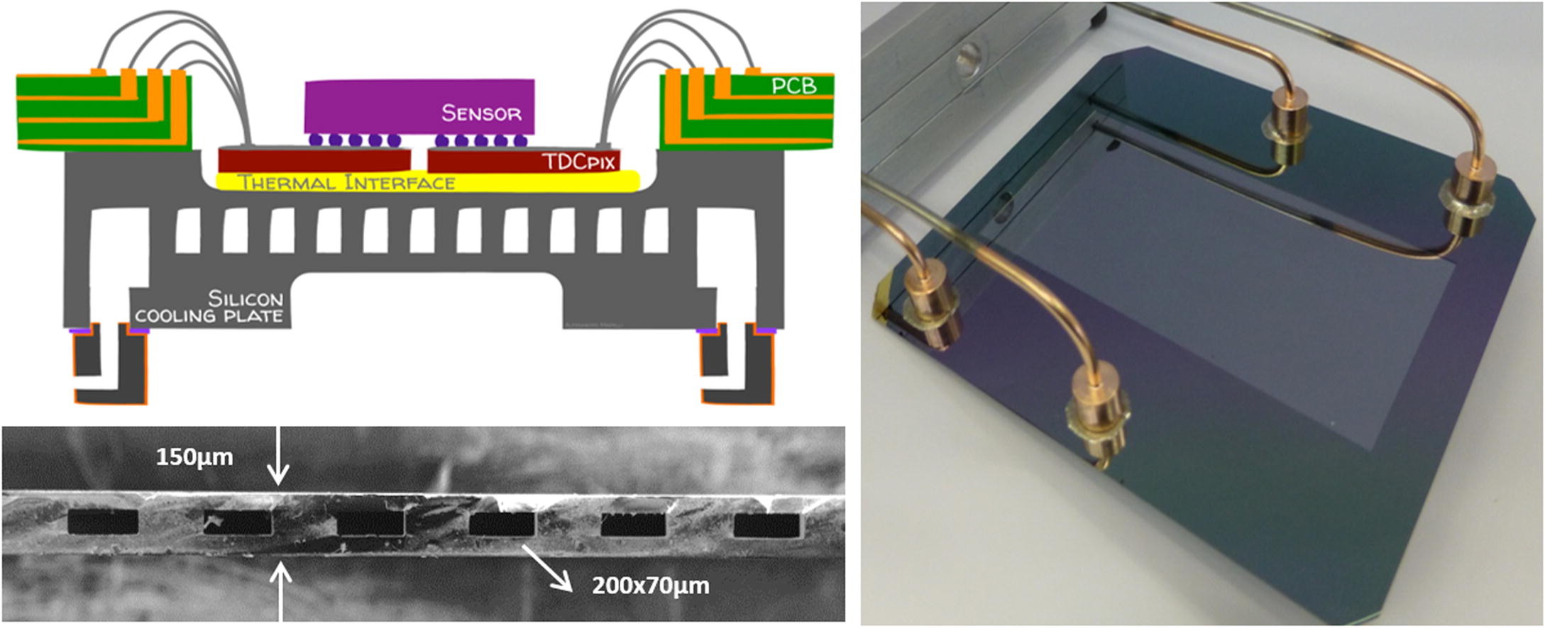
A more recent development has been the use of silicon micro-channels with CO2 cooling, in order to achieve very high cooling capacity with even lower mass than possible with separate mechanical supports cooled with metal pipes. This is suitable for fixed target geometries where mass can be placed immediately outside active elements, and has been pursued in the NA62 Gigatracker [159] (fig. 37) and LHC-b [160] upgrades.

For hybrid pixels, detector lifetime and cooling performance are closely coupled. The irradiated sensor leakage current scales with temperature (rule of thumb is that current doubles every 7∘C), while the temperature depends on the power dissipated in the sensor, which in turn depends on leakage current. This leads to the well known condition of thermal runaway above a certain temperature [161]. The behavior can be captured by a simple model with the cooling performance of mechanical supports represented by a specific thermal resistance (cmC/W), also referred to as Thermal Figure of Merit (TFM) [162], as shown in fig. 38. With an evaporative cooling system, the coolant temperature is fixed, so the sensor temperature rises linearly with power dissipation, and the proportionality constant is the TFM. Thus the TFM defines positive feedback that leads to thermal runaway. High TFM means large positive feedback and therefore early thermal runaway (short lifetime), while zero TFM would be ideal. The mechanical supports of 1st generation ATLAS and CMS pixel detectors as built achieved a TFM of 30∘C cm2/W, while support structures prototyped for the HL-LHC upgrade detectors have achieved a TFM as low as 10∘C cm2/W (can expect 15∘C cm2/W for as built detectors). This impressive advance has been obtained by utilization of new, more performant carbon composite materials, such as thermally conductive carbon foam [163]. High thermal conductivity, low mass foam allows one to take advantage of the CO2 cooling by providing a way to efficiently collect heat from a large area module and couple it to a small diameter tube. Commonly used values of foam density and thermal conductivity are 0.2 g/cm2 and 40 W/m/K, respectively121212Foam thermal conductivity scales approximately with density, which can be adjusted in production..
5.2 Supports
Support structures must combine the excellent cooling capacity discussed in section 5.1 with low mass and mechanical stability high enough to maintain module positions to within 10 m. Carbon composite designs and methods have enabled substantial mass reduction. A successful design approach for inner pixel layers has been the use of coupled layer structures. Single layer supports spanning long distances (tens of cm) suffer gravitational and vibrational deformations that elements are too large without auxiliary stiffening, such as shells or frames, and the mass of these elements also contributes to the detector radiation length. By coupling layers in pairs, structures can be made stiff enough over long spans without auxiliary support structures, thanks to the large moment of inertia or the coupled layers. The ALICE and STAR experiments used box beam structures for this purpose [164, 153]. In the case of STAR the approximately 30 cm long structures were held cantilevered from one end only. A further development in this direction, providing similar mass and stiffness with additional usable space, higher nesting freedom, and monolithic construction uses an I-beam rather than a box beam shape [165] (fig. 39 (a) ). Other large moment of inertia structures use truss-like assemblies [152].
New materials such as foam have also enabled development of supports with more complex geometry that position modules with some tilt angle relative to the colliding beam direction [166]. An example of a support called Alpine [167] using foam pedestals is shown in fig. 39 (b). Endcap pixel detectors have seen similar evolution, with CO2 cooling and carbon composite developments allowing for lower mass and greater design freedom [8]. Planned high luminosity upgrades of ATLAS and CMS will have greater acceptance coverage and therefore larger endcap systems [166, 168].
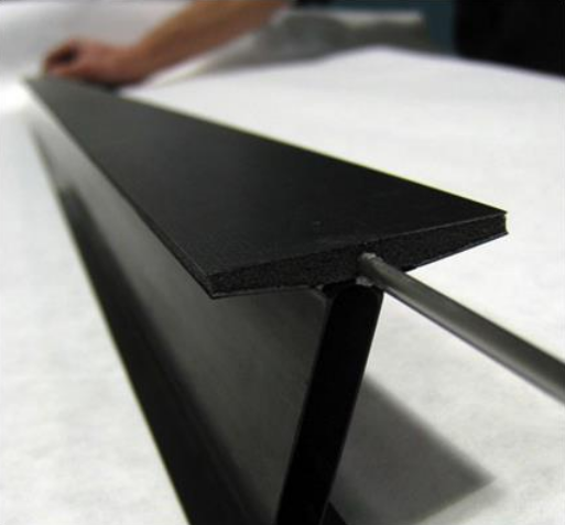
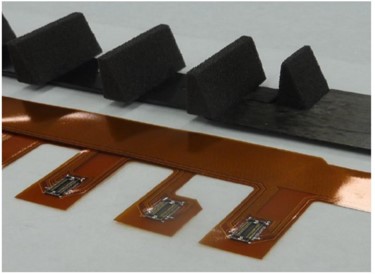
6 CMOS active sensors: towards monolithic pixels
The many advantages of hybrid pixel detector technology have been highlighted throughout this report. However, the hybrid choice also has some notable disadvantages. Hybrid pixels constitute a relatively large material budget, typically more than 1.5% X0 per detector layer (ATLAS IBL), distributed among the module components and the cooling and support structures. The module production including bump-bonding and flip-chipping is complex and laborious, leading to a large number of production steps. Consequently, hybrid pixel detectors are comparatively expensive.
Modern CMOS imaging sensors instead make use of 3D integration to combine high resistivity and fully depleted charge collection layers with high density CMOS circuitry, in order to achieve high speed and high collection efficiency (for low light operation). Such a combination of fully depleted high resistivity silicon with CMOS readout sounds like a requirement from particle physics, not from consumer electronics, but smartphone image sensors have independently evolved in this direction for different reasons and with different optimization. For example, the pixels are very small ( 20 m2) and the depleted layer is very thin (few m). Nevertheless, their out-of-the-box use for radiation and particle detection is being explored [170]. Such high end fabrication processes are currently not available to be customized for particle physics.
The following sections address current developments towards fully depletable, radiation tolerant, and high rate capable monolithic pixel devices, inheriting in part from successful adaptation of CMOS camera type sensors with thick epitaxial layers. The development of fully depletable devices becomes feasible by exploiting advances in the CMOS industry, in particular the availability of multi-well technologies for both low and high resistivity substrate wafers.
6.1 From MAPS to DMAPS
Employing commercial CMOS technologies to produce a monolithic (rather than hybrid) pixel detector in which pixel sensor and electronics circuitry form one entity, has first been proposed [171] and realized [172] in the early 1990s. Some years later, Monolithic Active Pixel Sensor (MAPS) detectors were introduced [173, 174], exploiting as the sensing volume an epitaxial layer often grown on top of the lower quality substrate wafer and hosting the CMOS circuitry. The thickness of this epi-layer typically is in the range of m, where thicker layers are often used in processes addressing CMOS camera applications (fig. 40(a)).
For particle detection the charge deposited in the epi-layer can be as large as 4000 e- for a typical thickness of 15 m. Since the epi-material usually has low resistivity and the allowed biasing voltages are low in CMOS technologies, the epi-layer usually is depleted only very locally around the charge collection node. The deposited charge of a traversing particle therefore is mostly collected by diffusion rather than by drift. This renders the signal generation slow and incomplete (not all charges arrive at the collection node) and is, besides the lower radiation hardness, the main reason why this original MAPS technology is not suited for high rate applications as needed in LHC pp-experiments. Furthermore, other n-wells, e.g. those hosting PMOS transistors, act as competing nodes for charge collection. The latter can and must be cured by additional deep p-well protections as is also shown in fig. 40(a).
MAPS pixel detectors have been successfully used in lower than LHC rate and low radiation experiments, such as the STAR experiment at RHIC [175, 176]. Also the ALICE ITS Upgrade [152] has chosen MAPS pixels based on the 180 nm CMOS node offered by TowerJazz with 6 metal layers [177]. Note, however, that the expected radiation level for HL-LHC ion collisions is 700 krad and neq/cm2, respectively, i.e. 1500 times lower than for LHC pp-experiments.
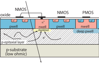
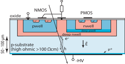
Depleted (D)MAPS
In order to further develop CMOS pixel detectors for LHC type rate and radiation applications, improved development lines have been pursued leading to depleted monolithic active pixel sensors (DMAPS) [26][178]. The goal of this new development is to employ commercial CMOS technology with some modifications to obtain sufficient signal and fast timing in monolithic CMOS designs, while maintaining charge collection via charges drifting in an electric field inside the chip’s substrate. The technology and the sensing properties must survive the radiation environment at the HL-LHC, at least in the outer layers, far enough from the interaction point, such that the radiation levels are similar to those presently encountered at the inner layers, i.e. 100 Mrad ionisation dose and cm2 particle fluence, respectively.
The development of such detectors much relies on recent advancements and freedom in CMOS technologies, offered in particular by vendors interested in market corners away from mass IC production and offering process add-ons or modifications. The goal is to achieve some (50–100m) depletion depth
| (16) |
where is the substrate resistivity and V is the bias voltage, yielding a reasonably large signal ( 4000 e-) with fast and in-time efficient charge collection, while avoiding long collection paths on which charges can be trapped after irradiation. At the same time full CMOS functionality shall be maintained, i.e. equal and unconstrained usage of PMOS and NMOS transistors and no or little interference of electronics signals and detector signal pulses.
DMAPS detectors in particular exploit the following CMOS technology features:
-
1.
High voltage technology add-ons (from automotive and power management applications) that increase the voltage handling capability and create a depletion layer in a well’s pn-junction of depth in the order of 10–15 m.
-
2.
Medium to high (100cm) resistivity 8′′ silicon substrate wafers, accepted and qualified by the foundry. A depletion layer develops due to the high resistivity with only moderate bias voltages applied from the electronics side or a (specially processed) backside contact.
-
3.
Multiple nested wells (see also chapter 4) that can be used to isolate transistors and shield deep well potentials in order to optimize charge collection. The foundry must accept some process or design rule changes in order to optimise the design for HEP applications.
-
4.
Backside processing add-ons allowing for example a backside biasing contact acting as an additional field shaping potential of the device.
Interest in CMOS pixels for HL-LHC has been aroused by its potential for low cost and the feasibility of large area monolithic devices in outer tracker layers when stitching is employed, but also out of intellectual curiosity about whether a one-piece pixel detector can be developed for HL-LHC environments demands.
DMAPS capacitances

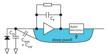
Figure 41 shows the main capacitances in a DMAPS design that contribute to the total amplifier input capacitance of a pixel cell. In addition to the pixel-to-pixel (Cpp) and pixel-to-backside (Cb) capacitances, also present in any other sensor design, inter-well capacitances to the well sides (CSW) and between deep n-well and p-well (CWW) play a significant role. In particular, if the deep n-well is large (large fill-factor, see below) CWW can achieve significant values (as large as 100 fF for 10 000 m2 pixel area) increasing the total capacitance. This is to be compared to typical hybrid pixel capacitances of 120 fF (planar) and 180 fF (3D-Si) [179]. A large amplifier input capacitance directly enters the thermal noise (and also 1/f noise) figures of a pixel detector with CSA readout and shaping as well as the detector response time :
| (17) |
where is the feedback capacitance, the transconductance, the shaping time, and is the Boltzmann constant times temperature.
While it may be possible to cope with additional input capacitance as a noise factor, e.g. by increasing (which increases power), the inter-well capacitance also couples the CMOS electronics with the sensor volume as illustrated in fig. 41(b). This requires careful circuit design and special measures to prevent digital activity from coupling to the sensor part, thus faking particle signals. An alternative is to place the digital logic away from the active sensor part (n-well), at the price of a smaller fill-factor (see below).
Fill-factor choices
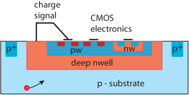
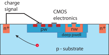
Figure 42 shows two principal variants of a pixel cell arrangement. While in fig. 42(a) the entire CMOS electronics is enclosed in the deep, charge collecting n-well, in fig. 42(b) the deposited charge is collected at a small n-well located outside the electronics area. A large fill-factor provides good charge collection properties over the entire pixel area with on average shorter travel distances and hence smaller trapping probabilities after irradiation, but it suffers from a comparatively large inter-well capacitance contribution ( 100 fF) as discussed above leading to larger noise figures and slower timing. Increased power (compared to hybrid pixels) for the same pixel area is needed to cope with the larger capacitance. Most developments so far have chosen this variant to minimize radiation hardness issues, the main challenge at the HL-LHC. Note that with the advancement of CO2 cooling a change in the power bill does not linearly translate into material. Thermal conductivity of the components is the key parameter (see also section 5.1). For example, for a cooling tube embedded in a carbon foam, increasing (decreasing) the power by a factor of 2 leads to a material increase (decrease) of 10 or 20% [180].
The small fill-factor variant on the other hand promises node capacitances of only 5–20 fF and hence excellent noise and timing performance. However, the radiation tolerance is an issue, given that on average the drift distances of signal charges are longer for same cell size. Small pixel sizes are therefore beneficial for a small fill-factor design at the expense of power density.
Substrate resistivity
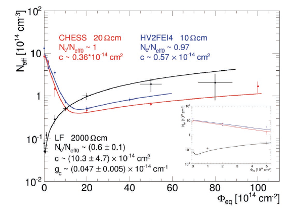
According to eq. (16) high resistivity is a means to obtain adequate signal sizes by sufficient depletion depth at moderate bias. Figure 43 [181], however, shows that independent of the starting substrate resistivity, over a large range of resistivities (10 cm–2 kcm) one observes that after a fluence of about 1015 neqcm-2 the effective space charge concentrations approximate each other at a level of about cm-3 corresponding to about 100 cm. This effect is commonly attributed to radiation induced acceptor removal, setting in earlier at higher p-doping concentrations and eventually leading to similar concentrations. Therefore, for high radiation applications, the starting resistivity is not very critical, and in fact an intermediate (100 cm - 1 kcm), not too high initial resistivity may be advantageous as this will lead to a fairly constant charge collection throughout the lifetime.
6.2 Designs and technology variants
The high energy physics community has targeted different prototyping designs with various foundries providing standard CMOS technology add-ons necessary to cope with the given demands. The emphasis at the start was either on dedicated high voltage technologies [26] or on technologies accepting high resistivity substrate wafers for processing [182]. It turned out that both, mid to high resistivity ( kcm) as well as sufficient bias ( 150 V), are needed for good performance under irradiation. The general approach of different groups has been in three prototyping steps.
-
1.
Simple prototypes to characterize technology features and charge collection performance.
-
2.
Large pixel arrays with stand-alone readout as well as readout via a dedicated pixel readout chip (usually FE-I4 [6]) bonded to it.
-
3.
Large, fully monolithic CMOS pixel matrices including on-chip digital readout architecture for rates and occupancies expected at the HL-LHC.
The development is currently progressing fast. One can say that steps 1 and 2 have been successfully carried out, and different designs for step 3 have been fabricated and are under characterization, but not yet published at the time of writing.
Hybrid active CMOS pixels
A variant under step 2 exploits usage of a 'smart CMOS sensor' coupled to a readout chip like FE-I4 [6]. In this case the CMOS sensor provides a first stage of analog pulse processing (usually a CSA preamplifier plus discriminator) leading to an output voltage pulse which is DC or AC coupled to the FE-I4 analog input. This approach is commonly called 'capacitively coupled pixel detector', CCPD [183]). While it allows for some extra freedom to explore new functionality such as the implementation of subpixel decoding described in chapter 2, it is basically an alternative hybridization approach, and so must be compared to traditional hybrid pixels in terms of material budget and power performance.
DMAPS in HV/HR technologies with large fill-factor
CMOS pixels with some depletion depth were first implemented in [184] using a dedicated HV technology (called HVCMOS) with 350 nm and later with 180 nm feature sizes (AMS H35 and H18) allowing for up to three nested wells. Both PMOS and NMOS transistors sit in a large deep n-well which at the same time acts as the charge collection node (large fill-factor, see fig. 44(a)). Because the PMOS transistors’ n-well is identical to the collection node, care must be taken in its usage in the electronics design limiting somewhat the CMOS functionality. The achievable depletion depth is around 15–30 m for low resistivity substrates around 10 cm. Higher resistivities up to about 1 kcm are under study.
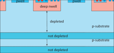
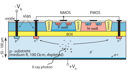
HVCMOS prototypes have been tested to TIDs well above 100 Mrad and fluences up to 51015 neq/cm2 [185]. The most critical performance metric is the so-called in-time efficiency of hits after irradiation which includes both radiation damage characterizations as well as rate demands at the LHC. The term in-time means that a hit must be time-stamped within one LHC bunch-crossing window of 25 ns. Test beam characterization of prototype matrices coupled to the FE-I4 pixel chip via adhesive bonding yielded efficiencies of above 97% (99.7% up to 11015neq cm-2) and in-time efficiencies comparable to those of FE-I4 hybrid pixel modules used in the same test beam (95% within three beam bunch crossings of 25 ns) [185].
Prototype matrices were tested up to fluences of 11015neq cm-2) and TIDs of 50 Mrad [27] using an approach that differs from the above mainly in two aspects, (i) use of a quadruple well 150 nm process (LFoundry LF15A) as in fig. 40(b), and (ii) use of high resistivity substrate wafers (2–3 kcm). This technology allows for bias voltages in the 150–200 V range. The devices performed well in test beams, showing high time integrated efficiencies, but not yet with fast enough timing (1 bunch crossing in-time efficiency 91%) owing to the large capacitance inherent in the large fill-factor approach. The depletion depth of these devices has been measured for increasing radiation fluence [181] (up to 8neq cm-2, fig. 45) using edge TCT (transient current technique, see for example [186]), which measures the transient current generated by a laser pulse parallel to the CMOS sensor surface, entering the bulk through a diced edge. As a function of bias voltage, the square root shape of eq. (16) is observed, clearly showing that depletion depth values of 30–50 m are maintained even for fluences beyond 1015neq cm-2.
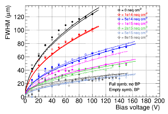
CMOS on SOI
The SOI technology provides a buried oxide layer (BOX) separating the CMOS electronics from the substrate layer. Both parts are connected by vertical via structures reaching through the BOX and leading to an n-implant which acts as the charge collecting node. Monolithic SOI-based pixel structures have been developed for some time using the fully depleted (FD) SOI technology [189], invented for high speed CMOS electronics with reduced (parasitic) capacitances. The CMOS electronics layer is embedded in depleted silicon. The developments in this FD-SOI technology, however suffer from effects inherent to the BOX oxide layer, most notably the so-called back-gate effect and from radiation effects [189] that can be compensated to some degree [190] for moderate radiation doses, but not for the radiation conditions expected at the HL-LHC.
Thick film SOI, however, featuring trench isolation and doped, only partially depleted regions underneath CMOS transistors, thus shielding the transistors (cf. fig. 44(b)), is free of these difficulties and can also sustain much larger radiation doses. SOI CMOS pixel detectors have been realised [191] and characterised [192] in the lab and in test beams. The devices show impressive TID tolerances tested up to 1 Grad. Also here the substrate resistivity initially increases with hadron fluence due to acceptor removal. The measured in-time efficiency also needs modest improvement in order to cope with LHC demands.
While the CMOS on SOI approach towards monolithic pixel detectors remains very interesting, not the least because of the attractive approach of separating sensing and electronics volume by a buried oxide layer, it is currently not the main focus of the HL-LHC developments.
DMAPS with small fill-factor
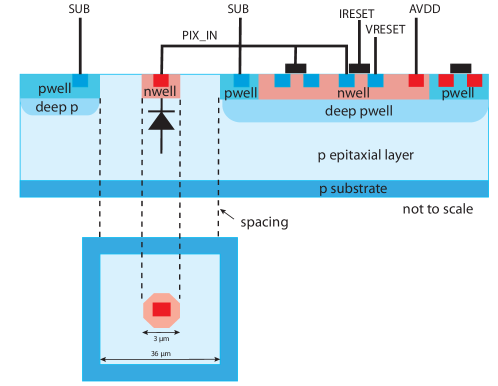
A recent development aims to achieve sufficient radiation hardness with a small fill-factor design, promising low noise and fast timing due to the small resulting input capacitance. The development inherits from the design of the ALICE ITS pixel chip (ALPIDE) development [194, 177] introducing some technology improvements for better charge collection after irradiation [195]. Figure 46 shows a principal cell layout. The charge collection is obtained in a high ohmic ( 1 kcm) epitaxial layer. The quadruple well features are very similar to those in fig. 40(b). The main difference is the layout of the charge collection node placed far outside the electronics area with minimal geometric size. The capacitance is very low: 3–10 fF [196], depending on the geometry and pitch of the collection node. The pixel area must be small (m) in order to limit the maximum path length for charge collection.
In a first prototype chip (TJ Investigator) the main features of such a design have been investigated [193] confirming the low capacitance and the good timing precision ( ns). To obtain a fully depleted volume the TJ process was modified replacing the epitaxial p-layer by a planar deep n+-p junction [193]. A fully monolithic chip including readout architecture has been recently submitted for fabrication with expected noise figures of 16–20 e- and similar timing precision.
6.3 Outlook on DMAPS pixels
The development of depleted CMOS active pixels currently has a large momentum in the high energy physics community. Many groups are active in developing DMAPS sensors and also DMAPS based modules. The specific developments discussed above are not an exhaustive survey and we are aware of other manufacturers and competing efforts that have not yet published results. Significant new material is therefore expected within 1 year of this review. Whether the development can be brought to a level of maturity sufficient to be adopted for (parts of) an HL-LHC pixel detectors remains to be seen. Regardless of the outcome for HL-LHC, researchers in this field expect that CMOS active pixels will be the preferred technology for future, large area, high rate and radiation trackers
7 Summary and conclusions
With the planned high luminosity upgrades of the LHC machine and experiments, pixel detectors operating in high rate and radiation environments are facing yet another extreme challenge, surpassing that of the current LHC by roughly an order of magnitude. While integrated (monolithic) pixel detectors have been developed already for some time (and are in fact used in detectors under less hostile experimental conditions), as of today hybrid pixel detectors still constitute the state of the art in tracking detector technology close to the interaction point of such high rate and radiation experiments.
In this paper we have reviewed the fundamentals of track space-time point and direction measurements and described development routes and choices to be made for the next generation HL-LHC experiments. These address all components of the hybrid pixel technology, most prominently the sensor and the readout chip, but also interconnection and 3D-stacking techniques, and lightweight support and cooling structures. Beyond the traditional space point measurement, ways to extract and use additional information from pixel detectors are being explored, such as space vector information or precision timing information with the promise of so-called 4D tracking.
Silicon sensors capable of good performance after fluences of neqcm-2 and beyond have been developed (sections 3.1 and 3.2). Both 3D-Si sensors and conventional planar sensors have been shown to be able to cope with the demands. 3-D sensors after further optimization following their successful performance in the IBL pixel upgrade of ATLAS [197], and planar sensors after reducing thickness and optimizing guard ring structures.
A major challenge is the development of a next generation of pixel readout chips which must cope with very harsh radiation conditions (total doses up to 1 Grad), with particle rates GHz/cm2, and with MHz trigger rates leading to data output bandwidths of (10 Gb/s). The development of a close to 109 transistor readout chip is jointly addressed by ATLAS and CMS through the RD53 collaboration [30] using deep submicron 65 nm technology. Narrow and short transistor channel effects lead to complex radiation damage behavior that demands sophisticated modelling to be properly addressed (section 4.4). An approach dubbed 'analog islands in a digital sea' is employed to process the very large rates on chip. The RD53 chip will serve as the workhorse for the HL-LHC hybrid pixel detectors of the experiments.
Advances in evaporative cooling and in using lightweight yet stiff composite materials render possible a material budget reduction per pixel layer from previously above 3% to below 1%, even for power and cooling intensive high rate and radiation applications (chapter 5). Coolant choices have narrowed down to CO2 as today’s state of the art. Very small diameter pipes (micro channels) are an attractive development path for high cooling capacity.
Finally, the monolithic pixel module ansatz is being revived by employing multiple well technologies on high resistivity substrates that have become more commercially accessible to the HEP community and now offer good performance even under HL-LHC requirements (chapter 6). This has also launched R&D using CMOS technology lines for (passive) sensors in hybrid pixel detectors (section 3.1), offering advantages as low cost, capacitive coupling of electrodes as well as efficient routing between sensor and ROIC pixels by exploiting CMOS metal layers.
Acknowledgements
The authors are grateful to many colleagues for their excellent published work and ideas, and for many discussions and other contributions. This work was supported by the Office of High Energy Physics of the U.S. Department of Energy under contract DE-AC02-05CH11231, by the Deutsche Forschungsgemeinschaft DFG, grant number WE 976/4-1, and by the German Ministry for Research BMBF under grant number 05H15PDCA9.
References
- [1] L. Rossi, P. Fischer, T. Rohe, and N. Wermes. Pixel Detectors: From Fundamentals to Applications. Springer, Berlin, Heidelberg, 2006.
- [2] M. Moll. Displacement damage in silicon detectors for High Energy Physics. In Proceedings of Radecs 2017, Geneva, Switzerland, Oct. 2017. to appear in IEEE Trans. Nucl. Sci.
- [3] G. Viehhauser. Thermal management and mechanical structures for silicon detector systems. JINST, 10(09):P09001, 2015.
- [4] G. Aad et al. ATLAS pixel detector electronics and sensors. JINST, 3:P07007, 2008.
- [5] F. Hügging. The ATLAS Pixel Insertable B-Layer (IBL). Nucl. Instr. and Meth. A, 650:45–49, 2011.
- [6] M. Garcia-Sciveres et al. The FE-I4 pixel readout integrated circuit. Nucl. Instr. and Meth. A, 636:155, 2011.
- [7] H.C. Kastli et al. CMS barrel pixel detector overview. Nucl. Instr. and Meth. A, 582:724, 2007.
- [8] A. Dominguez et al. CMS Technical Design Report for the Pixel Detector Upgrade. Technical Report CERN-LHCC-2012-016, CMS-TDR-11, 2012.
- [9] D. Hits and A. Starodumov. The CMS Pixel Readout Chip for the Phase 1 Upgrade. JINST, 10(05):C05029, 2015.
- [10] A. Affolder et al. DC-DC converters with reduced mass for trackers at the HL-LHC. JINST, 6(11):C11035, 2011.
- [11] P. Collins et al. LHCb VELO Upgrade Technical Design Report. Technical Report CERN-LHCC-2013-021, LHCB-TDR-013, 2013.
- [12] T. Poikela et al. VeloPix: the pixel ASIC for the LHCb upgrade. JINST, 10(01):C01057, 2015.
- [13] G. Aglieri Rinella et al. The NA62 GigaTracker. Nucl. Instrum. Meth., A845:147–149, 2017.
- [14] ATLAS Collaboration. The optimization of ATLAS track reconstruction in dense environments. ATLAS note: ATL-PHYS-PUB-2015-006, CERN 2015.
- [15] R.L. Gluckstern. Uncertainties in track momentum and direction, due to multiple scattering and measurement errors. Nucl. Instr. and Meth., 24:381, 1963.
- [16] K.A. Olive et al. Review of Particle Physics (RPP). Chin. Phys., C38:090001, 2014. An updated RPP is published every 2 years. The online access to the current and previous issues is available from http://pdg.lbl.gov/.
- [17] V. Bartsch et al. Lorentz angle measurements in silicon detectors. Nucl. Instr. and Meth. A, A478:330–332, 2002.
- [18] T. Hemperek et al. Digital Architecture of the New ATLAS Pixel Chip FE-I4. In Proceedings, 2009 IEEE Nuclear Science Symposium and Medical Imaging Conference (NSS/MIC 2009), pages 791–796, 2009.
- [19] H. Kolanoski and N. Wermes. Teilchendetektoren: Grundlagen und Anwendungen. Springer, Berlin, Heidelberg, New York, 2016.
- [20] P. Fischer. Comments on the reconstruction of hit positions in segmented detectors. private communication, to be published in JINST, 2015.
- [21] E. Belau et al. Charge collection in silicon strip detectors. Nucl. Instr. and Meth., 214:253, 1983.
- [22] R. Turchetta. Spatial resolution of silicon microstrip detectors. Nucl. Instr. and Meth. A, 335:44–58, 1993.
- [23] ATLAS Collaboration. IBL Efficiency and Single Point Resolution in Collision Events. Technical Report ATL-INDET-PUB-2016-001, CERN, Geneva, Aug 2016.
- [24] S. Chatrchyan et al. Description and performance of track and primary-vertex reconstruction with the CMS tracker. JINST, 9(10):P10009, 2014.
- [25] P. Soussan, B. Majeed, P. Le Boterf, and P. Bouillon. Development and Evaluation of Lead Free Reflow Soldering Techniques for the Flip Chip Bonding of Large GaAs Pixel Detectors on Si Readout Chip. In Proc. EPTC 2014, the 16th Electronic Packaging and Technology Conference, pages 453–457, Orlando, USA, 2014.
- [26] I. Peric et al. High-voltage pixel sensors for ATLAS upgrade. Nucl. Instr. and Meth. A, 765:172–176, 2014.
- [27] T. Hirono et al. Characterization of Fully Depleted CMOS Active Pixel Sensors on High Resistivity Substrates for Use in a High Radiation Environment. 2016. preprint arXiv:1612.03154 [physics.ins-det], 2016.
- [28] A. Miucci et al. Radiation-hard Active Pixel Sensors for HL-LHC Detector Upgrades based on HV-CMOS Technology. JINST, 9:C05064, 2014.
- [29] H. Spieler. Semiconductor Detector Systems. Oxford University Press, 2005.
- [30] RD53 Collaboration. RD53A Integrated Circuit Specifications. Technical Report CERN-RD53-PUB-15-001, 2015.
- [31] H. F. W. Sadrozinski et al. Ultra-fast silicon detectors. Nucl. Instr. and Meth., A730:226–231, 2013.
- [32] N. Cartiglia et al. Performance of Ultra-Fast Silicon Detectors. JINST, 9:C02001, 2014. arXiv:1312.1080 [physics.ins-det], 2013.
- [33] N. Cartiglia et al. Tracking in 4 dimensions. Nucl. Instrum. Meth., A845:47–51, 2017.
- [34] P. Buzhan et al. An advanced study of silicon photomultiplier. ICFA Instrum. Bull., 23:28–41, 2001.
- [35] P. Buzhan et al. Silicon photomultiplier and its possible applications. Nucl. Instr. and Meth. A, 504:48–52, 2003.
- [36] T. Stokes. Avalanche Photodiodes: Theory and Applications, Hamamatsu, 2005. weblink http://www.photonicsonline.com/doc/avalanche-photodiodes-theory-and-applications-0001.
- [37] W. Riegler and C. Lippmann. The physics of resistive plate chambers. Nucl. Instr. and Meth. A, 518:86–90, 2004.
- [38] N. Cartiglia et al. Design optimization of ultra-fast silicon detectors. Nucl. Instr. and Meth., A796:141–148, 2015.
- [39] F. Cenna et al. Weightfield2: A fast simulator for silicon and diamond solid state detectors. Nucl. Instr. and Meth., A796:149–153, 2015.
- [40] A. Shockley. Currents to conductors induced by a moving point charge. J. Appl. Phys., 9:635, 1938.
- [41] S. Ramo. Currents induced by electron motion. Proceedings of the I.R.E, 27:584–585, 1939.
- [42] N. Cartiglia et al. The 4D pixel challenge. JINST, 11(12):C12016, 2016.
- [43] H.F.-W. Sadrozinski et al. Ultra-fast silicon detectors (UFSD). Nucl. Instr. and Meth. A, 831:18–23, 2016.
- [44] N. Cartiglia et al. Beam test results of a 16 ps timing system based on ultra-fast silicon detectors. Nucl. Instrum. Meth., A850:83–88, 2017. preprint arXiv:1608.08681 [physics.ins-det], 2016.
- [45] RD50 Collaboration. CERN. https://rd50.web.cern.ch/rd50.
- [46] M. Mannelli, R. Pöschl, and A. Seiden. Energy and time measurements with high-granular silicon devices. 2017. preprint arXiv:1704.01304 [physics.ins-det], 2017.
- [47] R. Arcidiacono et al. Test of UFSD Silicon Detectors for the TOTEM Upgrade Project. 2017. preprint arXiv:1702.05180 [physics.ins-det], 2017.
- [48] G. Lindstrom et al. Radiation hard silicon detectors – Developments by the RD48 (ROSE) Collaboration. Nucl. Instr. and Meth. A, 466:308–326, 2001.
- [49] J. Harkonen et al. Radiation hardness of Czochralski silicon, float zone silicon and oxygenated float zone silicon studied by low energy protons. Nucl. Instr. and Meth. A, 518:346–348, 2004.
- [50] I. Pintilie, G. Lindstroem, A. Junkes, and E. Fretwurst. Radiation-induced point- and cluster-related defects with strong impact on damage properties of silicon detectors. Nucl. Instr. and Meth. A, 611:52–68, 2009.
- [51] C. Kenney, S. Parker, and J. Segal. 3d - a proposed new architecture for solid-state radiation detectors. Nucl. Instr. and Meth. A, 395:328–343, 1997.
- [52] A. Macchiolo, R. Nisius, N. Savic, and S. Terzo. Development of n-in-p pixel modules for the ATLAS Upgrade at HL-LHC. Nucl. Instr. and Meth., A831:111–115, 2016.
- [53] A. Macchiolo. Thin planar silicon sensors. private communication, 2016.
- [54] S. Terzo, L. Andricek, A. Macchiolo, H. G. Moser, R. Nisius, R. H. Richter, and P. Weigell. Heavily Irradiated N-in-p Thin Planar Pixel Sensors with and without Active Edges. JINST, 9:C05023, 2014.
- [55] S. Terzo. Development of radiation hard pixel modules employing planar n-in-p silicon sensors with active edges for the ATLAS detector at HL-LHC. PhD thesis, TU Munich, 2015. https://publications.mppmu.mpg.de/2015/MPP-2015-291/FullText.pdf.
- [56] M. Dragicevic et al. Results from a beam test of silicon strip sensors manufactured by Infineon Technologies AG. Nucl. Instr. and Meth., A765:1–6, 2014.
- [57] T. Bergauer, M. Dragicevic, A. König, J. Hacker, and U. Bartl. First thin AC-coupled silicon strip sensors on 8-inch wafers. Nucl. Instr. and Meth., A830:473–479, 2016.
- [58] R.D. Schinella, and K. Chao. Use of reticle stitching to provide design flexibility, July 1997. US Patent 5,652,163.
- [59] L.F. Miller (IBM). Controlled Collapse Reflow Chip Joining. J. Res. Dev., 13:239–250, 1969.
- [60] D. L. Pohl, T. Hemperek, F. Hügging, J. Janssen, H. Krüger, A. Macchiolo, N. Owtscharenko, I. Caicedo Sierra, L. Vigani, and N. Wermes. Radiation hard pixel sensors using high-resistive wafers in a 150 nm CMOS processing line. 2017. preprint arXiv:1702.04953 [physics.ins-det], 2017.
- [61] C. Da Via et al. 3D active edge silicon sensors: Device processing, yield and QA for the ATLAS-IBL production. Nucl. Instr. and Meth. A, 699:18–21, 2013.
- [62] C. Da Via et al. 3D silicon detectors status and applications. Nucl. Instr. and Meth. A, 549:122–125, 2005.
- [63] G. Pellegrini et al. 3D double sided detector fabrication at IMB-CNM. Nucl. Instr. and Meth. A, A699:27–30, 2013.
- [64] G. Giacomini, A. Bagolini, M. Boscardin, et al. Development of Double-Sided Full-Passing-Column 3D Sensors at FBK. IEEE Trans. Nucl. Sci., 60:2357–2366, 2013.
- [65] G.-F. Dalla Betta et al. 3D silicon sensors: irradiation results. PoS, Vertex2012:014, 2013.
- [66] G. Pellegrini et al. First double-sided 3-D detectors fabricated at CNM-IMB. Nucl. Instr. and Meth., A592:38–43, 2008.
- [67] G-F. Dalla Betta et al. Development of a new generation of 3D pixel sensors for HL-LHC. Nucl. Instr. and Meth., A824:386–387, 2016.
- [68] A. La Rosa. The ATLAS Insertable B-Layer: from construction to operation. JINST, 11(12):C12036, 2016.
- [69] J. Lange et al. 3D silicon pixel detectors for the High-Luminosity LHC. JINST, 11(11):C11024, 2016.
- [70] G.-F. Dalla Betta et al. Development of a new generation of 3D pixel sensors for HL-LHC. Nucl. Instrum. Meth., A824:386–387, 2016.
- [71] G.-F. Dalla Betta et al. Development of New 3D Pixel Sensors for Phase 2 Upgrades at LHC. 2016. http://inspirehep.net/record/1501528/files/arXiv:1612.00608.pdf.
- [72] G.-F. Dalla Betta. 3D-Si sensor design. private communication, 2017.
- [73] D.M.S. Sultan et al. First Production of New Thin 3D Sensors for HL-LHC at FBK. In Proceedings, 18th International Workshop on Radiation Imaging Detectors (IWORID 2016): Barcelona, Spain, July 3-7, 2016, 2016.
- [74] J. Lange. 3D-Si sensor design. private communication, 2017.
- [75] P. Ramm et al. Handbook of Wafer Bonding. Wiley-VCH, Weinheim, Germany, 2012.
- [76] P. Garrou, C. Bower, and P. Ramm, editors. Handbook of 3D Integration, volume 1&2. Wiley-VCH, Weinheim, Germany, 2012.
- [77] P. Garrou, M. Koyanagi, and P. Ramm, editors. Handbook of 3D Integration, volume 3. Wiley-VCH, Weinheim, Germany, 2014.
- [78] H. Oppermann and M. Hutter. Au/Sn solder. In Handbook of Wafer Bonding, P. Ramm, J-Q. Lu, M.M.V. Taklo (eds.), pages 119–138, Weinheim, Germany, 2012. Wiley-VCH.
- [79] L. Dietrich, M. Töpper, Th. Fritzsch, O. Ehrmann, and H. Reichl. Prospects and Yield of Electrochemical Wafer Plating for Bumping and Signal Routing. In Proc. EMPC 2007, the 16th European Microelectronics and Packaging Conference, pages 458–466, Oulu, Finland, 2007.
- [80] M. Klein et al. Development and Evaluation of Lead Free Reflow Soldering Techniques for the Flip Chip Bonding of Large GaAs Pixel Dedectors on Si Readout Chip. In Proc. ECTC 2008, the 58th Electronic Components and Technology Conference, pages 1893–1899, Orlando, USA, 2008.
- [81] Ch. Broennimann et al. Development of an indium bump bond process for silicon pixel detectors at PSI. Nucl. Instrum. Meth., A565:303–308, 2006.
- [82] G. Alimonti et al. Pixel Hybridization Technologies for the HL-LHC. JINST, 11(12):C12077, 2016.
- [83] A. Munding et al. Cu/Sn solid liquid interdiffusion bonding. In Wafer Level 3-D ICs Process Technology, pages 131–170. Springer Science, N.Y., 2008.
- [84] R. Patti. 3D Integration at Tezzaron Semiconductor Corporation, pages 463–486. Wiley-VCH Verlag GmbH & Co. KGaA, 2008.
- [85] Internationl Roadmap Committee. The International Technology Roadmap for Semiconductors (ITRS). 2011 Edition. Semiconductor Industry Association, 2011.
- [86] F. Laermer and A. Schilp. Method for anisotropic plasma etching of substrates. US Patent, 5,498,312, 1996.
- [87] M.J. Wolf. Through Silicon Vias. private communication, 2017.
- [88] T. Fritzsch. Straight through silicon vias. private communication, 2017.
- [89] M. Barbero et al. A via last TSV process applied to ATLAS pixel detector modules: proof of principle demonstration. JINST, 7(08):P08008, 2012.
- [90] M. Sarajlic et al. Development of edgeless tsv x-ray detectors. JINST, 11(02):C02043, 2016.
- [91] N. Wermes et al. TSVs in FE-I4. In Presentation at the AIDA-2020 Annual Meeting, Hamburg, Germany, 2016.
- [92] S. Kühn et al. Compact Pixel module with through-silicon vias. In IEEE NSS/MIC Conference, Strasbourg, France, 2016.
- [93] CEA/LETI. private communication, 2017.
- [94] E. Heijne and P. Jarron. Development of silicon pixel detectors: An introduction. Nucl. Instr. and Meth. A, 275:467–471, 1989.
- [95] I. Peric et al. The FEI3 readout chip for the ATLAS pixel detector. Nucl. Instr. and Meth. A, 565:178–187, 2006.
- [96] M. Barbero et al. Design and test of the CMS pixel readout chip. Nucl. Instr. and Meth. A, 517:349–359, 2004.
- [97] X. Llopart and M. Campbell. First test measurements of a 64k pixel readout chip working in single photon counting mode. Nucl. Instr. and Meth. A, 509(1-3):157–163, 2003.
- [98] R. Ballabriga et al. The Medipix3RX: a high resolution, zero dead-time pixel detector readout chip allowing spectroscopic imaging. JINST, 8(02):C02016, 2013.
- [99] T. Poikela et al. Timepix3: a 65K channel hybrid pixel readout chip with simultaneous ToA/ToT and sparse readout. JINST, 9(05):C05013, 2014.
- [100] P. P Valerio et al. A prototype hybrid pixel detector ASIC for the CLIC experiment. JINST, 9(01):C01012, 2014.
- [101] M. Campbell et al. Towards a new generation of pixel detector readout chips. JINST, 11(01):C01007, 2016.
- [102] Z. Or-Bach. EETimes: Intel Calls for 3D IC, 2015. http://www.eetimes.com/author.asp?doc_id=1325921.
- [103] R. Merrit. EETimes: Chip Stacks at 30,000 Feet, 2015. http://www.eetimes.com/author.asp?doc_id=1326936.
- [104] G. Deptuch et al. VIPIC IC—Design and test aspects of the 3D pixel chip. In IEEE Nucl. Sci. Symp. Conf. Rec.: 1540-1543, 2010, pages 1540–1543, Orlando, FL, USA, 2010.
- [105] G. Deptuch et al. Fully 3-D Integrated Pixel Detectors for X-Rays. IEEE Trans. Electron Devices, 63(1):205–214, 2016.
- [106] R. Nowlin et al. A New Total-Dose-Induced Parasitic Effect in Enclosed-Geometry Transistors. IEEE Trans. Nucl. Sci., 52(6):2495–2502, 2005.
- [107] Radu R. et al. Investigation of point and extended defects in electron irradiated silicon—Dependence on the particle energy. Journal of Applied Physics, 117:164503, 2015.
- [108] S. S. Mattiazzo et al. Total Ionizing Dose effects on a 28 nm Hi-K metal-gate CMOS technology up to 1 Grad. JINST, 12(02):C02003, 2017.
- [109] A.S. Grove et al. MOS C-V Model. Solid State Elect., 8:145, 1965.
- [110] F. Faccio and G. Cervelli. Radiation induced edge effects in deep submicron CMOS transistors. IEEE Trans. Nucl. Sci., 52(6):2413–2420, 2005.
- [111] F. Faccio et al. Radiation-Induced Short Channel (RISCE) and Narrow Channel (RINCE) Effects in 65 and 130 nm MOSFETs. IEEE Trans. Nucl. Sci., 62(6), 2015.
- [112] K. Dette. Total Ionising Dose effects in the FE-I4 front-end chip of the ATLAS Pixel IBL detector. JINST, 11(11):C11028, 2016.
- [113] M. Backhaus. Parametrization of the radiation induced leakage current increase of NMOS transistors. JINST, 12(01):P01011, 2017.
- [114] M. Menouni et al. 1-Grad total dose evaluation of 65 nm CMOS technology for the HL-LHC upgrades. JINST, 10(05):C05009, 2015.
- [115] P. Roche et al. A Commercial 65 nm CMOS Technology for Space Applications: Heavy Ion, Proton and Gamma Test Results and Modeling. IEEE Trans. Nucl. Sci., 57(4):2079–2088, 2010.
- [116] M. Menouni et al. Design and measurements of SEU tolerant latches. In Electronics for particle physics. Proceedings, Topical Workshop, TWEPP-08, Naxos, Greece, 15-19 September 2008, pages 402–405, 2008.
- [117] T. Calin, M. Nicolaidis, and R. Velazco. Upset hardened memory design for submicron CMOS technology. IEEE Trans. Nucl. Sci., 43(6):2874–2878, 1996.
- [118] O. Amusan et al. Single Event Upsets in a 130 nm Hardened Latch Design Due to Charge Sharing. In 45th annual IEEE international Reliability physics symposium, proceedings., 2007.
- [119] M. Menouni. private communication, to be published, 2017.
- [120] M Manghisoni et al. 130 and 90 nm CMOS technologies for detector front-end applications. Nucl. Instr. and Meth. A, 572(1):368 – 370, 2007.
- [121] F. Fahim. Fermi CMS Pixel (FCP130) test ASIC. Technical Report FERMILAB-CONF-14-435-PPD, 2014.
- [122] E. Martin et al. The 5ns peaking time transimpedance front end amplifier for the silicon pixel detector in the NA62 Gigatracker. In Nucl. Sci. Symposium Conf. Record (NSS/MIC), 2009 IEEE. IEEE, 2010.
- [123] R. Carney et al. Results of FE65-P2 Pixel Readout Test Chip for High Luminosity LHC Upgrades. In Proc. 38th International Conference on High Energy Physics, ICHEP2016, page 272, Chicago, USA, 2016.
- [124] E. Monteil et al. A prototype of a new generation readout ASIC in 65nm CMOS for pixel detectors at HL-LHC. JINST, 11(12):C12044, 2016.
- [125] T. Heim and M. Garcia-Sciveres. Self-Adjusting Threshold Mechanism for Pixel Detectors. 2017. To appear in Nucl. Inst. and Meth. A.
- [126] D.G. Kendall. Stochastic Processes Occurring in the Theory of Queues and their Analysis by the Method of the Imbedded Markov Chain. The Annals of Mathematical Statistics, 24(3):338, 1953.
- [127] L. Gaioni, F. De Canio, M. Manghisoni, L. Ratti, V. Re, and G. Traversi. 65 nm CMOS analog front-end for pixel detectors at the HL-LHC. JINST, 11(02):C02049, 2016.
- [128] M. Garcia-Sciveres and X. Wang. Data encoding efficiency in pixel detector readout with charge information. Nucl. Instr. and Meth. A, 815:18 – 22, 2016.
- [129] J. Proakis and M. Salehi. Digital Communications. McGraw Hill, 2000.
- [130] V. Wallängen and M. Garcia-Sciveres. Decision feedback equalization for radiation hard data link at 5 Gbps. JINST, 12(01):C01067, 2017.
- [131] R. Bates et al. High speed electrical transmission line design and characterization. JINST, 12(02):C02002, 2017.
- [132] N. McFadden, M. Hoeferkamp, and S. Seidel. Radiation-tolerant, low-mass, high bandwidth, flexible printed circuit cables for particle physics experiments. Nucl. Instr. and Meth. A, A830:461–465, 2016.
- [133] J. Shahinian et al. High speed data transmission on small gauge cables for the ATLAS Phase-II Pixel detector upgrade. JINST, 11(03):C03024, 2016.
- [134] ATLAS Collaboration. ATLAS pixel detector: Technical Design Report. Technical Report ATLAS-TDR-11, CERN-LHCC-98-013, 1998.
- [135] D. Hall, T. Huffman, and A. Weidberg. The radiation induced attenuation of optical fibres below -20∘C exposed to lifetime HL-LHC doses at a dose rate of 700 Gy(Si)/hr. JINST, 7(01):C01047, 2012.
- [136] G. G Mazza et al. The GBLD: a radiation tolerant laser driver for high energy physics applications. JINST, 8(01):C01033, 2013.
- [137] S. Seif El Nasr-Storey et al. Effect of Radiation on a Mach-Zehnder Interferometer Silicon Modulator for HL-LHC Data Transmission Applications. IEEE Trans. Nucl. Sci., 62(1):329–335, 2015.
- [138] S. Michelis et al. Inductor based switching DC-DC converter for low voltage power distribution in SLHC. In Proc. Electronics for Particle Physics, 2007.
- [139] F. Faccio et al. FEAST2: A Radiation and Magnetic Field Tolerant Point-of-Load Buck DC/DC Converter. In Radiation Effects Data Workshop (REDW), 2014 IEEE, 2015.
- [140] C.Y. Lui et al. Design and modeling of the step-down piezo transformer. In Proc. Euro. Particle Accelerator Conf., page 26, 2006.
- [141] P. Denes et al. A Capacitor Charge Pump DC-DC Converter for Physics Instrumentation. IEEE Trans. Nucl. Sci., 56(3):1507, 2009.
- [142] A. Krieger et al. Design of Fully-Integrated DC-DC Converters for High Energy Physics Applications. Presented at IEEE NSS/MIC, Seattle, 2014.
- [143] J. Chesnoy, editor. Undersea Fiber Communication Systems. Elsevier, 2015.
- [144] T. Stockmanns et al. Serial powering of pixel modules. Nucl. Instr. and Meth. A, 511:174–179, 2003.
- [145] D.B. Ta et al. Serial powering: Proof of principle demonstration of a scheme for the operation of a large pixel detector at the LHC. Nucl. Instr. and Meth. A, 557:445–459, 2006.
- [146] V. Filimonov et al. A serial powering pixel stave prototype for the ATLAS ITk upgrade. JINST, 12(03):C03045, 2017.
- [147] J. Matheson. Progress and advances in serial powering of silicon modules for the atlas tracker upgrade. JINST, 6(01):C01019, 2011.
- [148] M. Karagounis et al. An integrated Shunt-LDO regulator for serial powered systems. In Proceedings of ESSCIRC ’09, 2009.
- [149] C.M. Zhang et al. GigaRad Total Ionizing Dose and Post-Irradiation Effects on 28 nm Bulk MOSFETs. In IEEE Nuclear Science Symposium. IEEE, 2016.
- [150] ATLAS Collaboration. Studies of the ATLAS Inner Detector material using 13 TeV collision data. Technical Report ATL-PHYS-PUB-2015-050, CERN, Geneva, Nov 2015.
- [151] ATLAS Collaboration. ATLAS Insertable B-Layer: Technical Design Report. Technical Report ATLAS-TDR-19, CERN-LHCC-2010-013, 2010.
- [152] B Abelev et al. Technical Design Report for the Upgrade of the ALICE Inner Tracking System. J. Phys., G41:087002, 2014.
- [153] J. Schambach et al. The STAR Heavy Flavor Tracker (HFT). In Proceedings, 20th International Conference on Particles and Nuclei (PANIC 14): Hamburg, Germany, August 24-29, 2014, pages 659–664, 2014.
- [154] H. Wieman et al. STAR PIXEL detector mechanical design. JINST, 4(05):P05015, 2009.
- [155] A. Delil, A. Woering, and B. Verlaat. Development of a Mechanically Pumped Two-Phase CO2 Cooling Loop for the AMS-2 Tracker Experiment. In SAE Technical Paper. SAE International, 07 2002.
- [156] B. Verlaat and A-P. Colijn. CO2 cooling developments for HEP detectors. PoS, VERTEX2009:031, 2009.
- [157] D. Attree et al. The evaporative cooling system for the ATLAS inner detector. JINST, 3(07):P07003, 2008.
- [158] M. Garcia-Sciveres. Post-installation status of the ATLAS pixel detector. JINST, 4(03):P03021, 2009.
- [159] G. Romagnoli et al. Silicon micro-fluidic cooling for NA62 GTK pixel detectors. Microelectronic Engineering, 145:133 – 137, 2015.
- [160] O. de Aguiar Francisco et al. Evaporative CO2 microchannel cooling for the LHCb VELO pixel upgrade. JINST, 10(05):C05014, 2015.
- [161] T. Kohriki et al. First observation of thermal runaway in the radiation damaged silicon detector. IEEE Trans. Nucl. Sci., 43(3):1200–1202, 1996.
- [162] A. Sharma. The Phase-II ATLAS Pixel Tracker Upgrade: Layout and Mechanics. In Proceedings, IEEE Nuclear Science Symposium and Medical Imaging Conference, Strasbourg, France, 29 Oct 2016, 2017.
- [163] W. Miller et al. Allcomp, inc., 2017. http://http://www.allcomp.net/.
- [164] A. Pepato et al. The mechanics and cooling system of the ALICE silicon pixel detector. Nucl. Instr. and Meth. A, 565:6–12, 2006.
- [165] N. Hartman et al. Novel fabrication techniques for low-mass composite structures in silicon particle detectors. Nucl. Instr. and Meth. A, 732:103–108, 2013.
- [166] B. Smart. ATLAS pixel detector design for the HL-LHC. JINST, 12(02):C02011, 2017.
- [167] P Delebecque et al. Alpine Pixel Detector Layout. Technical Report ATL-UPGRADE-PUB-2013-009, CERN, Geneva, Feb 2013.
- [168] E. Migliore. CMS Pixel Detector design for HL-LHC. JINST, 11(12):C12061, 2016.
- [169] ATLAS Phase-II Upgrade Scoping Document. Technical Report CERN-LHCC-2015-020. LHCC-G-166, CERN, Geneva, Sep 2015.
- [170] D. Whiteson et al. Observing Ultra-High Energy Cosmic Rays with Smartphones. 2015. arXiv:1410.2895.
- [171] Sherwood Parker. A proposed vlsi pixel device for particle detection. Nucl. Instr. and Meth. A, 275(3):494 – 516, 1989.
- [172] C.J. Kenney, S.I. Parker, V.Z. Peterson, W.J. Snoeys, J.D. Plummer, and C. H. Aw. A prototype monolithic pixel detector. Nucl. Instr. and Meth. A, 342(1):59 – 77, 1994.
- [173] B. Dierickx, G. Meynants, and D. Scheffer. Near 100 fill factor CMOS active pixel. In Proc. SPIE – Int. Soc. Opt. Eng. (USA), volume 3410, pages 68–76, 1998.
- [174] R. Turchetta et al. A monolithic active pixel sensor for charged particle tracking and imaging using standard VLSI CMOS technology. Nucl. Instr. and Meth. A, 458:677–689, 2001.
- [175] G. Contin et al. The MAPS-based vertex detector for the STAR experiment: Lessons learned and performance. Nucl. Instr. and Meth. A, 831:7–11, 2016.
- [176] J. Schambach et al. A MAPS Based Micro-Vertex Detector for the STAR Experiment. In Physics Procedia, volume 66, pages 514–519, 2015.
- [177] M. Mager. ALPIDE, the Monolithic Active Pixel Sensor for the ALICE ITS upgrade. Nucl. Instrum. Meth., A824:434–438, 2016.
- [178] N. Wermes. Depleted CMOS pixels for LHC proton-proton experiments. Nucl. Instr. and Meth. A, A824:483–486, 2016.
- [179] M. Havranek, F. Hügging, H. Krüger, and N. Wermes. Measurement of pixel sensor capacitances with sub-femtofarad precision. Nucl. Instr. and Meth. A, 714:83–89, 2013.
- [180] E. Andersen. Cooling of pixel support structures. private communication, 2016.
- [181] Igor Mandic et al. Neutron irradiation test of depleted CMOS pixel detector prototypes. JINST, 12(02):P02021, 2017.
- [182] M. Havránek et al. DMAPS: a fully depleted monolithic active pixel sensor—analog performance characterization. JINST, 10(02):P02013, 2015.
- [183] I. Peric, C. Kreidl, and P. Fischer. Hybrid pixel detector based on capacitive chip to chip signal-transmission. Nucl. Instrum. Meth., A617:576–581, 2010.
- [184] I. Peric. A novel monolithic pixelated particle detector implemented in high-voltage CMOS technology. Nucl. Instr. and Meth. A, 582:876–885, 2007.
- [185] M. Benoit et al. Testbeam results of irradiated AMS H18 HV-CMOS pixel sensor prototypes. 2016. preprint arXiv:1611.02669 [physics.ins-det], 2016.
- [186] G. Kramberger et al. Investigation of electric field and charge multiplication in silicon detectors by Edge-TCT. In Proceedings, 2009 IEEE Nuclear Science Symposium and Medical Imaging Conference (NSS/MIC 2009): Orlando, Florida, October 25-31, 2009, pages 1740–1748, 2009.
- [187] T. Wang et al. Development of a Depleted Monolithic CMOS Sensor in a 150 nm CMOS Technology for the ATLAS Inner Tracker Upgrade. JINST, 12(01):C01039, 2017.
- [188] I. Peric et al. Overview of HVCMOS pixel sensors. JINST, 10(05):C05021, 2015.
- [189] Y. Arai et al. Development of SOI pixel process technology. Nucl. Instrum. Meth., A636(1):S31–S36, 2011.
- [190] T. Miyoshi et al. SOI monolithic pixel detector. JINST, 9:C05044, 2014.
- [191] T. Hemperek, T. Kishishita, H. Krüger, and N. Wermes. A Monolithic Active Pixel Sensor for ionizing radiation using a 180 nm HV-SOI process. Nucl. Instr. and Meth. A, 796:8–12, 2015.
- [192] S. Fernandez-Perez et al. Radiation hardness of a 180 nm SOI monolithic active pixel sensor. Nucl. Instr. and Meth. A, 796:13–18, 2015.
- [193] H. Pernegger et al. First tests of a novel radiation hard CMOS sensor process for Depleted Monolithic Active Pixel Sensors. JINST, submitted, 2017.
- [194] G. Aglieri et al. Monolithic active pixel sensor development for the upgrade of the ALICE inner tracking system. JINST, 8:C12041, 2013.
- [195] C. Gao et al. A novel source–drain follower for monolithic active pixel sensors. Nucl. Instr. and Meth. A, 831:147–155, 2016.
- [196] J.W. van Hoorne. Study and Development of a novel Silicon Pixel Detector for the Upgrade of the ALICE Inner Tracking System. Ph.D. thesis, CERN, 2015. CERN-THESIS-2015-255, p. 61 ff.
- [197] G. Darbo. Experience on 3D Silicon Sensors for ATLAS IBL. JINST, 10(05):C05001, 2015.