Observation of a two-dimensional electron gas at CaTiO3 film surfaces
Abstract
The two-dimensional electron gas at the surface of titanates gathered attention due to its potential to replace conventional silicon based semiconductors in the future. In this study, we investigated films of the parent perovskite CaTiO3, grown by pulsed laser deposition, by means of angular-resolved photoelectron spectroscopy. The films show a c(42) surface reconstruction after the growth that is reduced to a p(22) reconstruction under UV-light. At the CaTiO3 film surface, a two-dimensional electron gas (2DEG) is found with an occupied band width of 400 meV. With our findings CaTiO3 is added to the group of oxides with a 2DEG at their surface. Our study widens the phase space to investigate strontium and barium doped CaTiO3 and the interplay of ferroelectric properties with the 2DEG at oxide surfaces. This could open up new paths to tailor two-dimensional transport properties of these systems towards possible applications.
keywords:
Calciumtitanate , CaTiO3 , surface states , two-dimensional electron gas , electronic structure , ARPES , PLDPACS:
68.35.B- , 68.47.Gh , 71.10.Ca1 Introduction
The discovery of a two-dimensional electronic state at the interface of LaAlO3 and SrTiO3 [2] triggered research on other oxide interfaces where similar states were found [3, 4, 5, 6]. These two-dimensional states at interfaces of complex oxides give rise to different phenomena such as superconductivity [7, 8], metal-insulator transitions [9, 10] or magnetism [11]. More recently, a two-dimensional electron gas (2DEG) was also found on clean SrTiO3 and KTaO3 (001) surfaces [12, 13, 14, 15, 16]. These states at the vacuum interface can, in contrast to the burried interface states, be more easily probed by angular-resolved photoelectron spectroscopy (ARPES) in the UV-range, revealing their band structure in reciprocal space. It was shown by spin-resolved ARPES, that the 2DEG at the surface of SrTiO3 exhibits a Rashba-like spin splitting of approximately 100 meV, likely enhanced due to the presence of (anti)ferroelectricity and magnetic order at the sample surface [17]. The strong electron-phonon coupling of the TiO2 surface [18, 19], which depends on carrier density, is most likely responsible for a drastic rise of the superconducting transition temperature of a monolayer FeSe deposited on top [20, 21]. The variety of observed properties makes these oxide-based two-dimensional states an ideal platform to explore new functionalities and possible ways towards device application in the future.
CaTiO3 is the very first discovered perovskite of the transition metal oxide (TMO) family and is thus closely related to the members recent studies focus on. Like SrTiO3, KTaO3 and TiO2 (all compounds shown to host a 2DEG at their surface) CaTiO3 is classified as an incipient ferroelectric or quantum paraelectric material, meaning that it is very close to a ferroelectric phase [22]. Intermixtures of SrTiO3, BaTiO3 and CaTiO3 form a rich phase diagram, especially regarding the ferroelectric properties, exhibiting para-, ferro- and antiferro-electric phases [23, 24, 25]. Pure, crystalline CaTiO3 undergoes two phase transitions at elevated temperatures; from orthorhombic to tetragonal at 1512 K and from tetragonal to cubic at 1635 K [26]. According to band structure calculations for the orthorhombic and cubic crystal lattice the band gap is 2.43 eV or 2.0 eV, respectively [27, 28]. In today’s electronics, CaTiO3 is widely used as a ceramic and as rare-earth doped phosphor with excellent luminescence properties.
In this work, films of 20 unit cells CaTiO3 grown by pulsed laser deposition (PLD) on Nb:SrTiO3 substrates were studied by UV-ARPES and X-ray photoelectron spectroscopy (XPS). Our low-energy electron diffraction (LEED) measurements show that the surface of the CaTiO3 films reconstruct while XPS indicates a TiO2 terminated surface. In addition, observed surface plasmon loss features in the region of the Ti 2p core levels suggest the presence of metallic states at the surface of the films. Using ARPES, we found that these metallic states show a purely two-dimensional dispersion with a band width of 400 meV. Folded bands are visible as an effect of the surface reconstruction. In contrast to SrTiO3 where the mixture of two- and three-dimensional states is observed [16], this 2DEG is the only metallic state present at the surface. Therefore the CaTiO3 surface states yield easy access to directly manipulate the two-dimensional transport properties of this system by surface structure or gating. Furthermore, with the ferroelectricity introduced in SrxCa1-xTiO3 this is a promising material to investigate the influence of ferroelectricity and the connected electric fields on the 2DEG at the surface of perovskites.

2 Materials and experimental method
The CaTiO3 films of 20 unit cell thickness used for this study where grown by PLD on commercial TiO2 terminated SrTiO3 (001) substrates with a niobium doping of 0.5 wt (Twente Solid State Technology BV). The growth was performed at a substrate temperature of 680∘ C in partial oxygen pressure of 5 mbar. The growth process and film thickness was monitored by reflection high-energy electron diffraction. The prepared films were in-situ transferred to the experimental station at the Surface and Interface Spectroscopy beam line of the Swiss Light Source at the Paul Scherrer Institut under ultra high vacuum (UHV) conditions and measured without further treatment. The sample was held at a temperature of 20 K in pressures better than 8 mbar during the measurements. Photoemission spectra (XPS and ARPES) were taken using a Scienta R4000 hemispherical electron analyzer and circular polarized synchrotron light. LEED patterns were obtained at 20 K before the ARPES measurements. The atomic force microscopy (AFM) topography was measured at the NanoXAS beam line of the Swiss Light Source at the Paul Scherrer Institut with the sample at room temperature in UHV environment.
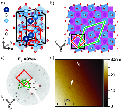
The orthorhombic unit cell of bulk crystalline CaTiO3 has lattice parameters of Å, Åand Å [29]. An approximate representation of the orthorhombic unit cell can be made by a pseudo-cubic unit cell as marked in Fig.1a). The lattice parameters of the pseudo-cubic unit cell Å are similar to cubic SrTiO3 with a lattice mismatch of approximately 2%.
In LEED we can identify the primary diffraction spots corresponding to the pseudo-cubic unit cell. Further we observe spots indicating a c(42) surface reconstruction of the pseudo-cubic lattice with domains rotated 90∘ with respect to each other (see Fig.1b) and c)). The (11) TiO2 terminated surface at the vacuum interface of TMO perovskites might be unstable due to the unshared oxygen atom of the TiO2 polyhedron sticking out of the surface. Of the surface reconstructions reported for the closely related SrTiO3 system, c(42) reconstruction has also been observed [30, 31, 32, 33].
The AFM topography in Fig.1d) shows that the films are of low roughness and follow the substrate steps with a terrace size of approximately 200 nm. However, the AFM measurements do not have the resolution required to observe the surface reconstruction. The observed presence of domain walls is a further indication of the existence of multiple rotated domains corroborating the LEED data.
3 Results and discussion
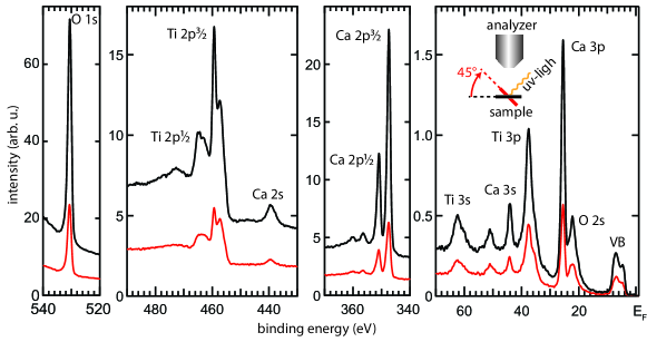
The XPS spectrum of the films in Fig.2, measured with a photon energy of = 600 eV, shows clear signatures of the expected calcium, titanium and oxygen core levels with no detectable contamination. Comparing the spectra taken with the sample surface normal to the analyzer to the more surface sensitive measurement taken at an angle of 45∘ between the sample normal and the analyzer axis (see sketch inset in Fig.2) we can confirm the TiO2 termination of the grown films. This termination of the film surface is expected due to the TiO2 termination of the SrTiO3 substrate [34]. When comparing the peak areas () after background subtraction the ratio of 0.75 at normal emission is significantly higher than the ratio of 0.65 measured at an emission angle of 45∘.

All the titanium peaks show a shoulder towards lower binding energy, indicating the existence of titanium atoms with different valency. The increase of the surface located Ti 3+ shoulder is a light induced effect commonly observed in this class of materials [16]. The appearance of Ti 3+ ions is likely linked to a distortion of the TiO2 octahedron, for example due to the creation of oxygen vacancies in the surface region and/or a structural rearrangement and buckling of the surface layers.

The Ti 2p as well as the Ca 2p core levels show plasmon loss peaks in their shake-up tail with an energy loss of 13.2 eV for titanium and 9 eV for calcium. Plasmon loss peaks with this loss energy of the Ti 2p core levels have been observed in other perovskites. The measured plasmon energy corresponds to surface plasmons present in TiO2 where the plasmons are trapped at the interface of the metallic surface and the dielectric bulk due to the sudden change in dielectric constant. [35, 36, 37, 38]
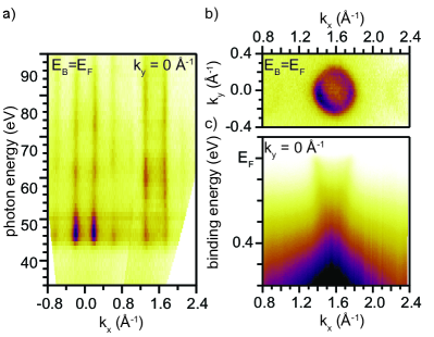
Consequently, we also expect metallic states to be present at the surface of our CaTiO3 films. Indeed, the ARPES measurements in Fig.3 show an electron-like surface state. The scan over a wide range of photon energies in Fig.3a) shows no dispersion of these states with out-of-plane momentum, verifying their two-dimensional nature. In contrast to the well-studied metallic states present at the surface of SrTiO3 (001) and KTaO3 (001) [12, 13, 14, 15, 16] we have no indication of three-dimensional features, making the 2DEG the only states contributing to the metallicity. Similar to the other perovskites the spectral intensity of the 2DEG at the CaTiO3 surface increases under UV-irradiation. This is attributed to light induced surface rearrangements and induced carriers [16].
The circular Fermi surface of is depicted in Fig.3b) and the corresponding clear free-electron-like parabolic band along the high symmetry direction in Fig.3c). The in-plane momentum Å-1 at the ring center, corresponding to the momentum of , is equal to a lattice parameter of Å. This is in good agreement with the lattice parameter of the pseudo-cubic unit cell of CaTiO3 and the SrTiO3 substrate. Also clearly visible in Fig.3a) is the intensity at the Fermi energy of an additional, folded parabola between and due to the surface reconstruction observed also in LEED as described in section 2. Similar band folding has been observed for the (14) reconstructed anatase TiO2 films [39].

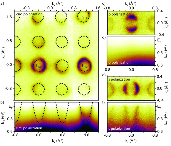
The band structure of the 2DEG in Fig.3c) and 4b) can be fitted with a free-electron-like parabola yielding an effective mass of , a Fermi momentum of Å-1, a Fermi velocity of m/s, and a band minimum at a binding energy of 400 meV. This corresponds to a charge carrier density per parabola of or with Å. This charge carrier density is similar to SrTiO3 [13, 16] while the band width is significantly higher and the effective mass much lower than for SrTiO3 and KTaO3. The ARPES measurements with s- and p-polarized light in Fig.4(c-f) confirm the -symmetry of the 2DEG with no indications of bands with - or -symmetry. The 2DEG thus consists of the Ti 3dxy bands splitted from dxz/dyz by crystal field splitting and partially filled due to surface band bending and light induced carriers.
With the absence of the Ti 3dxz and 3dyz bands and the two-dimensional Ti 3dxy bands at relatively high binding energies, the splitting between the dxy and dxz/dyz-bands has to be large, at least of the size of the observed bandwidth of 400 meV. This splitting is considerably larger than the 240 meV measured for SrTiO3 [16] but smaller than for TiO2 anatase where 1 eV is reported [18, 19]. For the orthorhombic oxide LaAlO3 a comparable noncubic crystal field splitting of 120 meV to 300 meV for the sub shell is reported [40]. However, there is no detectable additional splitting of the Ti 3dxy band as observed for SrTiO3 [17]. Comparing SrTiO3 to CaTiO3 the increased rotation of the TiO3 octahedron in the later due to the orthorhombicity will likely reduce the local electric fields as observed in other perovskites [41]. The resulting weak polarization field at the surface could be the reason that the splitting is too small to be observed in our data.
The results of the fitting are indicated in Fig.4a) and b) showing the circular Fermi surface composed by parabolic bands for the primary -points as well as for the reconstructed -points. Along the direction, the Fermi surfaces and parabolic bands corresponding to the folded -points, which are present as a result of the reconstruction, are clearly visible in the data. However their intensity is weaker than the signal of the 2DEG at the primary -points. In contrast to the folding along the high-symmetry direction, the -points offset by in direction are not present in the data. A possible reason for this is a change of the reconstruction from c(42) either to a combination of (21) and c(22) or more likely to p(22) under irradiation with UV-light. Since we observe an increasing intensity of the 2DEG as well as the described formation of a low binding energy shoulder on the titanium core levels under UV-light, a change of reconstruction under light due to the deposited energy is plausible.
4 Summary
In conclusion, we have revealed the existence of metallic states at the surface of CaTiO3 films consisting solely of a 2DEG. The 2DEG has a band width of 400 meV, indicating a large splitting between the unoccupied Ti 3dxz/dyz bands and the two-dimensional 3dxy bands. Due to its metallicity, the surface also hosts plasmons visible as loss peaks in the XPS data. The bands are folded according to the surface reconstruction that is likely changed from c(42) to p(2) under UV irradiation. Due to the lack of higher-dimensional conducting channels and the affinity of the system to adapt to its surface structure, various paths open up to directly manipulate the surface states. This manipulation may give direct access to the transport properties of the system and its coupling to overlayers. With the possibility to induce ferroelectricity into the quantum paraelectric materials CaTiO3 and SrTiO3 by mutual doping, the phase space is open to probe the effect of ferroelectricity on the 2DEG hosted by both of these materials.
Acknowledgments
We acknowledge financial support from the Swiss National Science foundation Project No. PP00P2_144742/1.
References
- [1]
- [2] A. Ohtomo, H. Hwang, A high-mobility electron gas at the LaAlO3/SrTiO3 heterointerface, Nature 427 (6973) (2004) 423–426.
-
[3]
Y. Hotta, T. Susaki, H. Y. Hwang,
Polar
discontinuity doping of the LaVO3/SrTiO3 interface, Phys. Rev. Lett.
99 (2007) 236805.
doi:10.1103/PhysRevLett.99.236805.
URL http://link.aps.org/doi/10.1103/PhysRevLett.99.236805 - [4] P. Perna, D. Maccariello, M. Radovic, U. Scotti di Uccio, I. Pallecchi, M. Codda, D. Marré, C. Cantoni, J. Gazquez, M. Varela, et al., Conducting interfaces between band insulating oxides: The LaGaO3/SrTiO3 heterostructure, Applied Physics Letters 97 (15) (2010) 152111.
-
[5]
E. Di Gennaro, U. S. di Uccio, C. Aruta, C. Cantoni, A. Gadaleta, A. R. Lupini,
D. Maccariello, D. Marré, I. Pallecchi, D. Paparo, P. Perna, M. Riaz, F. M.
Granozio, Persistent
photoconductivity in 2D electron gases at different oxide interfaces,
Advanced Optical Materials 1 (11) (2013) 834–843.
doi:10.1002/adom.201300150.
URL http://dx.doi.org/10.1002/adom.201300150 -
[6]
G. Chen, L. Balents,
Ferromagnetism
in itinerant two-dimensional systems, Phys. Rev. Lett. 110 (2013)
206401.
doi:10.1103/PhysRevLett.110.206401.
URL http://link.aps.org/doi/10.1103/PhysRevLett.110.206401 -
[7]
N. Reyren, S. Thiel, A. D. Caviglia, L. F. Kourkoutis, G. Hammerl, C. Richter,
C. W. Schneider, T. Kopp, A.-S. Rüetschi, D. Jaccard, M. Gabay, D. A.
Muller, J.-M. Triscone, J. Mannhart,
Superconducting
interfaces between insulating oxides, Science 317 (5842) (2007) 1196–1199.
arXiv:http://www.sciencemag.org/content/317/5842/1196.full.pdf,
doi:10.1126/science.1146006.
URL http://www.sciencemag.org/content/317/5842/1196.abstract - [8] K. Ueno, S. Nakamura, H. Shimotani, A. Ohtomo, N. Kimura, T. Nojima, H. Aoki, Y. Iwasa, M. Kawasaki, Electric-field-induced superconductivity in an insulator, Nature materials 7 (11) (2008) 855–858.
-
[9]
S. Thiel, G. Hammerl, A. Schmehl, C. W. Schneider, J. Mannhart,
Tunable
quasi-two-dimensional electron gases in oxide heterostructures, Science
313 (5795) (2006) 1942–1945.
arXiv:http://www.sciencemag.org/content/313/5795/1942.full.pdf,
doi:10.1126/science.1131091.
URL http://www.sciencemag.org/content/313/5795/1942.abstract - [10] C. Cen, S. Thiel, G. Hammerl, C. Schneider, K. Andersen, C. Hellberg, J. Mannhart, J. Levy, Nanoscale control of an interfacial metal–insulator transition at room temperature, Nature materials 7 (4) (2008) 298–302.
- [11] A. Brinkman, M. Huijben, M. Van Zalk, J. Huijben, U. Zeitler, J. Maan, W. Van der Wiel, G. Rijnders, D. Blank, H. Hilgenkamp, Magnetic effects at the interface between non-magnetic oxides, Nature materials 6 (7) (2007) 493–496.
- [12] A. F. Santander-Syro, O. Copie, T. Kondo, F. Fortuna, S. Pailhès, R. Weht, X. G. Qiu, F. Bertran, A. Nicolaou, A. Taleb-Ibrahimi, P. L. Fèvre, G. Herranz, M. Bibes, N. Reyren, Y. Apertet, P. Lecoeur, A. Barthélémy, M. J. Rozenberg, Two-dimensional electron gas with universal subbands at the surface of SrTiO3, Nature 469 (2011) 189. doi:http://dx.doi.org/10.1038/nature09720.
- [13] W. Meevasana, P. D. C. King, R. H. He, S.-K. Mo, M. Hashimoto, A. Tamai, P. Songsiriritthigul, F. Baumberger, Z.-X. Shen, Creation and control of a two-dimensional electron liquid at the bare SrTiO3 surface, Nat Mater 10 (2011) 114. doi:http://dx.doi.org/10.1038/nmat2943.
-
[14]
P. D. C. King, R. H. He, T. Eknapakul, P. Buaphet, S. K. Mo, Y. Kaneko,
S. Harashima, Y. Hikita, M. S. Bahramy, C. Bell, Z. Hussain, Y. Tokura, Z. X.
Shen, H. Y. Hwang, F. Baumberger, W. Meevasana,
Subband
structure of a two-dimensional electron gas formed at the polar surface of
the strong spin-orbit perovskite KTaO3, Physical Review Letters
108 (11) (2012) 117602–.
URL http://link.aps.org/doi/10.1103/PhysRevLett.108.117602 -
[15]
A. F. Santander-Syro, C. Bareille, F. Fortuna, O. Copie, M. Gabay, F. Bertran,
A. Taleb-Ibrahimi, P. Le Fèvre, G. Herranz, N. Reyren, M. Bibes,
A. Barthélémy, P. Lecoeur, J. Guevara, M. J. Rozenberg,
Orbital symmetry
reconstruction and strong mass renormalization in the two-dimensional
electron gas at the surface of KTaO3, Phys. Rev. B 86 (2012) 121107.
doi:10.1103/PhysRevB.86.121107.
URL http://link.aps.org/doi/10.1103/PhysRevB.86.121107 -
[16]
N. C. Plumb, M. Salluzzo, E. Razzoli, M. Månsson, M. Falub, J. Krempasky,
C. E. Matt, J. Chang, M. Schulte, J. Braun, H. Ebert, J. Minár, B. Delley,
K.-J. Zhou, T. Schmitt, M. Shi, J. Mesot, L. Patthey,
M. Radović,
Mixed
dimensionality of confined conducting electrons in the surface region of
SrTiO3, Phys. Rev. Lett. 113 (2014) 086801.
doi:10.1103/PhysRevLett.113.086801.
URL http://link.aps.org/doi/10.1103/PhysRevLett.113.086801 - [17] A. Santander-Syro, F. Fortuna, C. Bareille, T. Rödel, G. Landolt, N. Plumb, J. Dil, M. Radović, Giant spin splitting of the two-dimensional electron gas at the surface of SrTiO3, Nature materials 13 (12) (2014) 1085–1090.
-
[18]
S. Moser, L. Moreschini, J. Jaćimović, O. S. Barišić, H. Berger,
A. Magrez, Y. J. Chang, K. S. Kim, A. Bostwick, E. Rotenberg, L. Forró,
M. Grioni,
Tunable
polaronic conduction in anatase TiO2, Phys. Rev. Lett. 110 (2013)
196403.
doi:10.1103/PhysRevLett.110.196403.
URL http://link.aps.org/doi/10.1103/PhysRevLett.110.196403 - [19] Z. Wang, S. M. Walker, A. Tamai, Y. Wang, Z. Ristic, F. Y. Bruno, A. De La Torre, S. Riccò, N. Plumb, M. Shi, et al., Tailoring the nature and strength of electron-phonon interactions in the SrTiO3 (001) 2D electron liquid, Nature materials 15 (8) (2016) 835–839.
- [20] J. Lee, F. Schmitt, R. Moore, S. Johnston, Y.-T. Cui, W. Li, M. Yi, Z. Liu, M. Hashimoto, Y. Zhang, et al., Interfacial mode coupling as the origin of the enhancement of Tc in FeSe films on SrTiO3, Nature 515 (7526) (2014) 245–248.
-
[21]
S. N. Rebec, T. Jia, C. Zhang, M. Hashimoto, D.-H. Lu, R. G. Moore, Z.-X. Shen,
Coexistence of
replica bands and superconductivity in FeSe monolayer films, Phys. Rev.
Lett. 118 (2017) 067002.
doi:10.1103/PhysRevLett.118.067002.
URL http://link.aps.org/doi/10.1103/PhysRevLett.118.067002 -
[22]
V. Lemanov, A. Sotnikov, E. Smirnova, M. Weihnacht, R. Kunze,
Perovskite
CaTiO3 as an incipient ferroelectric, Solid State Communications
110 (11) (1999) 611 – 614.
doi:http://dx.doi.org/10.1016/S0038-1098(99)00153-2.
URL http://www.sciencedirect.com/science/article/pii/S0038109899001532 - [23] J. Bednorz, K. Müller, Sr1-xCaxTiO3: An xy quantum ferroelectric with transition to randomness, Physical Review Letters 52 (25) (1984) 2289.
- [24] R. Ranjan, D. Pandey, Antiferroelectric phase transition in (Sr1-xCax) TiO3: II. x-ray diffraction studies, Journal of Physics: Condensed Matter 13 (19) (2001) 4251.
- [25] M. Yamamoto, H. Ohta, K. Koumoto, Thermoelectric phase diagram in a CaTiO3–SrTiO3–BaTiO3 system, Applied physics letters 90 (7) (2007) 072101.
- [26] M. Yashima, R. Ali, Structural phase transition and octahedral tilting in the calcium titanate perovskite CaTiO3, Solid State Ionics 180 (2) (2009) 120–126.
- [27] Q. Fan, J. Yang, C. Deng, J. Zhang, J. Cao, Electronic structure and optical properties of CaTiO3: An ab initio study, in: Sixth International Conference on Electronics and Information Engineering, International Society for Optics and Photonics, 2015, pp. 97942I–97942I.
- [28] S. Tariq, A. Ahmed, S. Saad, S. Tariq, Structural, electronic and elastic properties of the cubic CaTiO3 under pressure: A DFT study, AIP Advances 5 (7) (2015) 077111.
-
[29]
H. F. Kay, P. C. Bailey,
Structure and properties of
CaTiO3, Acta Crystallographica 10 (3) (1957) 219–226.
doi:10.1107/S0365110X57000675.
URL https://doi.org/10.1107/S0365110X57000675 - [30] M. R. Castell, Scanning tunneling microscopy of reconstructions on the SrTiO3 (001) surface, Surface Science 505 (2002) 1–13.
-
[31]
N. Erdman, O. Warschkow, M. Asta, K. R. Poeppelmeier, D. E. Ellis, L. D. Marks,
Surface structures of SrTiO3
(001): a TiO2-rich reconstruction with a c(4 2) unit cell,
Journal of the American Chemical Society 125 (33) (2003) 10050–10056, pMID:
12914468.
arXiv:http://dx.doi.org/10.1021/ja034933h, doi:10.1021/ja034933h.
URL http://dx.doi.org/10.1021/ja034933h - [32] K. Iwaya, T. Ohsawa, R. Shimizu, T. Hashizume, T. Hitosugi, Atomically resolved surface structure of SrTiO3 (001) thin films grown in step-flow mode by pulsed laser deposition, Applied physics express 3 (7) (2010) 075701.
- [33] G.-z. Zhu, G. Radtke, G. A. Botton, Bonding and structure of a reconstructed (001) surface of SrTiO3 from TEM, Nature 490 (7420) (2012) 384–387.
- [34] M. Radovic, N. Lampis, F. Miletto Granozio, P. Perna, Z. Ristic, M. Salluzzo, C. Schlepütz, U. Scotti di Uccio, Growth and characterization of stable SrO-terminated SrTiO3 surfaces, Applied Physics Letters 94 (2009) 022901.
-
[35]
S. Sen, J. Riga, J. Verbist,
2s
and 2p x-ray photoelectron spectra of Ti4+ ion in TiO2, Chemical
Physics Letters 39 (3) (1976) 560 – 564.
doi:http://dx.doi.org/10.1016/0009-2614(76)80329-6.
URL http://www.sciencedirect.com/science/article/pii/0009261476803296 -
[36]
D. K. G. de Boer, C. Haas, G. A. Sawatzky,
Exciton satellites in
photoelectron spectra, Phys. Rev. B 29 (1984) 4401–4419.
doi:10.1103/PhysRevB.29.4401.
URL http://link.aps.org/doi/10.1103/PhysRevB.29.4401 -
[37]
A. E. Bocquet, T. Mizokawa, K. Morikawa, A. Fujimori, S. R. Barman, K. Maiti,
D. D. Sarma, Y. Tokura, M. Onoda,
Electronic structure
of early 3d-transition-metal oxides by analysis of the 2p core-level
photoemission spectra, Phys. Rev. B 53 (1996) 1161–1170.
doi:10.1103/PhysRevB.53.1161.
URL http://link.aps.org/doi/10.1103/PhysRevB.53.1161 - [38] A. Bahadur, S. K. Srivastava, Extrinsic and intrinsic plasmon effects in 2p1/2 x-ray photoemission satellites of scandium and titanium compounds, Trakia Journal of Sciences 8 (3) (2010) 29–34.
-
[39]
Z. Wang, Z. Zhong, S. McKeown Walker, Z. Ristic, J.-Z. Ma, F. Y. Bruno,
S. Riccò, G. Sangiovanni, G. Eres, N. C. Plumb, L. Patthey, M. Shi,
J. Mesot, F. Baumberger, M. Radovic,
Atomically precise
lateral modulation of a two-dimensional electron liquid in anatase TiO2
thin films, Nano Letters 17 (4) (2017) 2561–2567.
doi:10.1021/acs.nanolett.7b00317.
URL http://dx.doi.org/10.1021/acs.nanolett.7b00317 -
[40]
M. W. Haverkort, Z. Hu, A. Tanaka, G. Ghiringhelli, H. Roth, M. Cwik,
T. Lorenz, C. Schüßler-Langeheine, S. V. Streltsov, A. S. Mylnikova,
V. I. Anisimov, C. de Nadai, N. B. Brookes, H. H. Hsieh, H.-J. Lin, C. T.
Chen, T. Mizokawa, Y. Taguchi, Y. Tokura, D. I. Khomskii, L. H. Tjeng,
Determination
of the orbital moment and crystal-field splitting in LaTiO3, Phys. Rev.
Lett. 94 (2005) 056401.
doi:10.1103/PhysRevLett.94.056401.
URL https://link.aps.org/doi/10.1103/PhysRevLett.94.056401 -
[41]
D. Sando, A. Barthélémy, M. Bibes,
BiFeO3 epitaxial
thin films and devices: past, present and future, Journal of Physics:
Condensed Matter 26 (47) (2014) 473201.
URL http://iopscience.iop.org/0953-8984/26/47/473201