Tuning the topological states in metal-organic bilayers
Abstract
We have investigated the energetic stability and the electronic properties of metal-organic topological insulators bilayers (BLs), (MC4S4)3-BL, with M=Ni and Pt, using first-principles calculations and tight-binding model. Our findings show that (MC4S4)3-BL is an appealing platform to perform electronic band structure engineering, based on the topologically protected chiral edge states. The energetic stability of the BLs is ruled by van der Waals interactions; being the AA stacking the energetically most stable one. The electronic band structure is characterized by a combination of bonding and anti-bonding kagome band sets (KBSs), revealing that (NiC4S-BL presents a Z2-metallic phase, whereas (PtC4S-BL may present both Z2-metallic phase or quantum spin Hall phase. Those non-trivial topological states were confirmed by the formation of chiral edge states in (MC4S4)3-BL nanoribbons. We show that the localization of the edge states can be controlled with a normal external electric field, breaking the mirror symmetry. Hence, the sign of electric field selects in which layer each set of edge states are located. Such a control on the (layer) localization, of the topological edge states, bring us an additional and interesting degree of freedom to control the transport properties in layered metal-organic topological insulator.
I Introduction
Two dimensional (2D) topological insulators, based on organic hosts, have been the subject of numerous studies addressing not only fundamental issues, but also future technological applications. In a seminal work, Wang et al. Wang et al. (2013a) predicted a non-trivial topological phase in an organic lattice composed by a monolayer (ML) of three benzene molecules bonded to metal atoms, Pb and Bi. Soon after the successful synthesis of 2D metal-organic ML lattices of nickel bis(dithiolene), (NiC4S Kambe et al. (2013), theoretical studies based on first-principles calculations and single orbital tight-binding (TB) model, predicted a non-trivial topological phase in (NiC4S, characterized by the topological invariant Z2 [=1 in (NiC4S], and the formation of spin-polarized chiral edge states at the time-reversal-invariant momenta (TRIM) Wang et al. (2013b).
By exploiting the large variety of (possible) combinations of metal-organic hosts, other metal-organic frameworks (MOFs), with non-trivial topological phase, have been proposed in the past few years. For instance, keeping the kagome lattice of (NiC4S, but substituting Ni with Mn atoms, Zhao et al. Zhao et al. (2013) verified the quantum anomalous Hall (QAH) state in (MnC4S4)3. Here, the appearance of a ferromagnetic phase, mediated by the unpaired Mn-3 electrons, breaks the time-reversal symmetry of the original (NiC4S system. Further QAH state has also been predicted in 2D lattices of (i) trans-Au-THTAP, where the ferromagnetism arise due to a half-filled flat band Yamada et al. (2016) ; and (ii) triphenil-manganese (MnC4H5)3 Wang et al. (2013c), where ferromagnetically coupled Mn atoms are connected by benzene rings forming a honeycomb lattice. By keeping the same honeycomb structure of the benzene host, and substituting Mn with Pb atoms (triphenil-manganesetriphenil-lead), it has been predicted a non-magnetic ground state, where the spin-orbit coupling (SOC) promotes the QSH phase in (PbC4H5)3 Wang et al. (2013a). Further investigations Kim et al. (2016) pointed out that, mediated by an external electric field, the (PbC4H5)3 lattice presents an energetically stable ferrimagnetic QAH phase. Meanwhile, the recently synthesized Ni3(C18H12N6)2 MOF Sheberla et al. (2014) can be considered as the experimental realization of the so called topological Z2-metallic phase Pan et al. (2014) in MOFs. It is characterized by a kagome lattice, with a global energy gap at the edge of the Brillouin zone (K point), whereas the energy dispersion of the flat (kagome band) along the –K direction gives rise to a local gap at the point Zhao et al. (2014).
The design of 2D systems based on the MOFs is not limited by the metalorganic-host combinations. Based on the recent concept of van der Waals (vdW) heterostructures Geim and Grigorieva (2013), we may access a set of new/interesting electronic properties by stacking 2D MOFs, as we have testified in inorganic layered materials Radisavljevic et al. (2011). Currently we are facing a suitable synergy between the experimental works addressing the successful synthesis of stacked 2D MOFs Kitagawa et al. (2004); Colson and Dichtel (2013); Zhang et al. (2014); Sheberla et al. (2014); Rodriguez-San-Miguel et al. (2016); Sakamoto et al. (2016), and theoretical studies aiming the understanding of their physical properties; and propose the design of new atomic structures Adjizian et al. (2014); Zhou (2014) focusing on a set of desired electronic properties. For instance, the control of the topological states in stacked MOFs.
In this paper we investigate the energetic stability and the electronic properties of (MC4S4)3 (M=Ni and Pt) bilayers, (MC4S4)3-BLs. The present study was carried out through a combination of first-principles calculations and TB model. The energetic stability of the (MC4S4)3-BLs is ruled by vdW interactions; where (i) the electronic band structure of the most likely BL configuration (AA stacking) is characterized by a combination of bonding and anti-bonding kagome band sets (KBSs). The non-trivial nature of the energy gaps, induced by the SOC, was verified through the calculation of the edge states in (MC4S4)3-BL nanoribbons (NRs). (ii) Turning on an external electric field normal to the BL, we find that the electronic contributions from each ML are no longer symmetric; giving rise to an interlayer separation between the bonding and anti-bonding KBSs. By mapping the localization of the edge states, we find that they follow the same spacial separation pattern, showing that the (layer) localization of the topologically protected edge states in (MC4S4)3-BL NRs can be tuned by the external electric field. Based upon the first-principles calculations and a phenomenological model, we can infer that (i) and (ii), described above, will also take place in other vdW metal-organic BLs charaterized by a superposition of kagome bands.
II Method
The calculations were performed based on the DFT approach, as implemented in the VASP codeKresse and Furthmller (1996). The exchange correlation term was described using the GGA functional proposed by Perdew, Burke and Ernzerhof (PBE)Perdew et al. (1996). The Kohn-Sham orbitals are expanded in a plane wave basis set with an energy cutoff of 400 eV. The 2D Brillouin Zone (BZ) is sampled according to the Monkhorst-Pack methodMonkhorst and Pack (1976), using a gamma-centered 441 mesh for atomic structure relaxation and 661 mesh to obtain the self-consistent total charge density. The electron-ion interactions are taken into account using the Projector Augmented Wave (PAW) method Blöchl (1994). All geometries have been relaxed until atomic forces were lower than eV/Å. The metal-organic framework monolayer system is simulated considering a vacuum region in the direction perpendicular to the layers of at least Å. For MOF bilayers the van der Waals interaction (vdW-DF2Lee et al. (2010)) was considered to correctly describe the system. In this bilayer system the vacuum region is increased to at least Å to avoid periodic images interaction.
The real-space tight-binding (TB) Hamiltonian of kagome-hexagonal lattice Tang et al. (2011); Wang et al. (2013c) in the presence of intrinsic spin-orbit coupling can be written as
| (1) |
where each term is given by
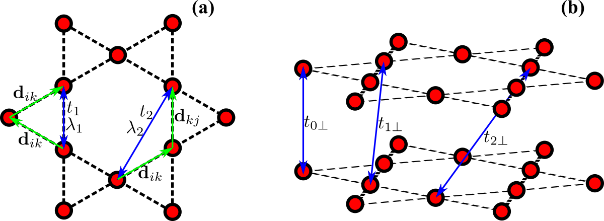
Here, and are the creation and annihilation operators for an electron with spin on site ; are the spin Pauli matrices. As depicted in Figs. 1(d) and (e), and are the vectors connecting the -th and -th sites to the -th nearest-neighbor in common; and are the strength of hopping and spin-orbit terms. The and refer to sums over nearest-neighbor and next-nearest-neighbor, respectively. See Sec. I of Supplemental Material (SM) sup for more details.
III Results and Discussions
III.1 Monolayer
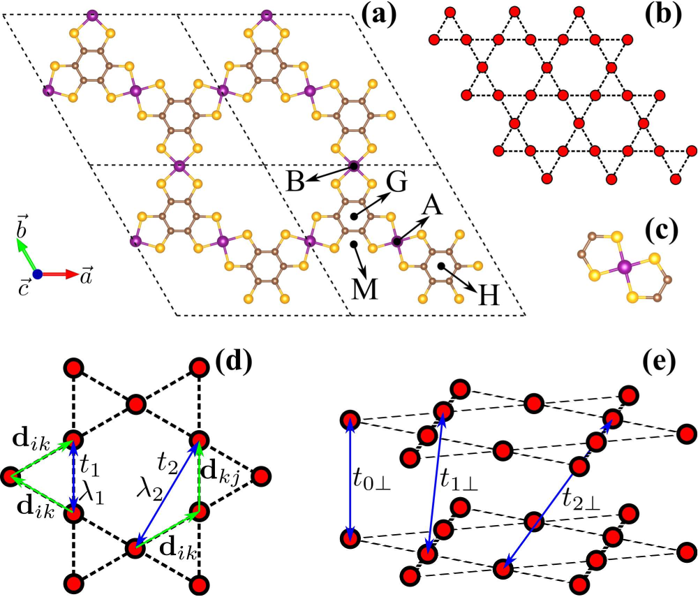
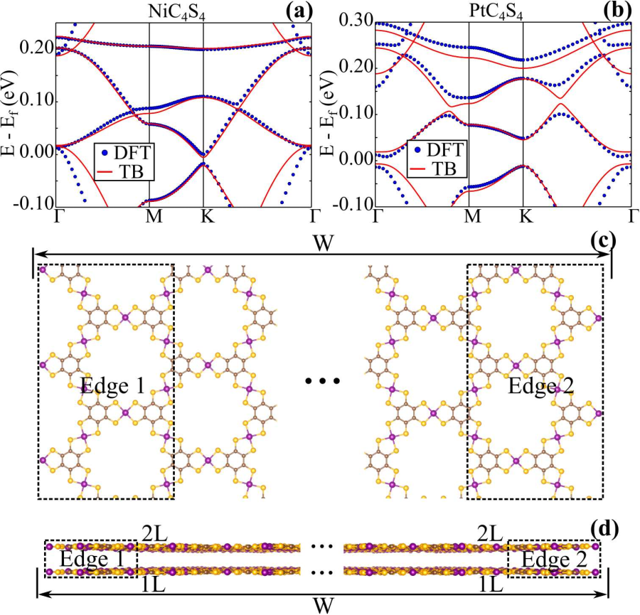
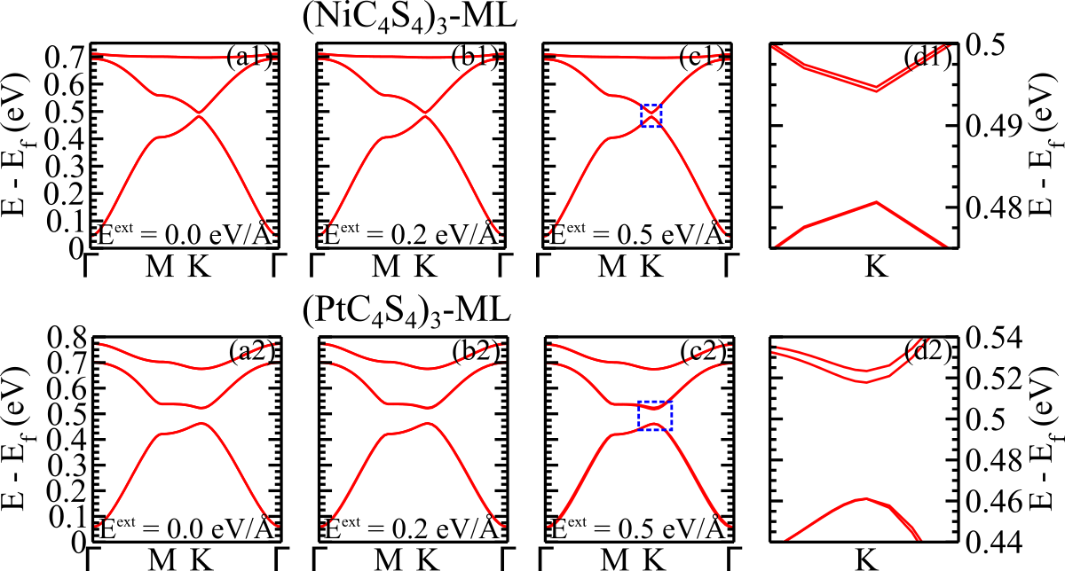
The metal organic framework of (MC4S4)3 monolayer, (MC4S4)3-ML, M = Ni and Pt, presents a hexagonal atomic structure [Fig. 1(a)], which can be viewed as a kagome lattice [Fig. 1(b)], where each site is occupied by a (MC4S4) molecule [Fig. 1(c)]. At the equilibrium geometry, we found that (NiC4S presents a lattice parameter () of 14.70 Å, which is in good agreement with recent experimental measurements Kambe et al. (2013), and first-principles DFT results Wang et al. (2013b). For (PtC4S we obtained Å, as the Pt covalent radius is greater than Ni, which is also in agreement with recent first-principles results Lü et al. (2017). The electronic band structures of both MOFs exhibit the typical kagome energy bands above the Fermi level (), within eV. These are graphene-like energy bands, with a Dirac cone at the K point, degenerated with a nearly flat band at the point, as shown in Figs. 2(a1) and (b1). Such degeneracies are removed by the SOC. In (NiC4S-ML we find non-trivial global energy gaps of 4 meV (indirect) and 14 meV (direct at the K point), and a local gap of 17 meV, between and at the point, Fig. 2(a2). Those (SOC induced) energy gaps are larger in (PtC4S-ML, i.e. 72 meV at and 60 meV at K, as shown in Fig. 2(b2). Due to the energy dispersion of , the former is not a global gap. The larger energy dispersion of can be attributed the next-nearest-neighbor interactions among the Pt atoms Zhou et al. (2014). The electronic band structures projected to the atomic orbitals, Figs. 2(a3) and (b3), reveal that the kagome band set of both (MC4S4)3 systems are formed by the hybridization of C and S orbitals of the organic host, with the metal and orbitals. As will be discussed below, such a hybridization picture is quite relevant for the electronic properties of the bilayer systems.
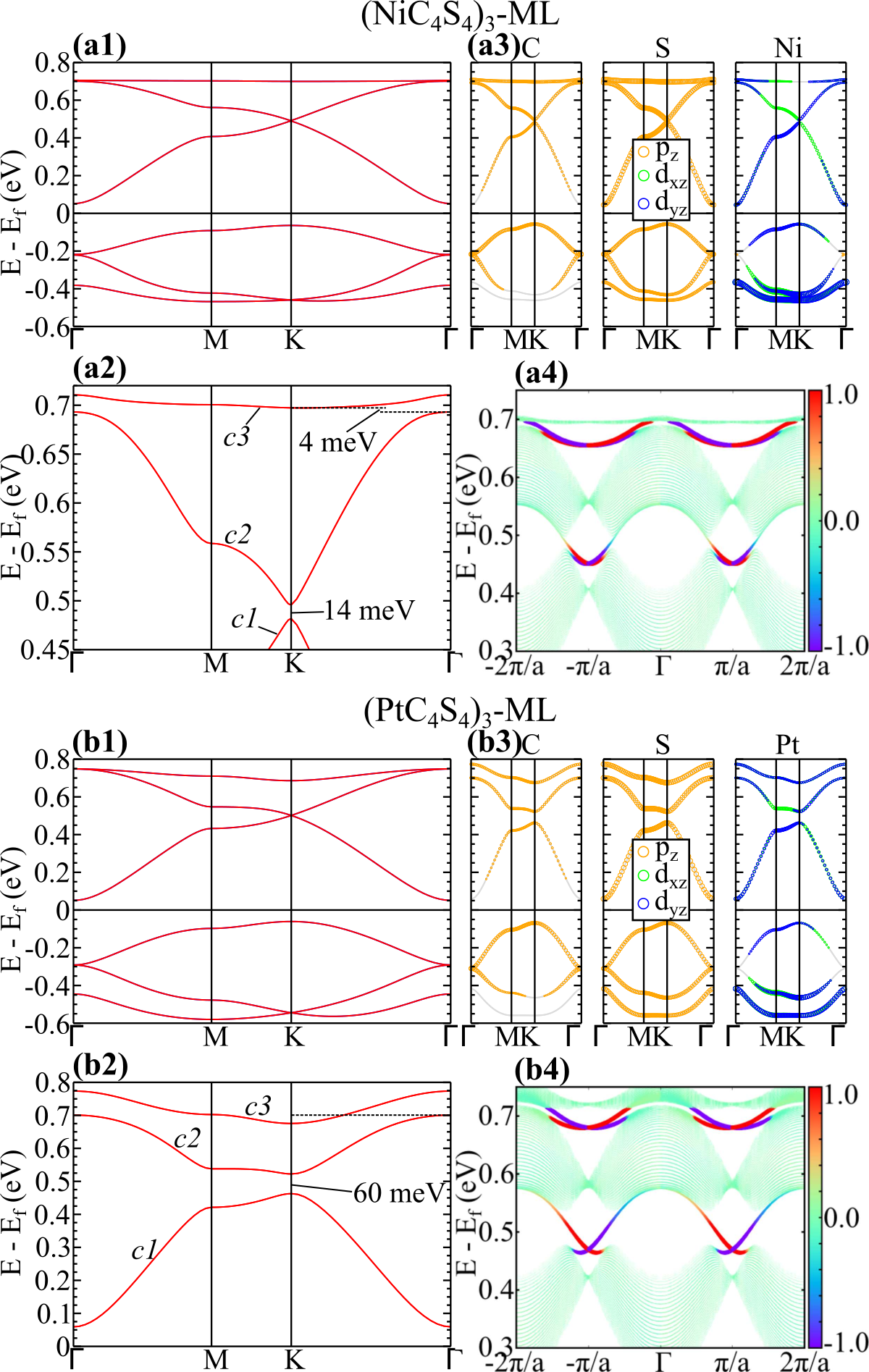
The energy gaps induced by the SOC between and at K, and between and at [Figs. 2(a2) and (b2)] characterize the QSH phase of (NiC4S, and (PtC4S. The topological phase of (NiC4S is well known Wang et al. (2013b). Here, based on the evolution of the Wannier Charge Centers (WCC), we found Z for both MOFs (Details in the SM sup ). However, due to the energy dispersion of in (PtC4S, the energy gap - at the point is a local gap, giving rise to the so called Z2-metallic state Zhao et al. (2014). Further verification of the QSH phase can be done by mapping the edge states of (NiC4S- and (PtC4S-ML. Based on the TB approach, we calculated the energy bands of (NiC4S- and (PtC4S-ML NRs. As depicted in Figs. 2(a4) and (b4), the formation of chiral spin-polarized edge states, degenerated at the TRIM, confirms the non-trivial topological phases of the (NiC4S and (PtC4S MLs. We have examined the formation of edge states for other edge geometries as detailed in sup .
III.2 Bilayer
In this section, based on first-principles calculations, firstly we investigate the energetic stability, and the electronic properties of the (MC4S4)3 BL systems; and next by combining first-principles calculations and the phenomenological model described below, we provide a comprehensive understanding of the interlayer-electronic tuning processes mediated by an external electric field and interlayer separation.
The energetic stability of (MC4S4)3-BL was examined by considering a set of different (MC4S4)3/(MC4S4)3 interface geometries, aligning sites X and Y [for X, Y A, B, G, H, and M, as indicated in Fig. 1(a)], i.e. the X site of one layer above the Y site of the other. In Table 1 we show the averaged interlayer equilibrium distance (), the root-mean-square deviation () of the atomic position perpendicularly to the (MC4S4)3 sheet, and the BL binding energy (). Here, we define as, , where is the total energy of an isolated monolayer, and is the total energy of the (MC4S4)3-BL for a given staking configuration. We found that the AA staking is the most stable one, with of 9.99 and 8.46 meV/Å2 (69 and 62 meV/atom) for (NiC4S-BL and (PtC4S-BL, respectively. Followed by the AG stacking by 0.70 and 0.36 meV/Å2 (4.8 and 2.6 meV/atom). The energetic stability of those (MC4S4)3-BLs is ruled by vdW interactions. It is worth noting that the binding strength of the (MC4S4)3-BL is larger compared with other energetically stable 2D-vdW systems like graphene Lebedeva et al. (2011); Mostaani et al. (2015) and boron-nitride Marom et al. (2010); Gao and Tkatchenko (2015) bilayers. There are no chemical bonds at the (MS4C4)3/(MS4C4)3 interface region, where we found of 3.64 and 3.66 Å for (NiC4S and (PtC4S BLs, and Å, thus indicating that the corrugations of the (MC4S4)3 sheets are negligible in the AA stacking. In contrast, the other stacking geometries present between 0.1 and 0.2 Å.
| (NiC4S | (PtC4S | |||||
|---|---|---|---|---|---|---|
| Staking Geometry | ||||||
| AA | 9.99 | 3.64 | 0.01 | 8.46 | 3.66 | 0.01 |
| AB | 8.51 | 3.37 | 0.22 | 6.92 | 3.37 | 0.23 |
| AM | 9.26 | 3.64 | 0.08 | 7.97 | 3.60 | 0.15 |
| AG | 9.29 | 3.57 | 0.12 | 8.10 | 3.51 | 0.18 |
| GH | 8.56 | 3.35 | 0.11 | 6.92 | 3.37 | 0.13 |
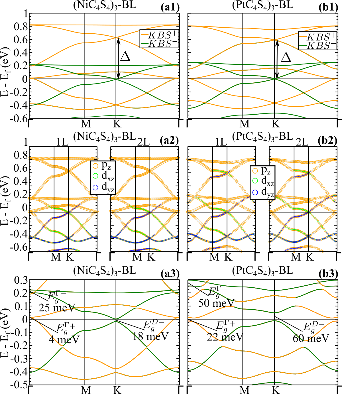
Next we discuss the electronic properties of the energetically most stable (NiC4S and (PtC4S BLs. Initially, we will examine the electronic band structure without the SOC. The electronic structure of the BLs can be described as a combination of anti-bonding (KBS+) and bonding (KBS-) kagome band sets, indicated by orange and green solid lines in Figs. 3(a1) and (b1). The Dirac bands of each KBSs are preserved, where the KBS+ and KBS- are separated (in energy) by ; giving rise to one Dirac point at about eV and another lying on the Fermi level. Here, provide a measure of the interlayer coupling between the (MC4S4)3 MLs sup . Further projected energy bands [Figs. 3(a2) and (b2)] show that (i) each layer exhibits the same electronic contribution on the KBS+ and KBS-, where (ii) the energy bands are composed by and orbitals of the transition metals (Ni and Pt) hybridized with C and S orbitals of the organic host.
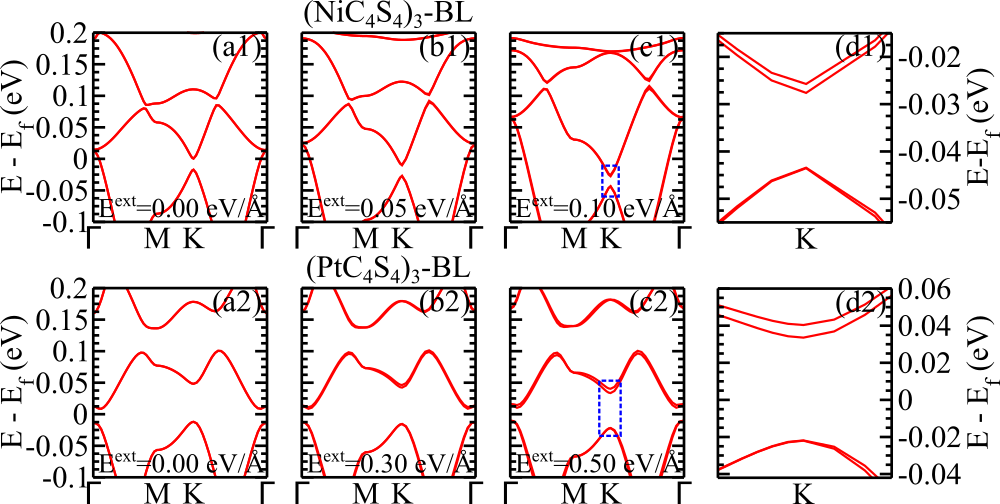
The SOC yields energy gaps at the Dirac points (). For instance, in (NiC4S-BL [Fig. 3(a3)] we find a energy gap of 18 meV in KBS- (). This is a local energy gap, due to the presence of partially occupied metallic bands near the point. The SOC also induces energy gaps at the point. As shown in Fig. 3(a3), we find a small local gap of 4 meV in the KBS+ () near the Fermi level, and another local gap of 25 meV at eV in the KBS- (). In contrast, (PtC4S BL presents a global gap of 22 meV at the Fermi level (), followed by of 60 meV, and a local gap of 50 meV at the point () [Fig.3(b3)]. As will be discussed below, those energy gaps induced by the SOC will dictate the formation of topologically protected edge states in the (MC4S4)3-BLs.
To model the DFT results presented above, we propose a phenomenological Hamiltonian to describe the interaction between layers. Assuming the mirror symmetry of the AA stacking, the Hamiltonian reads
| (2) |
where, , represents the Hamiltonian of each monolayer separately, diagonal on the base ( bands, layers), which gives the kagome band dispersions; () are the Pauli matrix in the layer space, and the coupling term between the layers. In this model, each layer will interact forming the highest energy (anti-bonding, ) and the lowest energy (bonding, ) KBSs, energetically separated by . In this case, the Dirac bands at the Fermi level are given by the bonding KBSs, green solid lines in Fig. 3(a1) and (b1). The mirror symmetry imposes that , for # = 1, 2.
The mirror symmetry can be suppressed upon the interaction of the (MC4S4)3-BLs with a solid surface, or due to the presence of an external electric field perpendicular to the (MC4S4)3 layer. The latter can be expressed by adding a potential difference between the layers in ,
| (3) |
Here, the potential difference due to only the external electric field () will be , but the charge rearrangement at the (MC4S4)3/(MC4S4)3 interface can reduce this potential difference such that, . Further discussion on the proposed model can be found in the Supplemental Material sup , Sec. II. Therefore, in this model the contribution of each layer to an given state is dependent.
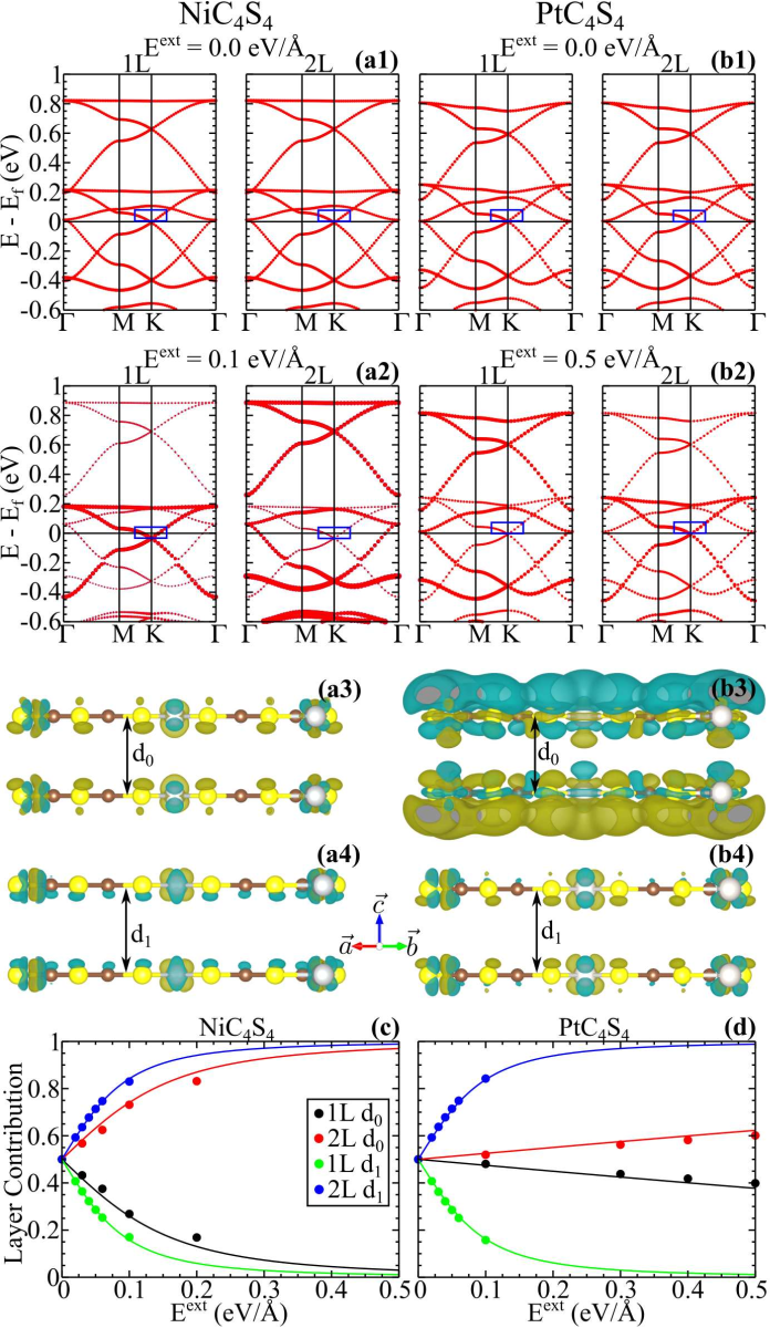
Initially, the effect of external electric field was studied based on the first-principles approach. In Figs. 4(a1) and (b1) we present the electronic band structures of the (PtC4S and (NiC4S BLs for . The mirror symmetry is fulfilled and both layer contributes equally for each state. The size of red circles is proportional to the layer contribution to each state, . By turning on the external electric field (), there is an unbalance on the charge density distribution between the MLs, Figs. 4(a2) and (b2); followed by an increase on the energy separation between the kagome bands, eV as the electric field module increase from eV/Å in (NiC4S-BL. In contrast, such an increase of , as a function of the external field, is almost negligible in (PtC4S-BL. For the electric field module increasing from eV/Å, the separation between the kagome bands changes by less than 0.03 eV ( eV).
The dependence of with the external electric field can be understood by analyzing the changes on the total charge density () as a function of and the interlayer distance . For a given value of , we can define as,
| (4) |
where and represent the total charge densities of the (MC4S4)3 BL at and , respectively. Our results of for the (NiC4S and (PtC4S BLs show that, (i) at the equilibrium geometry ( Å), there is no charge transfer between the (NiC4S MLs [Fig. 4(a3)]; in contrast (ii) a net charge transfer takes place between the (PtC4S MLs [Fig. 4(b3)]. Such a net charge transfer gives rise to an intrinsic local electric field which can be written as, ; reducing the potential difference between the (PtC4S MLs, in agreement with the small changes on the energy separation between the kagome bands, . By increasing the interlayer distance, for instance Å, we found that (i) the electronic interaction between the (MC4S4)3 MLs reduces, as well as the coupling term . We found eV (first-principles calculations) for both (MC4S4)3 BLs; and (ii) there is a reduction on the net charge transfer between the MLs due to the external electric field, as depicted in Figs. 4(a4) and (b4) for (NiC4S and (PtC4S, respectively.
As shown in Figs. 4(a2) and (b2), the layer contribution on the KBSs can be controlled by an external electric field. Here we will consider the electronic states around the Dirac point near the the Fermi level, indicated by (blue) rectangles in Figs. 4(a1)-(a2) and 4(b1)-(b2). The calculated partial charge densities within those rectangles, and , are shown in Figs. 4(c) and (d) for from 0 to 0.5 eV/Å. Our first-principles results are indicated by colored circles, and solid lines indicate the ones obtained by using the phenomenological model. At we have , i. e. both layers present the same electronic contribution as the mirror symmetry is fulfilled. For lower values of , , the electronic contribution of each layer exhibits a linear behaviour, where the tangent modulus is sup . The separation of the partial charge densities between the MLs is strengthened for larger interlayer distances. For instance, at the equilibrium geometry, Å, we find and , which corresponds to a charge density separation ratio (),
of 0.37 for eV/Å in (NiC4S-BL; increasing to 3.9 Å, the charge density separation increases, for the same value of . On the other hand, the net charge transfers between the (PtC4S MLs result in for a greater range of , giving rise to a linear response of the layer contribution, even for eV/Å, black and red lines in Fig. 4(d). Indeed, for Å the charge density separation is very small, we find and , for eV/Å. On the other hand, increasing the interlayer distance to Å, the charge transfer is suppressed [Fig. 4(b4)], and we find for eV/Å, which is practically the result obtained in (NiC4S-BL.
It is worth noting that (i) by inverting the direction, the layer localization also inverts (), and (ii) in the present scenario the charge density separation in (MC4S4)3 BLs is ruled by the suppression of the mirror symmetry. Here we have considered the suppression of the mirror symmetry through an external electric field, but the same behavior is expected in other cases, e.g. the presence of a substrate. In the next section we discuss the bilayers ribbons and the location of the topologically protected edge states, by the breaking of the mirror symmetry.
III.3 Bilayer Nanoribbon
In this section we will discuss the edge states of BL nanoribbons, in order to provide a more complete picture of the electronic properties of the (MC4S4)3-BLs. Here, the electronic band structure of (NiC4S- and (PtC4S-BLs, obtained through first-principles calculations, was fitted within the TB approach considering the intralayer and interlayer hoppings, and two orbitals (A and B) per site of the kagome bilayer-lattice (details in Sec. I of the SM). As shown in Figs. 5(a) and (b), the energy dispersions obtained through the TB Hamiltonian (red lines) present a reasonably well correspondence with the ones obtained by the first-principles calculations approach (blue circles), where the main features of the band structure are well described.
Similarly to the monolayers, the bilayers also have a topological invariant. However, here it shows a for each set of orthogonal subspaces. For the mirror symmetry case, these are the bonding (KBS+) and anti-bonding (KBS-) states. For a finite it is still possible to define two orthogonal sets [see Supplemental Material sup ], which are similar to the KBS± states. Consequently, in the following we find two sets of edge states, one for each orthogonal subspace.
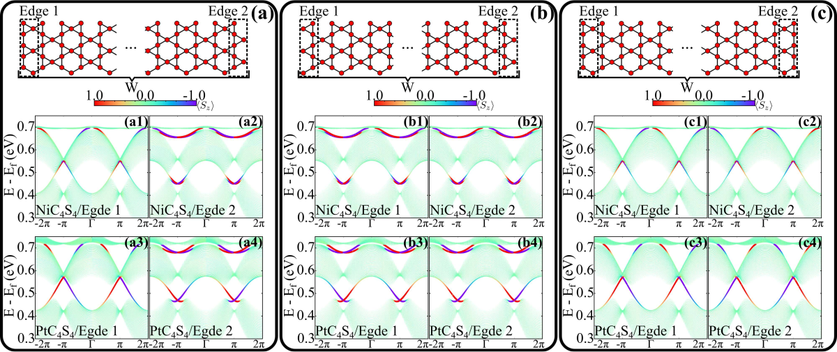
In order to identify these topologically protected edge states we have considered nanoribbon widths (W) of and nm for (NiC4S and (PtC4S BLs, Figs. 5(c) and (d).
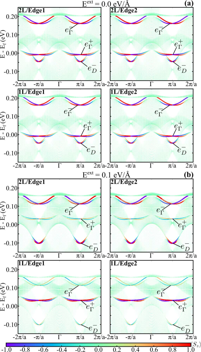
In Figs. 6 and 7 we present the spin-polarized energy bands projected on the edge atoms indicated in Figs. 5(c) and (d). The formation of chiral edge states, degenerated at the TRIM, confirms the topological phases of the (NiC4S and (PtC4S BLs. Figures 6(a) and 7(a) show three sets of metallic edge states near the Fermi level, viz.: , , and , degenerated at the TRIM k = /a and /a. Those metallic bands come from the (non-trivial) energy gaps induced by the SOC, between (i) the kagome bands at the point, , and , and (ii) the Dirac states at the K point, . In (NiC4S-BL, the energy gaps (i) and (ii) [Fig. 3(a3)] are not global, however, the formation of spin polarized chiral edge states supports the so called Z2-metallic phase. In contrast, (PtC4S-BL presents a (large) global energy gap of 22 meV () at the Fermi level, Fig. 3(b3). Thus, in order to acess the QSH phase in (PtC4S-BL, it is not necessary any external doping to place the Fermi level in the non trivial energy gap.
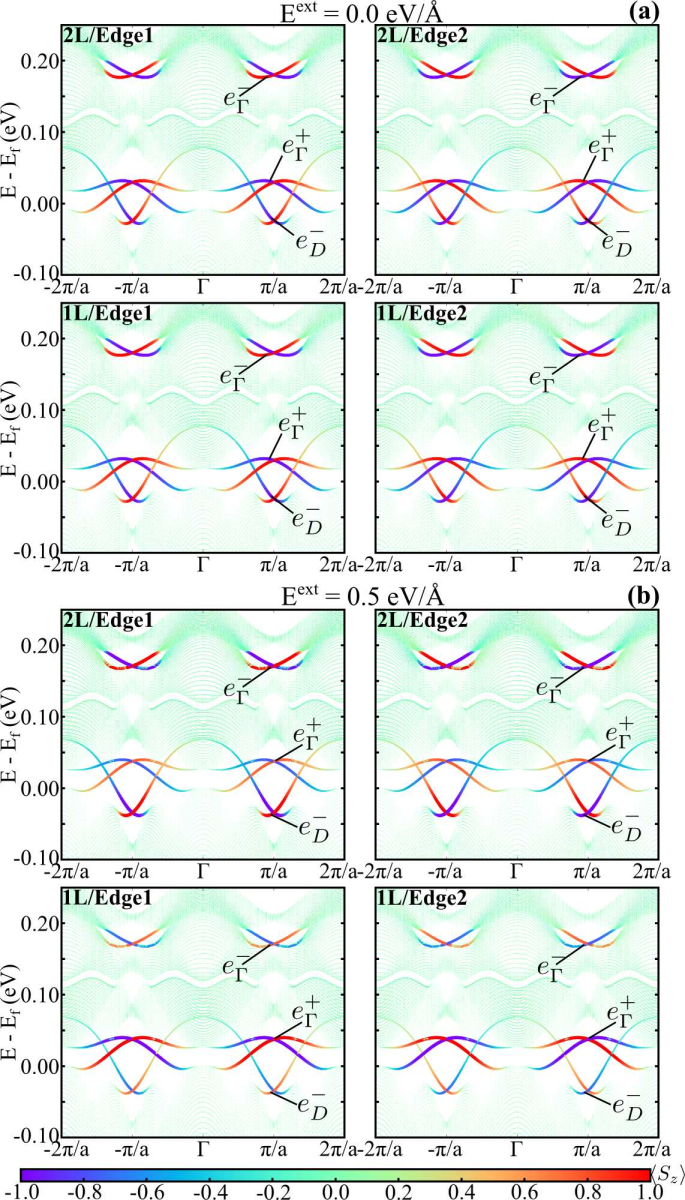
Edge states localized at opposite sides of the same (MC4S4)3 ML present opposite chiralities; while edge states of different MLs present the same chirality and the same electronic density of states. The latter is a consequence of the mirror symmetry in the BL systems. As we have shown in the previous section, the mirror symmetry can be removed by turning on an external electric field perpendicularly to the (MC4S4)3 layers. Here we will focus on the interlayer separation of the topological edge states mediated by an external electric field.
The effect of on the localization of the edge states are depicted in Figs. 6(b) and 7(b). In the former diagram we present the localization of the edge states in the (NiC4S-BL NR upon an external field of eV/Å. The edge states and are mostly localized on one ML (1L), while lies on the other (2L).
Similarly to what we have done in the BL systems, we can define a separation ratio for the edge states (). In order to compare with the calculated for (MC4S4)3-BLs, we will consider the (layer) projection of the edge states ,
We find for ( eV/Å), which is practically the same result obtained in (NiC4S-BL, at the same external field. As shown in Fig. 7(b), such a charge density separation also takes place in the (PtC4S-BL NR, however is not so effective. This is a consequence of the net charge transfer verified in (PtC4S-BL, as discussed above. Indeed, here we find , and , giving rise to , for eV/Å; which is practically the same value obtained in (PtC4S-BL, .
On the other hand, as shown in Fig. 4, the separation of the partial charge densities in (MC4S4)3-BLs can be tuned by changing the vertical distance between the (MC4S4)3 sheets. For instance, reduces from 0.67 to 0.19 by increasing the interlayer distance from 3.6 to 3.9 Å in (PtC4S-BL. Edge states in (PtC4S-BL NR present the same behavior. By increasing the interlayer distance to Å, the layer separation of the edge states is strengthened, where we find , and , , for eV/Å. That is, in addition to the external electric field, the interlayer distance is another degree of freedom which allow us to control the localization of the topologically protected edge states in (MC4S4)3 BL nanoribbons. It is worth to mention that such a control on the interlayer distance, between the organic layers, can be done through the current pillaring processes in MOFs Eubank et al. (2011); Sun et al. (2017).
IV Conclusion
Based on first-principles calculations and tight-binding model, we show that the energetic stability of the (MC4S4)3-BLs, M = Ni and Pt, is ruled by vdW interactions, being the AA stacking the most stable one. The electronic structure of the (MC4S4)3-BLs is characterized by the formation of bonding and anti-bonding KBSs; where the energy gaps in the KBSs, induced by the SOC, give rise to QSH or Z2-metallic state in (MC4S4)3-BLs. Their topologically non-trivial nature was identified through the formation of chiral spin-polarized edge states. By considering a phenomenological model, combined with first-principles calculations, we present a very comprehensive picture of the electronic properties upon the presence of an external electric field. In this case, the electronic contributions from each ML, to the formation of the bonding and anti-bonding KBSs, are no longer symmetric, with the bonding and anti-bonding KBSs localized in different MLs. We find that the chiral edge states follow the same pattern, and thus the localization of the topologically protected edge states in (MC4S4)3-BLs can be tuned by an external electric field. Our findings are not restricted to the (NiC4S and (PtC4S BLs. We can infer that such a tuning process will also take place in other mirror symmetric vdW metal-organic BLs characterized by a superposition of the kagome bands.
V ACKNOWLEDGMENTS
The authors acknowledge financial support from the Brazilian agencies CNPq, and FAPEMIG, and the CENAPAD-SP for computer time.
References
- Wang et al. (2013a) Z. F. Wang, Z. Liu, and F. Liu, Nat. Commun. 4, 1471 (2013a).
- Kambe et al. (2013) T. Kambe, R. Sakamoto, K. Hoshiko, K. Takada, M. Miyachi, J.-H. Ryu, S. Sasaki, J. Kim, K. Nakazato, M. Takata, and H. Nishihara, J. Am. Chem. Soc. 135, 2462 (2013).
- Wang et al. (2013b) Z. F. Wang, N. Su, and F. Liu, Nano Lett. 13, 2842 (2013b).
- Zhao et al. (2013) M. Zhao, A. Wang, and X. Zhang, Nanoscale 5, 10404 (2013).
- Yamada et al. (2016) M. G. Yamada, T. Soejima, N. Tsuji, D. Hirai, M. Dincă, and H. Aoki, Phys. Rev. B 94, 081102 (2016).
- Wang et al. (2013c) Z. Wang, Z. Liu, and F. Liu, Phys. Rev. Lett. 110, 196801 (2013c).
- Kim et al. (2016) H.-J. Kim, C. Li, J. Feng, J.-H. Cho, and Z. Zhang, Phys. Rev. B 93, 041404 (2016).
- Sheberla et al. (2014) D. Sheberla, L. Sun, M. A. Blood-Forsythe, S. Er, C. R. Wade, C. K. Brozek, A. Aspuru-Guzik, and M. Dinc, J. Am. Chem. Soc. 136, 8859 (2014).
- Pan et al. (2014) H. Pan, X. Li, Z. Qiao, C.-C. Liu, Y. Yao, and S. A. Yang, New J. Phys 16, 123015 (2014).
- Zhao et al. (2014) B. Zhao, J. Zhang, W. Feng, Y. Yao, and Z. Yang, Phys. Rev. B 90, 201403 (2014).
- Geim and Grigorieva (2013) A. K. Geim and I. V. Grigorieva, Nature 499, 419 (2013).
- Radisavljevic et al. (2011) B. Radisavljevic, A. Radenovic, J. Brivio, i. V. Giacometti, and A. Kis, Nat. Nanotech. 6, 147 (2011).
- Kitagawa et al. (2004) S. Kitagawa, R. Kitaura, and S.-i. Noro, Angew. Chem. Int. Ed. 43, 2334 (2004).
- Colson and Dichtel (2013) J. W. Colson and W. R. Dichtel, Nat. Chem. 5, 453 (2013).
- Zhang et al. (2014) M. Zhang, G. Feng, Z. Song, Y.-P. Zhou, H.-Y. Chao, D. Yuan, T. T. Tan, Z. Guo, Z. Hu, B. Z. Tang, et al., J. Am. Chem. Soc. 136, 7241 (2014).
- Rodriguez-San-Miguel et al. (2016) D. Rodriguez-San-Miguel, P. Amo-Ochoa, and F. Zamora, Chem. Commun 52, 4113 (2016).
- Sakamoto et al. (2016) R. Sakamoto, K. Takada, X. Sun, T. Pal, T. Tsukamoto, E. J. H. Phua, A. Rapakousiou, K. Hoshiko, and H. Nishihara, Coord. Chem. Rev. 320, 118 (2016).
- Adjizian et al. (2014) J.-J. Adjizian, P. Briddon, B. Humbert, J.-L. Duvail, P. Wagner, C. Adda, and C. Ewels, Nat. Commun. 5, 5842 (2014).
- Zhou (2014) J. Zhou, RSC Adv. 4, 13361 (2014).
- Kresse and Furthmller (1996) G. Kresse and J. Furthmller, Comput. Mater. Sci. 6, 15 (1996).
- Perdew et al. (1996) J. P. Perdew, K. Burke, and M. Ernzerhof, Phys. Rev. Lett. 77, 3865 (1996).
- Monkhorst and Pack (1976) H. J. Monkhorst and J. D. Pack, Phys. Rev. B 13, 5188 (1976).
- Blöchl (1994) P. E. Blöchl, Phys. Rev. B 50, 17953 (1994).
- Lee et al. (2010) K. Lee, E. D. Murray, L. Kong, B. I. Lundqvist, and D. C. Langreth, Phys. Rev. B 82, 081101 (2010).
- Tang et al. (2011) E. Tang, J.-W. Mei, and X.-G. Wen, Phys. Rev. Lett. 106, 236802 (2011).
- (26) See supplemental materials for more details of the methodology.
- Lü et al. (2017) T.-Y. Lü, H. Feng, S.-W. Yang, and J.-C. Zheng, Comput. Mater. Sci. 126, 170 (2017).
- Zhou et al. (2014) M. Zhou, Z. Liu, W. Ming, Z. Wang, and F. Liu, Phys. Rev. Lett. 113, 236802 (2014).
- Lebedeva et al. (2011) I. V. Lebedeva, A. A. Knizhnik, A. M. Popov, Y. E. Lozovik, and B. V. Potapkin, Phys. Chem. Chem. Phys. 13, 5687 (2011).
- Mostaani et al. (2015) E. Mostaani, N. Drummond, and V. Fal’ko, Phys. Rev. Lett. 115, 115501 (2015).
- Marom et al. (2010) N. Marom, J. Bernstein, J. Garel, A. Tkatchenko, E. Joselevich, L. Kronik, and O. Hod, Phys. Rev. Lett. 105, 046801 (2010).
- Gao and Tkatchenko (2015) W. Gao and A. Tkatchenko, Phys. Rev. Lett. 114, 096101 (2015).
- Eubank et al. (2011) J. F. Eubank, L. Wojtas, M. R. Hight, T. Bousquet, V. C. Kravtsov, and M. Eddaoudi, J. Am. Chem. Soc. 133, 17532 (2011).
- Sun et al. (2017) H. Sun, D. Lin, and Z. Gao, J. Porous Mater. 24, 291 (2017).
Supplemental Materials: Tuning the topological states in metal-organic bilayers
In the present Supplemental Material, we provide details of the TB model applied for the (MC4S4)3-ML/BL systems, Section I; describe the phenomenological Hamiltonian for mirror symmetric bilayers and the effect of breaking this mirror symmetry, Section II; and analyse the Rashba spin-orbit contribution to the topological phases of the (MC4S4)3-ML and BL, Section III. In this latter section, based on the TB model and first-principles calculations, we show that the Rashba spin-orbit contribution can be safely neglected in the present study.
VI Kagome Lattice Tight-Binding Model
The real-space tight-binding Hamiltonian of kagome-hexagonal lattice in the presence of intrinsic spin-orbit coupling (SOC) [S1, S2] can be written as
| (S1) |
where each term is given by
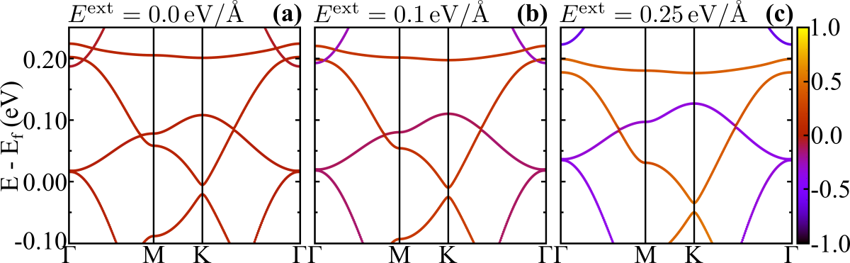
here, and are the creation and annihilation operators for an electron with spin on site ; the spin Pauli matrices, and the unity vector connecting the -th and j- sites to the -th nearest-neighbor in common [Fig. S1(a)], such that (where the proportionality constant is absorbed in ), and , the strength of hopping and spin-orbit terms. The and refer to nearest-neighbor and next nearest-neighbor summation, respectively. It worth to mention that we have done DFT first-principles calculation on the (MC4S4)3 monolayers (ML) with perpendicular external electric field up to eV/Å, in which we do not observe any Rashba SOC effect on the band structure. Therefore in our TB model we have taken the Rashba SOC as null [ more details on the Rashba SOC term in the last section].
The kagome lattice is given by a hexagonal lattice with 3 atoms as base [see main text, Fig.1]. For this lattice we can identify the nearest () and next nearest () neighbors in plane hopping, as represented in Fig.S1(a). By the formation of bilayer systems in addition to the in plane hopping, interlayer hopping are considered as represented in FIg. S1(b).
For (MC4S4)3-ML (M= Ni, Pt) we find a good TB description of the system by fitting the first-principles band structure with the parameters show in TABLE SI, considering a single orbital per kagome site. We can see that the single orbital TB Hamiltonian describe well the kagome band set (KBS) dispersion [Fig. S2(a1) and (b1)] obtained by DFT first-principles calculations [see main file methodology to DFT description].
| Parameter | (NiC4S | (PtC4S |
|---|---|---|
| 550.0 | 575.0 | |
| -38.0 | -40.0 | |
| -2.0 | -3.0 | |
| -1.8 | -4.7 | |
| -0.2 | -1.7 |
Within the TB hamiltonian we can track the evolution of Wannier Charge Center (WCC) of an effective 1D system. Where the topological invariant number is given by WCC evolution through half pumping cycle
| (S2) |
where , are for Kramers pairs, and are the index of occupied states in terms of pairs [S3, S4]. One graphical way to visualize the , is to draw a reference arbitrary vertical line from to on the WCC evolution, where even (odd) number of crossing with the reference line determine the topological trivial (non-trivial) characteristic of the system [S4].
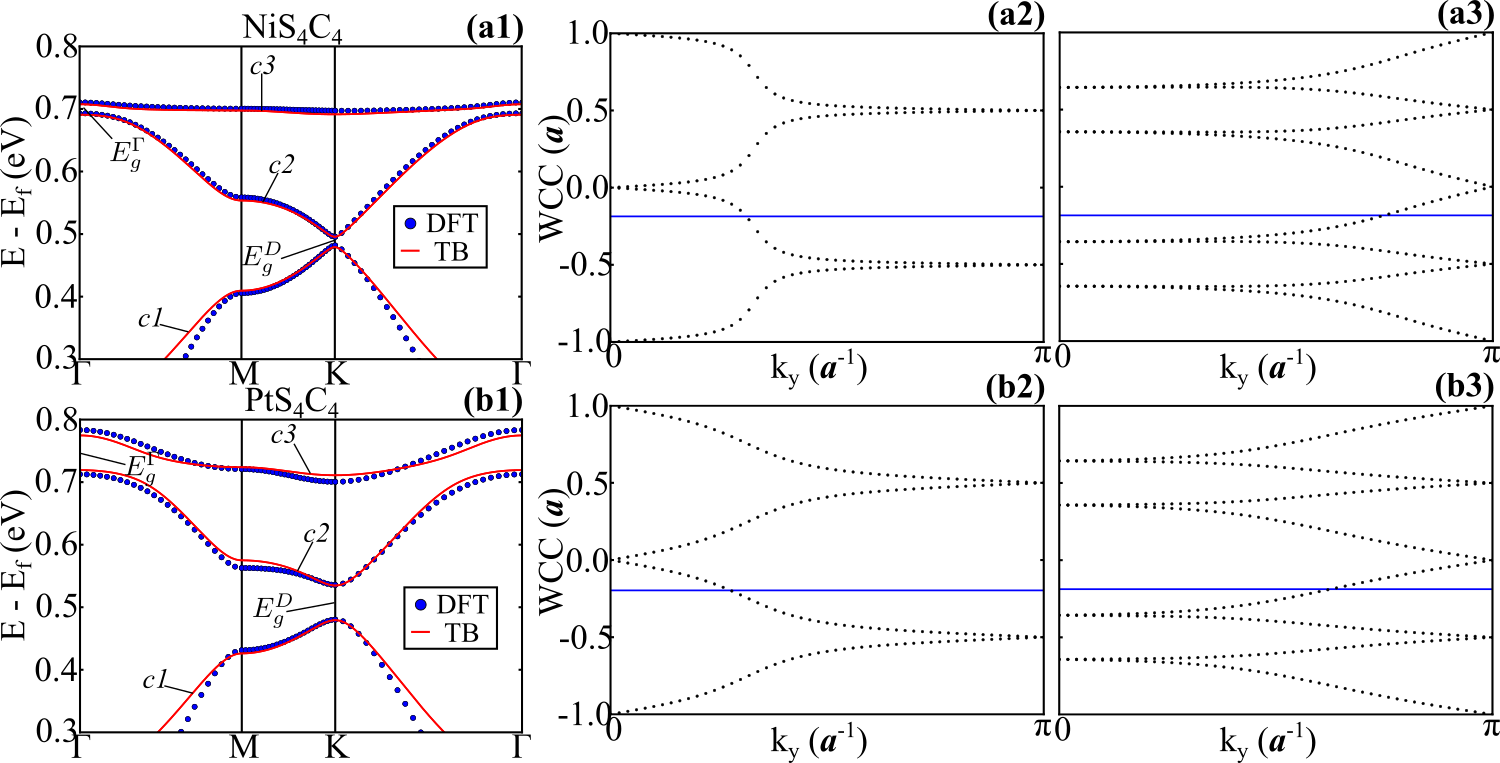
By considering the occupation of (MC4S4)3-ML up to , namely band fully occupied and , unoccupied [Fig. S2(a1) and (b1)], we can calculate the WCC of the system. As show in Fig. S2(a2) and (b2) for (NiC4S and (PtC4S], respectively, the reference line (blue solid line) cross the evolution line one time, therefore which characterizes this gap as topologically non-trivial. In a same way, for the occupation up to , namely and band fully occupied [Fig. S2(a1) and (b1)], the reference line cross the evolution line one time as show in Fig. S2(a3) and (b3) for (NiC4S and (PtC4S, respectively. We can conclude that both gaps and are topologically non-trivial, and making a lateral interface with a trivial material is expected a chiral edge state.
Next we have constructed nanoribbons of (MC4S4)3 with width (W) of nm, with three different edge geometries, Fig. S3(a), (b) and (c). Here are observed the formation of chiral edge states within the bulk SOC induced gap energy ( eV) and (). From Fig. S3(a) we can see that the ribbon geometry does not have inversion symmetry as we have two different type of edges, i. e. one terminated with a chain of atoms (Edge 1) and other by triangles (Edge 2). Within this asymmetric nanoribbon, each edge has a chiral momentum-spin locked states, degenerated at the time reversal invariant momenta (TRIM) in , but with different Fermi velocities. On the other hand, for the inversion symmetric nanoribbons, Fig. S3(b) and (c), the chiral states of opposite edges has the same Fermi velocity.
For the (MC4S4)3 bilayer TB model we considered two mirror symmetric kagome lattices. In addition to this doubled system we have considered two orbitals per kagome site (A and B), as the monolayer KBS below the Fermi level [see Fig. 2(a1) and (b1) in the main file] become relevant near the bilayer Fermi level. To discriminate the SOC and hopping strength for different orbitals we use the notation , meaning the th neighbor hopping between the orbital X and Y (with X,Y A,B), as presented in TABLE SII. This parameters well described the main characteristics of the first-principles band structure as show in Fig. 5(c) and (d) of the main file.
| Parameter | (NiC4S | (PtC4S | Parameter | (NiC4S | (PtC4S |
|---|---|---|---|---|---|
| 360.0 | 369.0 | -506.0 | -488.0 | ||
| 291.0 | 291.0 | -46.7 | -47.5 | ||
| -1.0 | -5.0 | -45.6 | -45.6 | ||
| 7.6 | 14.0 | 0.0 | 0.0 | ||
| 0.0 | 0.0 | -1.8 | -4.7 | ||
| -0.2 | -1.7 | -1.9 | -6.0 | ||
| -1.8 | -4.5 | 0.0 | 0.0 | ||
| 0.0 | 0.0 | -9.0 | -7.0 | ||
| 0.0 | 0.0 | -20.0 | -20.0 | ||
| 0.0 | 0.0 | 2.0 | 8.0 | ||
| -2.0 | -2.0 |
For the mirror symmetric (MC4S4)3-BL Hamiltonian, one can break the mirror symmetry by adding a potential difference between the layers through the on site energy of each layer orbital, i. e. making , with () sign for the upper (lower) layer. This potential difference can be due to an external electric field (). Taking (NiC4S-BL as an example, we can see that in the absence of external electric field [Fig. S4(a)] the system is mirror symmetric and each layer contribute equally to each state. On the other hand, by breaking the mirror symmetry the contribution of each layer to an given state are dependent, as show the color map fin Fig. S4(b) and (c). We introduce a phenomenological model to explain the effects of this mirror symmetry breaking, as discussed in the next section.
VII Phenomenological Model: (MC4S4)3-BL
Here we propose a phenomenological model to describe the interaction between the layers for the AA staking configuration. Firstly, knowing the Hamiltonian of each monolayer separately , diagonal on the base ( bands, layers), which gives each kagome band set (KBS) dispersions. Therefore, the general Hamiltonian for the two identical layers in the AA staking interacting with each other, and with an external electric field perpendicular to the layers is
| (S3) |
where () are the Pauli matrix in the layers space, is the coupling between the layers and the potential energy associated with the electric field. Here we omit the spin degree of freedom, since time-reversal is preserved. Also describe the asymmetry of the two layers upon presence of external electric field. If, on the presence of external electric field, the two layers does not exchange electrons, the potential energy between the layers is just (for in eV/Å), and defining , we have . On the other hand, if the presence of external electric field make the layers exchange electrons, the potential energy between the layers is weakened by the presence of a induced local electric field , therefore in this case , and for . The eigenvalues and eigenstates of this interacting layer model are given by
| (S4) |
| (S5) |
with
and the band index . Therefore we can write the energy separation between each KBS as .
If the electric field is absent () the Hamiltonian commutes with the mirror symmetry, such that the eigenvalues and eigenstates are
| (S6) |
| (S7) |
These solutions show us that: (i) for the band structure is composed by two KBS (symmetric and anti-symmetric ) separated in energy by (), and as long as the mirror symmetry is present, each state is an equal linear combination of the state from each layer (); on the other hand (ii) for the system present two fold degenerated KBS (regardless of spin).
In contrast, for the contribution of each layer to a given band is dependent, been and for the layer 1L and 2L, respectively. For these contributions are linear with ,
| (S8) | |||
| (S9) |
In Section I we have seen that each monolayer returns the topological invariant . Interestingly, the bilayer system also has . As shown above, for a mirror symmetric bilayer (), we find KBS states formed by bonding and anti-bonding orthogonal subspaces, which are energy split by [see Eqs. (S6)-(S7)]. These are eigenstates of the mirror symmetry with eigenvalues . Within each subspace, the topological invariant is . For a finite the mirror symmetry is broken. Nonetheless, it is still possible to label the KBS states by the orthogonal subspaces defined by the eigenstates of [see Eq. (S5)], with eigenvalues . This simply generalizes the mirror symmetry and yields for each subspace. Notice that for , reduces to the mirror symmetry operator, while for it labels the top and bottom layers, as shown in Fig. S4.
VIII Rashba Spin-Orbit Coupling
The contribution of the Rashba SOC on the electronic band structure of the (MC4S4)3-ML and -BL systems is defined by the term added to the tight-binding Hamiltonian
| (S10) |
where and are given in Eq.(S1), and
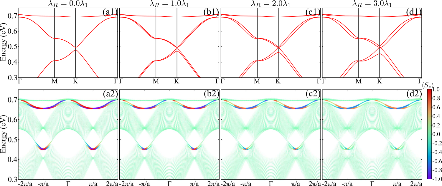
with the unitary vector connecting the -th to the -th site. The effect of Rashba SOC in the low energy Dirac dispersion of graphene is well known; the energy gap induced by intrinsic spin-orbit coupling vanish for large Rashba SOC contribution, characterized by a spin-splitting of the energy bands [S5, S6]. Here, we find a somewhat similar picture in the (MC4S4)3-ML and -BL. In Figs. S5(a1)-(d1) we present the energy bands of (MC4S4)3-ML as a function of the the strength of the Rashba SOC () in , , where we can identify the spin-splitting due to the Rashba SOC for . Further consequences on the edges states of (MC4S4)3 nanorribons, upon the inclusion of , are shown in Figs. S5(a2)-(d2). The edge states are preserved, however, their chiral spin polarizations fade out by increasing the Rashba SOC contribution (). It is interesting to note that even for large Rashba contribution, e.g. in Fig. S5(c), the (spin) chirality of the edge states has been preserved. In the sequence, based on first-principles calculations, we will show that the contributions of the Rashba SOC are quite small in the present (MC4S4)3-ML and BL systems.
An external electric field perpendicular to the (MC4S4)3 layers suppresses the mirror of the system, and thus promoting the Rashba SOC effects. In order to provide a quantitative measure of such a contribution on the (NiC4S and (PtC4S-ML and -BL systems, we perform a set of first-principles calculations of the electronic band structures of those (MC4S4)3 systems upon the presence of an external electric field (). In Figs. S6(a1)-(c1) and S6(a2)-(c2) we present the electronic band structure of (NiC4S- and (PtC4S-MLs for eV/Å; where we find that the effect of Rashba SOC is much smaller compared with the one of the intrinsic SOC, up to eV/Å. For instance, the (NiC4S-ML exhibits a a spin-splitting of about meV for eV/Å, which is small in comparison with the (intrinsic SOC) energy gap of meV (less than ), Fig. S6(d1). Similarly, in (PtC4S-ML, we found a spin-splitting of 5 meV and an energy gap of 60 meV due to the intrinsic SOC, Fig. S6(d2).
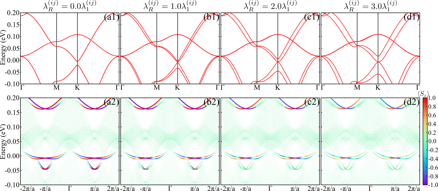
Following the same scheme, based on the TB model [Eq. (S10)], in Figs. S7(a1)-(d1) we present the electronic band structures of the (MC4S4)3-BL, as a function of the strength of the contribution (), and the respective spin-polarized edge states, Figs. S7(a2)-(d2). Similarly to what we found in the single layer systems, (i) the spin-chirality of the edges fades out for larger values of in comparison with , however (ii) even for , the chiral character of the (edge) energy bands has been maintained. In the sequence, we performed first-principles calculations of the electronic band structures of (NiC4S-BL and (PtC4S-BLs as a function of the external electric field. Our results are summarized in Fig. S8, where we show the evolution of the electronic band structures of (NiC4S-BL (a1)-(c1) and (PtC4S-BL (a2)-(c2). For both systems, we found that the spin-splitting due to the Rashba SOC about ten times smaller than the energy gap induced by the intrinsic SOC, Figs. S8(d1) and (d2).
Therefore, we can infer that the effect of Rashba SOC is small, compared with the other contributions, and can be dismissed in the (present) (MC4S4)3 monolayer and bilayer systems for within the studied range.
[S1] E. Tang, J.-W. Mei, and X.-G. Wen, Phys. Rev. Lett. 106, 236802 (2011).
[S2] Z. Wang, Z. Liu, and F. Liu, Phys. Rev. Lett. 110, 196801 (2013).
[S3] A. A. Soluyanov and D. Vanderbilt, Phys. Rev. B 83, 235401 (2011).
[S4] R. Yu, X. L. Qi, A. Bernevig, Z. Fang, and X. Dai, Phys. Rev. B 84, 075119 (2011).
[S5] M. Gmitra, S. Konschuh, C. Ertler, C. Ambrosch-Draxl, and J. Fabian, Phys. Rev. B 80, 235431 (2009).
[S6] C. L. Kane and E. J. Mele, Phys. Rev. Lett. 95, 146802 (2005).