Transport and optics at the node in a nodal loop semimetal
Abstract
We use a Kubo formalism to calculate both A.C. conductivity and D.C. transport properties of a dirty nodal loop semimetal. The optical conductivity as a function of photon energy , exhibits an extended flat background as in graphene provided the scattering rate is small as compared to the radius of the nodal ring (in energy units). Modifications to the constant background arise for and the minimum D.C. conductivity which is approached as as , is found to be proportional to with the Fermi velocity. For we recover the known three-dimensional point node Dirac result while for , becomes independent of (universal) and the ratio where all reference to material parameters has dropped out. As is reduced and becomes of the order , the flat background is lost as the optical response evolves towards that of a three-dimensional point node Dirac semimetal which is linear in for the clean limit. For finite there are modifications from linearity in the photon region . When the chemical potential (temperature ) is nonzero the D.C. conductivity increases as () for . Such laws apply as well for thermal conductivity and thermopower with coefficients of the quadratic law only slightly modified from their value in the three-dimensional point node Dirac case. However in the limit both have the same proportionality factor of as does . Consequently the Lorentz number is largely unmodified. For larger values of away from the nodal region the conductivity shows a Drude like contribution about which is followed by a dip in the Pauli blocked region after which it increases to merge with the flat background (two-dimensional graphene like) for and to the quasilinear (three-dimensional point node Dirac) law for .
pacs:
72.15.Eb, 78.20.-e, 72.10.-dI Introduction
Optical (IR) along with other spectroscopies such as angular resolved photo emission ARPES and scanning tunelling microscopy have given us a wealth of information on the dynamics of charge carriers in metals and superconductors Carbotte ; Basov ; Jiang with different gap symmetries. More recently the dynamic optical conductivity as a function of temperature and photon energy has been equally successful when applied to the class of two-dimensional (2D) metals such as graphene Li ; Stille ; Sharapov , the surface states of topological insulators Schafgans ; Zhou as well as topological materials such as Dirac and Weyl semimetals Chen ; Sushkov ; Xu ; Neubauer ; Timusk ; Chinotti ; Tabert ; Nicol ; Carbotte1 .
Another recent development has been the discovery of nodal loop semimetals Burkov ; Aji ; Carter ; Kim ; Weng ; Uchoa ; Fang ; Bian ; Yamakage ; Araújo ; Ezawa . Their magnetic susceptibility Koshino , density fluctuation plasmons and Friedel oscillationsRhim , Landau quantization YBKim and some aspect of their topological electrodynamic response Ramamurthy have been studied. The dynamical optical conductivity as a function of photon energy has also been considered in the clean limit Carbotte2 . It was found to display signatures of both three-dimensional (3D) point node Weyl or Dirac-like materials and 2D graphene-like systems, depending on what range of photon energy is used to probe the dynamics. For small compared with twice the radius in energy units of the nodal ring(), the response is 2D in nature while for it evolves to 3D, characteristic of point node Dirac. In any realistic case, the charge carriers will also have a finite scattering rate which influences their motion. In this paper we study the effect of on the electromagnetic properties of a nodal loop semimetal at finite chemical potential and photon energy. In addition, we consider D.C. transport including conductivity, thermal conductivity, thermopower and Lorentz number. Here we will be particularly but not exclusively interested in the case when the chemical potential and temperature T are small compared with which allows optics and transport at the nodes to be probed. This regime includes the concept of minimum conductivity and how it is modified when and/or T is increased out of zero.
In section II we present the necessary formalism including the Kubo formula for the dynamical conductivity at finite T and photon energy. Results at finite photon energy are given in section III. While many of our results are for (nodal region) the effect of a finite chemical potential are also presented. In section IV we consider D.C. properties, electrical conductivity, thermal conductivity, thermopower and Lorentz number. A discussion and conclusion can be found in section V.
II Formalism
The continuum matrix Hamiltonian for a loop node semimetal on which our work is based takes the form
| (1) |
where is the Fermi velocity, is the momentum equal to and b is a Zeeman field oriented along the -axis. The matrix and are each a set of Pauli matrices. For convenience in our calculation we will set and only at the end restore them. The energies of the two sets of bands involved can be written as,
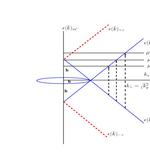
| (2) |
where and . The index gives conduction () and valence () band associated with the dispersion curves of the band. These dispersion curves are highlighted in Fig. 1.
The component of the dynamical conductivity which can be calculated from the Kubo formula, depends on the spectral density of the charge carriers and takes the form,
| (3) |
for the interband transitions () and the intraband part () is given by the formula
| (4) |
In terms of the carrier self energy , the spectral functions take the form Sharapov ,
| (5) |
For simplicity in our calculation we will take the case of residual scattering modeled through a constant imaginary part . We will consider two limiting cases for Eq. (II). The D.C. limit of in which instance the thermal factor
| (6) |
where is the Fermi-Dirac thermal distribution function. The zero temperature case for which the integral over becomes limited to the range to where is the chemical potential and the thermal factor is to be replaced by 1.
The limit involves an integral over of the form
| (7) |
which can be done analytically and gives,
| (8) |
where we have introduced polar coordinates for variables and have divided all variables by the scattering rate which has had the effect of scaling out . Of course it remains in and while the other variables are dummies of integration. The function has the form
| (9) |
An equivalent equation can be derived for the intraband case. We obtain,
| (10) |
with
| (11) |
We have checked that these equations properly reduce to the clean limit forms for used in the work of Ref.[Carbotte2, ] with which we will compare when appropriate.
III Results for finite frequencies
In Fig. 2 we show our results for the zero temperature dynamic optical response as a function of photon energy both quantities normalized by the optical scattering rate i.e. vs. . In these reduced variables has dropped out and we have a single set of curves which apply for any value of . In fact we have a family of curves defined by two external parameters, the normalized chemical potential and nodal loop parameter . Here represents charge neutrality and we consider nine values of . Starting from the top curve we see a graphene like 2D constant background extending from a bit above of all the way to at which point it shows a transition to a linear in behavior characteristic of a 3D point node Dirac material. The height of this plateau referred to as the interband background Gusynin and denoted by agrees (after a correction of a dropped factor of 2) with the value obtained in Ref.[Carbotte2, ] where the clean limit was considered. At however our new results show a bend downward to connect with the D.C. value of the conductivity as we will discuss shortly. As the value of the nodal loop parameter is reduced towards zero the frequency range over which a plateau is well defined shrinks. It is still seen in the dashed blue curve for but below this value we see a clear evolution from a constant value to linear like behavior characteristic of a 3D Dirac point node system as we will elaborate upon in Fig. 4. First we return to the limit. As we will see later (Eq. 20) we get a particularly simple and important result
| (12) |
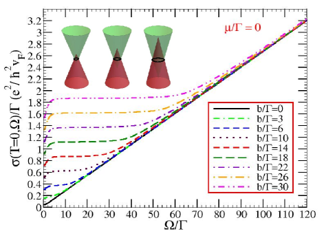
In the limit which here corresponds to a 3D point node Dirac model we get the known answer obtained in Ref.[Nicol, ], namely the minimum conductivity is not universal but rather depends linearly on optical scattering rate ( tewice the quasiparticle rate ). This is a very different result from that obtained for graphene Sharapov for which is simply a number in the same constant approximation used here and referred to as the universal interband background (). We see however from Eq. 12 that in the nodal loop semimetal drops out of if and in that case we get no dependence on scattering rate so is again universal equal to . While this minimum conductivity does not depend on it is linear in and inversely dependent on which are material dependent properties. In graphene no such material parameters arise Sharapov . A universal conductivity Lee is also part of d-wave Jiang superconductivity theory. It arises when a gap which can have complex symmetry Donovan ; Donovan1 nevertheless goes through a zero Yip ; Schachinger on the Fermi surface. It does not arise in an s-wave superconductor even if there is some anisotropy such as in AlLeung but with no zero. We note that the magnitude of minimum conductivity depends on the model used for the disorder as discussed in the review of Evers and Mirlin [Mirlin, ] for the specific case of graphene. Here only the simplest model of constant scattering was used.
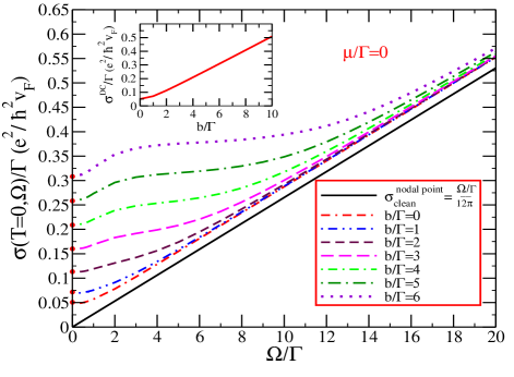
The approach to the minimum D.C. conductivity and more generally the transition from 2D graphene like behavior for the A.C. conductivity to 3D point node Dirac behavior as gets small is further elaborated upon in Fig. 3. Again we show the photon energy dependence of the zero temperature conductivity both normalized by so as to get universal curves but here we consider only values of less than (dotted violet curve). While this curve still shows a clear tendency to flatten out in the region around , the other results do not. By the curve for vs is convex upward and no trace of a plateau remains. The dot-double-dashed red curve for reproduces the results of Ref.[Nicol, ] for a 3D Dirac point node semimetal. We have also placed on the same graph their results (solid black curve) for the clean limit. A straight line of slope applies in this case . In the inset to Fig. 3 we show the evolution of minimum D.C. conductivity normalized to as a function of from Eq. 12, which in our units is . We see that it rapidly goes from a constant to linear in and inversely proportional to . These results are plotted on the axis of the main frame as heavy red dots.
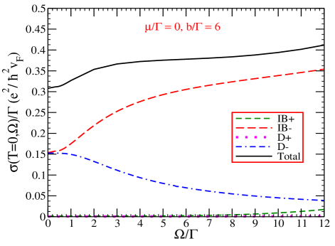
It is important to understand that when residual scattering (finite ) is introduced both interband and intraband optical transition contribute to the minimum conductivity Eq. 12 as they do to finite photon energy properties. This is illustrated in Fig. 4 where we treat the specific case , for definiteness. We have decomposed the contributions to into four terms. The dashed green line is the interband (IB) contribution of the band and the dashed red line is for , the dotted magenta line is the intraband (D) contribution with and the double-dashed-dotted blue line for . It is clear and expected that the band contributes little to the conductivity in the region because it is gaped as can be seen in Fig. 1. In fact if we had not included some scattering () these contributions would be identically zero in the clean limit. Even for it is the that gives almost the entire contribution from interband (dashed red curve) and intraband (double-dashed-dotted blue curve) optical transitions. Note that at (D.C. limit) both give exactly the same contribution. This is entirely due to the presence of finite . In the clean limit there is no intraband conductivity because the chemical potential in our example and the entire D.C. conductivity comes from the interband transitions. Thus scattering has a profound effect on these results.
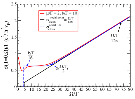
In Fig. 5 we elaborate further on the relationship of our results to the clean limit results of Ref.[Nicol, ; Carbotte2, ]. What is shown as the solid red curve is normalized with in units of as a function of for a case and . In this example a Drude like peak is clearly seen in the vicinity of . This contribution would exists even in the clean limit but would take the form of a Dirac delta function at . For comparison with the clean limit we also show as solid blue line the clean limit result of reference Ref.[Carbotte2, ] corrected for a missing factor of 2. We have,
| (13) |
with
| (14) |
This is plotted as blue solid line (labeled as ) which is cut off below because interband optical transition are not possible below this photon energy because of Pauli blocking (see Fig. 1). The optical spectral weight lost is of course transferred to a delta function at not shown on the figure. Having understood that at finite this spectral weight is distributed into a Drude like form around we see that the clean limit results agree very well with our new results for the finite case (solid red curve). We have also placed for additional comparison the results of Ref.[Nicol, ] for point node Dirac as a solid black curve which is a straight line of slope . It too is to be cut off at . While it matches well with the other two curves in the large region it is very different from the nodal loop results below .
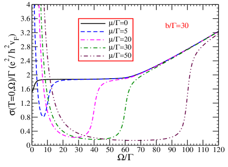
In Fig. 6 we present additional results for the case of finite chemical potential. Here is fixed at 30, and five values of are considered. The solid black line is for and has already been presented in Fig. 2 as dashed-double-dotted magenta line. It is repeated here for comparison. The finite curves all shows a large Drude like peaks at small photon energies. Beyond this Drude, all curves show a depression in conductivity before rising up again to meet the curve at higher energies. The dashed blue curve for has only a small dip and has recovered to its value by ; which is twice the value of , the low energy cut off on interband transition that would apply to the clean limit. Here this cutoff is no longer sharp because of the smearing caused by disorder (finite ). When the chemical potential is increased to (double-dashed-dotted magenta curve) the conductivity displays a much more pronounced dip beyond the Drude region of photon energy. In the clean limit we would have had a large delta function contribution at than a complete zero up to after which it would have recovered its plateau value. Disorder smearing has partially filled in the gap region and has also smeared the edge at . At still higher values of the same behavior is observed but at large the conductivity goes back to the linear law of 3D point node Dirac.
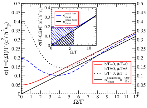
One interesting special case with some additional commentary is the case . In the clean limit this corresponds to the transfer of the entire optical spectral weight from the flat 2D graphene like plateau in the interband conductivity to the intraband delta function at . This leave a region above which would deviate very little from the straight line of slope of 3D point node Dirac. Nevertheless the two cases can be differentiated from each other when as is shown in Fig. 7. The black dotted line is the result for with as well. We see that the disorder smearing has broaden the intraband transition contribution to such an extent that no Pauli blocking gap is seen at . This is also true for the dashed blue curve obtained when is set to zero. This curve does differ from the black dotted curve when is included. The main reason for this is that the optical spectral weight under the Drude is very different in the two cases as is illustrated in the inset of the figure. The shaded region shows the lost optical spectral weight (OSW) in the interband background that has been transferred to the intraband. In the clean limit we have for the nodal loop and for the 3D point node Dirac. The ratio of the loop to point node is . Thus there is more than a factor of 2 difference between these two quantities and this leads to the striking differences between dotted black and dashed blue curves of the main frame of Fig. 7 in the region of photon energy below twice the value of the chemical potential. Above both curves are the same and are not very different from the solid red curve for (3D point node Dirac) including finite and from the solid black curve which is the clean limit version of the solid red curve included for comparison.
IV D.C. Transport
The D.C. limit of Eq. (II) gives
| (15) |
for the interband contribution and
| (16) |
for the intraband or Drude contribution. At zero temperature the thermal factor reduces to a delta function of the form which pins to be at the chemical potential. Eq. (IV) and (IV) then reduce to 2D integrals over and which are the integration variables introduced in Eq. (8). We get,
| (17) |
and
| (18) |
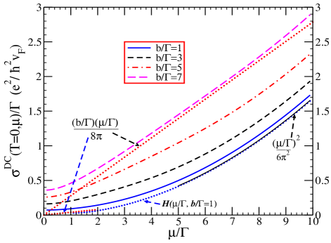
Results for are given in Fig. 8 where we plot
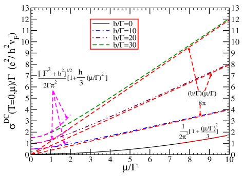
in units of as a function of for various values of namely solid black curve, dashed-dotted blue, double-dotted-dashed brown and dashed green. The solid black line is known from the 3D point node case Nicol and is
| (19) |
The limit of zero chemical potential gives
| (20) |
In this case the sum of Eq. (IV) and (IV) is particularly simple and the terms in Eq. (IV) and in Eq. (IV) add to give 1. We get,
| (21) |
which can be done analytically and gives Eq. (20). The implications of Eq. (20) were discussed in the previous section. Here we note that except for the curve increases linearly with b in Fig. 8 because . We shall also show below that for finite but , increases as out of its value. This behavior is indicated by a dashed magenta curve which agrees with our full numerical results at small but deviation occur as increases. In fact, for the finite curves there is a gradual evolution to a linear in dependence of which is characteristic of 2D graphene like behavior as obtained in Ref.[Carbotte2, ] for the clean limit. Here the clean limit corresponds to and large (). For , the clean limit result is
| (22) |
which is shown in Fig. 8 as the dashed red lines that go through the origin. The main difference between clean limit results and those that included carrier scattering are at small values of (near charge neutrality). Including a finite changes the dependence of the D.C. conductivity from linear in to a quadratic dependence in the region . By contrast the solid black curve for follows a quadratic law over the entire range shown. The evolution from quadratic to linear behavior is studied in more detail in Fig. 9 where small values of are considered namely (solid blue), (dashed black), (dashed-dotted red) and (dashed magenta) curves. Also shown on the figure for comparison are clean limit results (dotted blue) for and (dotted red) for . What is plotted for the dotted blue line are the result for the clean limit from Ref.[Carbotte2, ] (again corrected for a missed factor of 2). The relevant function is,
| (23) |
with
| (24) |
For , of Eq. (IV) reduces to which is independent of b and the result for 3D point node Dirac. It is clear that there are three regimes for . A linear regime for , a transition regime for during which evolves from a linear to quadratic dependence on and a final regime where the quadratic law holds. The size of relative to is critical in determining which regime is relevant for a particular value of . Note that in Fig. 8 the three curves with finite all fall in the regime and so only the linear region of is probed. In Fig. 9 however we have chosen such that the dotted blue curve (clean limit) ranges over all three regimes involved in as ranges from to . Below we are in the linear regime (dotted red curve) and above in the quadratic regime (solid black curve) with a transition region from linear to quadratic between these two extremes. For the dashed magenta curve however we do not show but rather have chosen to show only the linear dependence even outside its range of validity. It is clear that significant deviations from linearity for large values of enter only for . Comparing the case of finite with its clean limit (dotted curves) we see that the largest effect of finite is in the region where carrier scattering changes the linear law to a quadratic law.
We now turn to the small limit of and obtain analytically the law seen in Fig. 8. In fact it is convenient to return to Eq. (IV) and Eq. (IV) and include at the same time finite temperature effects. We take and in which case it is justified to expand the integrand of Eq. (IV) and Eq. (IV) to second order in dropping all higher order terms. After straightforward algebra we get that the D.C. conductivity takes the form
| (25) |
where
| (26) |
and with
| (27) | |||||
and
| (28) |
These integrals can all be done analytically to yield
| (29) |
The limit of corresponds to 3D point node Dirac. The D.C. conductivity reduces to
| (30) |
which is a function of and valid for both these variables less than one because of our expansion in to second order only. The D.C. conductivity is further linearly proportional to . Expression (30) agrees with the previous work Nicol in this limit. For a general and we get
| (31) |
with
| (32) |
which is always near 1 in value. Its minimum is at where it is , reduced from one by . While the value of is very different in the nodal loop case from the 3D Dirac point node case, the first going like while the second goes like , it has the same and dependence. T coefficient of this dependence is however always close to that of the point node Dirac.
Other important transport coefficients can also be calculated for . The formula for the conductivity is,
| (33) |
To get thermal conductivity() we drop the and add a factor of which gives . The total thermal conductivity has a thermopower correction and reads,
| (34) |
where the formula for the coefficient is given as in Eq. (33) without the and a factor added to the integral of the energy integration over . In terms of the thermopower is given by,
| (35) |
Another quantity often discussed is the Lorentz number () of the Wiedemann-Franz law. By definition,
| (36) |
It is straightforward to obtain explicit results for the above coefficients using algebra closely related to that of Appendix B of Ref. [Nicol, ]. The results are,
| (37) |
| (38) |
| (39) |
with a correction to for thermopower of the form . As we have seen for the point node Dirac case. For the nodal loop case is somewhat reduced going like for . When the disorder scattering rate becomes large as compared with we find that is reduced by at after which it again rises towards one. These results are only valid for and near charge neutrality.
The approach to the minimum D.C. conductivity for but with finite as is also of interest. It takes on the form of Eq. (31) with the second term in the square bracket replaced by . The expansion of the functions of Eq. (II) and of Eq. (II) in powers of and retaining terms to only gives,
| (40) |
where we needed to evaluate the integral,
| (41) |
V Conclusion
We have considered the effect of a finite scattering rate () on the finite frequency () electromagnetic response of a nodal loop semimetal and on its D.C. electrical conductivity, thermal conductivity, thermopower(or Seebeck coefficient) and Lorentz number (or Wiedemann Franz law). For the dynamic optical conductivity at zero temperature several regime arises as a function of even when the chemical potential is set equal to zero. In the limit of which corresponds to the minimum D.C. () conductivity we find where is the radius of the nodal ring in energy units, is the electron charge, the Plank’s constant and the Fermi velocity. This reduces to the known result for 3D point node Dirac when and to the clean limit result for a nodal semimetal when . In this last instance the correction for finite is of the order of . The approach to the minimum D.C. conductivity obeys a law with coefficient . This result agrees with the point node Dirac case of Ref. [Nicol, ] when . At frequencies a few times but smaller than we find a constant interband background as in graphene of height provided so that the ratio of and is exactly the same as one would get for graphene in the same constant approximation as used here. Of course both and are themselves different in that they both involve material parameters namely and while in graphene these drop out entirely of both properties. In the limit of the constant background loses its integrity and the conductivity evolves toward its behavior in 3D Dirac point node semimetal. For , again takes on the characteristic linear in dependence and in fact the parameter completely drops out.
For finite value of the chemical potential a Drude like response is obtained in the regime with width related to the scattering rate . In the pure case () the region up to would have zero conductivity but now this region shows only a depressed conductivity because of the disorder scattering. Beyond the flat background of the case is recovered if while we recover the linear dependence of the 3D point node Dirac case if with some smearing in the transition region around . Finite chemical potential also affects the behavior of D.C. properties. For the electrical conductivity we find that provided (or temperature ) is less than the approach to charge neutrality is quadratic in (). We have also considered the limit of large at and find the quadratic behavior characteristic of the dirty limit approach to charge neutrality and then gradually goes into a linear law characteristic of a 2D graphene like system when is much larger than and this changes to a law for .
Finally the D.C. thermal conductivity is found to vary as when , and have a or correction for , finite but smaller than one. The coefficient of these quadratic dependence are only slightly modified from the point node case. The maximum correction for finite is of order . This implies that the Wiedemann-Franz law is only very slightly change from its value for (point node case). A similar situation holds for the thermopower. We hope that our calculations will stimulate experimental studies of the optical and transport properties of nodal loop semimetals. In particular A.C. spectroscopic data can provide a wealth of valuable information on the dynamics of the charge carrier. Several such studies already exist for related systems of Dirac and Weyl semimetals Chen ; Sushkov ; Xu ; Neubauer ; Chinotti .
Acknowledgments
Work supported in part by the Natural Sciences and Engineering Research Council of Canada (NSERC) and by the Canadian Institute for Advanced Research (CIAR).
References
- (1)
- (2) J. P. Carbotte, T. Timusk, and J. Hwang,“Bosons in high-temperature superconductors: an experimental survey,” Reports on Progress in Physics. 74, 066501 (2011).
- (3) D. N. Basov and T. Timusk,“Electrodynamics of high-Tc superconductors,” Rev. Mod. Phys. 77, 721 (2005).
- (4) J. P. Carbotte, C. Jiang, D. N. Basov, and T. Timusk,“ Evidence for d-wave superconductivity in YBa2Cu3O7−δ from far-infrared conductivity,” Phys. Rev. B 51, 11798 (1995).
- (5) Z. Q. Li, E. A. Henriksen, Z. Jiang, Z. Hao, M. C. Martin, P. Kim, H. L. Stormer, and D. N. Basov,“Dirac charge dynamics in graphene by infrared spectroscopy,” Nature Phys. 4, 532 (2008).
- (6) L. Stille, C. J. Tabert, and E. J. Nicol,“Optical signatures of the tunable band gap and valley-spin coupling in silicene,” Phys. Rev. B 86, 195405 (2012).
- (7) J. P. Carbotte, E. J. Nicol, and S. G. Sharapov,“ Effect of electron-phonon interaction on spectroscopies in graphene,”Phys. Rev. B 81, 045419 (2010).
- (8) A. A. Schafgans, K. W. Post, A. A. Taskin, Yoichi Ando, Xiao-Liang Qi, B. C. Chapler, and D. N. Basov, “Landau level spectroscopy of surface states in the topological insulator BiSb via magneto-optics,”Phys. Rev. B 85, 195440 (2012).
- (9) Zhou Li and J. P. Carbotte,“ Optical spectral weight: Comparison of weak and strong spin-orbit coupling,”Phys. Rev. B 91, 115421 (2015).
- (10) R. Y. Chen, S. J. Zhang, J. A. Schneeloch, C. Zhang, Q. Li, G. D. Gu, and N. L. Wang,“Optical spectroscopy study of the three-dimensional Dirac semimetal ZrTe5,” Phys. Rev. B 92, 075107 (2015).
- (11) A. B. Sushkov, J. B. Hofmann, G. S. Jenkins, J. Ishikawa, S. Nakatsuji, S. Das Sarma, and H. D. Drew,“ Optical evidence for a Weyl semimetal state in pyrochlore Eu2Ir2O7,”Phys. Rev. B 92, 241108(R) (2015).
- (12) B. Xu, Y. M. Dai, L. X. Zhao, K. Wang, R. Yang, W. Zhang, J. Y. Liu, H. Xiao, G. F. Chen, A. J. Taylor, D. A. Yarotski, R. P. Prasankumar, and X. G. Qiu, “Optical spectroscopy of the Weyl semimetal TaAs,” Phys. Rev. B 93, 121110(R), (2016).
- (13) D. Neubauer, J. P. Carbotte, A. A. Nateprov, A. Löhle, M. Dressel, and A. V. Pronin, “Interband optical conductivity of the [001]-oriented Dirac semimetal Cd3As2,”Phys. Rev. B 93, 121202 (2016).
- (14) T. Timusk, J. P. Carbotte, C. C. Homes, D. N. Basov, and S. G. Sharapov, “Three-dimensional Dirac fermions in quasicrystals as seen via optical conductivity,” Phys. Rev. B 87, 235121 (2013).
- (15) M. Chinotti, A. Pal, W. J. Ren, C. Petrovic, and L. Degiorgi,“Electrodynamic response of the type-II Weyl semimetal YbMnBi2,” Phys. Rev. B 94, 245101 (2016).
- (16) C. J. Tabert, and J. P. Carbotte,“Optical conductivity of Weyl semimetals and signatures of the gapped semimetal phase transition,” Phys. Rev. B 93, 085442 (2016).
- (17) C. J. Tabert, J. P. Carbotte, and E. J. Nicol,“Optical and transport properties in three-dimensional Dirac and Weyl semimetals,” Phys. Rev. B 93, 085426 (2016).
- (18) J. P. Carbotte,“Dirac cone tilt on interband optical background of type-I and type-II Weyl semimetals,” Phys. Rev. B 94, 165111 (2016).
- (19) A. A. Burkov, M. D. Hook, and Leon Balents,“Topological nodal semimetals,” Phys. Rev. B 84, 235126 (2011).
- (20) M. Phillips and V. Aji,“Tunable line node semimetals,” Phys. Rev. B 90, 115111 (2014).
- (21) J.-M. Carter, V. V. Shankar, M. A. Zeb, and H.-Y. Kee,“Semimetal and Topological Insulator in Perovskite Iridates,” Phys. Rev. B 85, 115105 (2012).
- (22) Y. Kim, B. J. Wieder, C. L. Kane, and A. M. Rappe, “Dirac Line Nodes in Inversion-Symmetric Crystals,”Phys. Rev. Lett. 115, 036806 (2015).
- (23) H. Weng, Y. Liang, Q. Xu, R. Yu, Z. Fang, X. Dai, and Y. Kawazoe,“Topological node-line semimetal in three-dimensional graphene networks,” Phys. Rev. B 92, 045108 (2015).
- (24) Kieran Mullen, Bruno Uchoa, and Daniel T. Glatzhofer,“Line of Dirac Nodes in Hyperhoneycomb Lattices,” Phys. Rev. Lett. 115, 026403 (2015); Lilia S. Xie, L. M. Schoop, E. M. Seibel, Q. D. Gibson, W. Xie, and R. J. Cava,“A new form of Ca3P2 with a ring of Dirac nodes,” APL Materials. 3, 083602 (2015).
- (25) C. Fang, Y. Chen, H.-Y. Kee, and L. Fu,“Topological nodal line semimetals with and without spin-orbital coupling,” Phys. Rev. B 92, 081201(R) (2015).
- (26) G. Bian, T.-R. Chang, R. Sankar, S.-Y. Xu, H. Zheng, T. Neupert, C.-K. Chiu, S.-M. Huang, G. Chang, I. Belopolski, D. S. Sanchez, M. Neupane, N. Alidoust, C. Liu, B. Wang, C.-C. Lee, H.-T. Jeng, C. Zhang, Z. Yuan, S. Jia, A. Bansil, F. Chou, H. Lin and M. Z. Hasan,“Topological nodal-line fermions in spin-orbit metal PbTaSe2,” Nature Communications 7, 10556 (2016).
- (27) A. Yamakage, Y. Yamakawa, Y. Tanaka, and Y. Okamoto,“Line-Node Dirac Semimetal and Topological Insulating Phase in Noncentrosymmetric Pnictides CaAgX (X = P, As),” J. Phys. Soc. Jpn. 85, 013708 (2016).
- (28) L. Li and M. A. N. Araújo,“Topological insulating phases from two-dimensional nodal loop semimetals,” Phys. Rev. B 94, 165117 (2016); K. -H. Ahn, K. -W. Lee, and W. E. Pickett,“Spin-orbit interaction driven collective electron-hole excitations in a noncentrosymmetric nodal loop Weyl semimetal,’ Phys. Rev. B 92, 115149 (2015).
- (29) M. Ezawa,“ Loop-Nodal and Point-Nodal Semimetals in Three-Dimensional Honeycomb Lattices,”Phys. Rev. Lett. 116, 127202 (2016).
- (30) M. Koshino and I. F. Hizbullah,“Magnetic susceptibility in three-dimensional nodal semimetals,” Phys. Rev. B 93, 045201 (2016).
- (31) J. -W. Rhim and Y. B. Kim,“Anisotropic density fluctuations, plasmons, and Friedel oscillations in nodal line semimetal,” New J. Phys. 18, 043010 (2016).
- (32) J. -W. Rhim and Y. B. Kim,“Landau level quantization and almost flat modes in three-dimensional semimetals with nodal ring spectra,”Phys. Rev. B 92, 045126 (2015).
- (33) S. T. Ramamurthy, Taylor L. Hughes, “Quasi-Topological Electromagnetic Response of Line-node Semimetals,”arXiv:1508.01205.
- (34) J. P. Carbotte,“Optical response of a line node semimetal,” J. Phys.:Condens. Matter.29, 045301 (2017).
- (35) Patrick A. Lee,“Localized states in a d-wave superconductor,” Phys. Rev. Lett. 71, 1887 (1993).
- (36) C. O’Donovan, and J.P. Carbotte, “Mixed order parameter symmetry in the BCS model,” Physica C,252, 87 (1995).
- (37) C. O’Donovan and J. P. Carbotte, “s- and d-wave mixing in high-Tc superconductors,” Phys. Rev. B 52, 16208 (1995).
- (38) M. J. Graf, S-K. Yip, J. A. Sauls, and D. Rainer, “Electronic thermal conductivity and the Wiedemann-Franz law for unconventional superconductors,” Phys. Rev. B 53, 15147 (1996).
- (39) I. Schrrer, E. Schachinger, and J.P. Carbotte, “Optical conductivity of superconductors with mixed symmetry order parameters,” Physica C, 303, 287 (1998).
- (40) H. K. Leung, J. P. Carbotte, D. W. Taylor, and C. R. Leavens,“Effect of Fermi surface anisotropy on the thermodynamics of superconducting Al,” Canadian J. Phys, 54, 1585 (1976).
- (41) F. Evers and A. D. Mirlin, “Anderson transitions,”Rev. Mod. Phys. 80, 1355 (2008).
- (42) V. P. Gusynin, S. G. Sharapov, and J. P. Carbotte, “On the universal ac optical background in graphene”, New J. Phys.11, 095013 (2009).