Charge transfer driven emergent phenomena in oxide heterostructures
Abstract
Complex oxides exhibit many intriguing phenomena, including metal-insulator transition, ferroelectricity/multiferroicity, colossal magnetoresistance and high transition temperature superconductivity. Advances in epitaxial thin film growth techniques enable us to combine different complex oxides with atomic precision and form an oxide heterostructure. Recent theoretical and experimental work has shown that charge transfer across oxide interfaces generally occurs and leads to a great diversity of emergent interfacial properties which are not exhibited by bulk constituents. In this report, we review mechanisms and physical consequence of charge transfer across interfaces in oxide heterostructures. Both theoretical proposals and experimental measurements of various oxide heterostructures are discussed and compared. We also review the theoretical methods that are used to calculate charge transfer across oxide interfaces and discuss the success and challenges in theory. Finally, we present a summary and perspectives for future research.
I Introduction
Artificial oxide heterostructures can now be grown with atomic precision Y (2012). At oxide interfaces, charge transfer is a very general and robust phenomenon. With electrons moving from one oxide to the other, new charge configurations can be induced at the interface. These charge configurations can be substantially different from those found in bulk versions of the constituent materials. As a consequence, at oxide interfaces new electronic, magnetic and orbital states emerge. A classical example of emergent phenomena in oxide heterostructures is the LaAlO3/SrTiO3 interface Ohtomo and Hwang (2004), where a high mobility two-dimensional electron gas exhibiting magnetism and superconductivity is discovered at the interface Thiel, S. Hammerl G, Schmehl A, Schneider CW (2006); Reyren et al. (2007); Brinkman et al. (2007); Caviglia et al. (2008); Li et al. (2011); Bert et al. (2011), while both LaAlO3 and SrTiO3 are wide band gap insulators. During the past decade, designing new oxide heterostructures and seeking new interfacial phenomena have been a focus of condensed matter physics Tokura and Hwang (2008); Zubko et al. (2011); Chakhalian et al. (2014). The exciting new discoveries pose a challenge for theory: can we reliably describe and predict charge transfer phenomena in oxide heterostructures, in particular when constituting oxides are strongly correlated?
In this report, we discuss charge transfer effects at oxide interfaces. We first distinguish three important mechanisms of charge transfer in oxide heterostructures: 1) polarity difference; 2) occupancy difference and 3) electronegativity difference. For the first two mechanisms, we briefly discuss representative examples since excellent reviews are already available Huijben et al. (2009); Chen et al. (2010a); Pentcheva and Pickett (2010); Y (2012). We focus on the last mechanism and present a comprehensive review of various examples and different emergent phenomena arising from interfacial charge transfer. Next we briefly describe theoretical methods that are widely used in literature to calculate charge transfer in oxide heterstructures and discuss the theoretical challenges pertinent to descriptions of charge transfer in strongly correlated materials. Finally we present a summary and our perspectives for the field of oxide heterostructures. Space limitations and the rapid development of the field mean that the review can not be comprehensive. We apologize to those whose work is not included here.
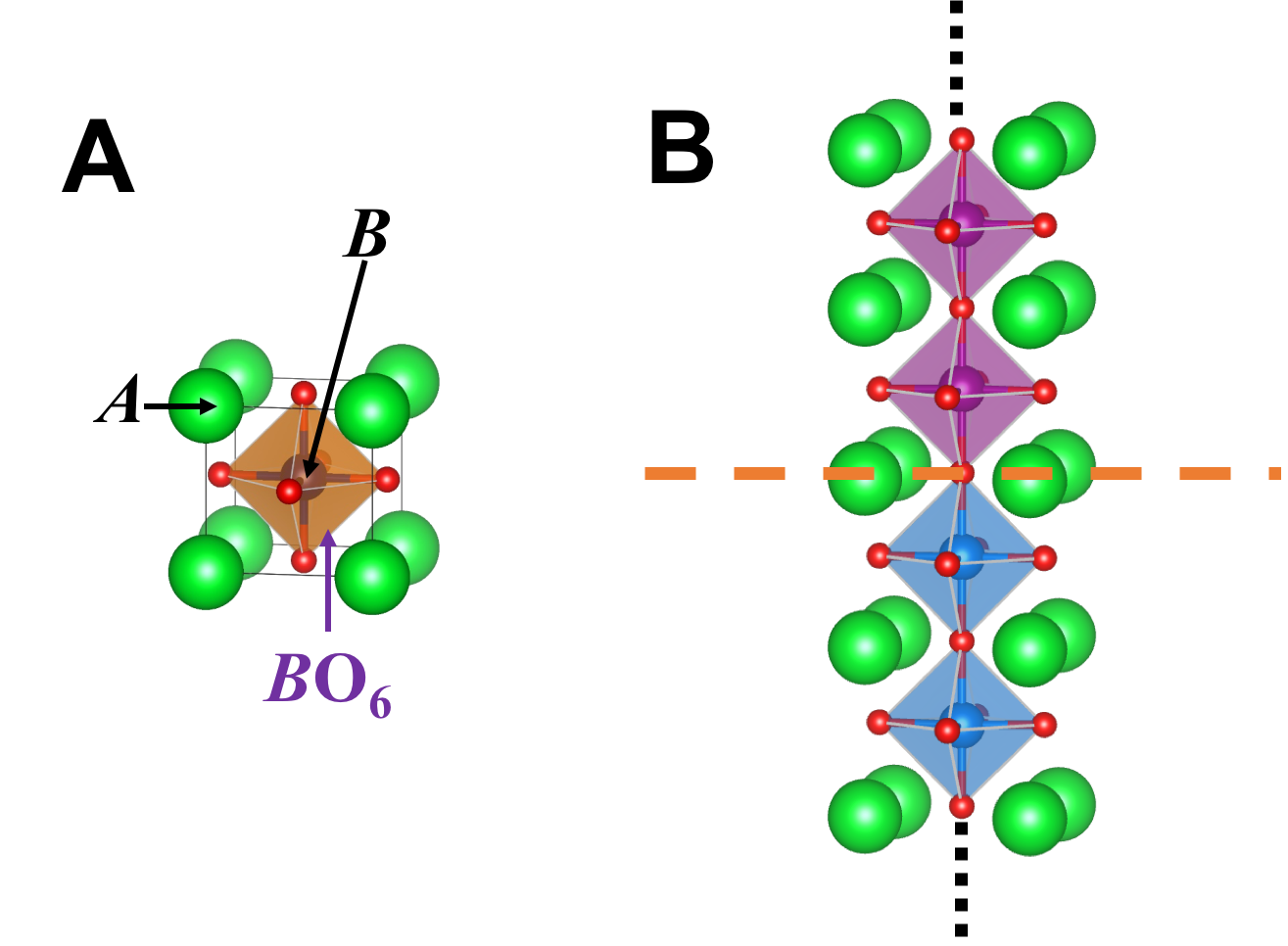
In this review we focus on an important class of transition metal oxides: perovskite oxides. Their atomic structure is shown in Fig. 1A. The atom on the corner of the cube is called -site atom, which is either an alkaline earth metal or a rare earth metal. The atom at the center of the cube is called -site atom, which is a transition metal. Each transition metal atom is surrounded by six oxygen atoms which are at face-center of the cube. As we form an oxide heterostructure using two perovskite oxides, we need to choose a stacking direction. In this review, unless otherwise specified, we focus on (001) interfaces, which are shown in Fig. 1B.
II Overview of charge-transfer mechanisms
The materials separated by an interface will generically have different electronic properties, and therefore different chemical potentials (measured, say, relative to the vacuum level) and this difference will generally lead to charge flow across the interface. With the transferred electrons, the physical and chemical properties of the constituent oxides close to the interface can be fundamentally different from bulk properties because the transition metal occupancy is changed.
In the context of oxide interfaces, it is useful to distinguish three driving mechanisms all of which contribute to the chemical potential difference: polarity difference, occupancy difference and electronegativity difference. The classification of different charge transfer mechanisms is not unambiguous. In fact, different mechanisms are closely related and sometimes intertwined. The classification is nonetheless useful, because charge transfer across oxide interfaces always occurs to compensate for some type of “discontinuity”, and our classification lists the three most relevant types.
II.1 Polarity difference
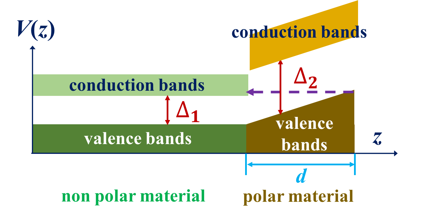
In this review, a polar material is understood as an insulator (polar metals have recently been experimentally synthesized Shi et al. (2013); Kim et al. (2016), which however goes beyond the scope of our current discussion) such that along a certain direction, in the form of a stoichiometric thin film, an average internal electric field develops. Correspondingly, a nonpolar material is an insulator such that in the stoichiometric thin film, along the given direction, the internal electric field is averaged to zero. For example, stoichiometric (001) LaAlO3 films are polar because they are composed of alternating (LaO)+1 and (AlO2)-1 layers, while stoichiometric (001) SrTiO3 films are nonpolar since they consist of alternating (SrO)0 and (TiO2)0 layers. However, we note that along the (110) direction, SrTiO3 can be considered as polar because of the alternating (SrTiO)4+ and (O2)4- layers.
We focus on [001] as the stacking direction. Fig. 2 illustrates the interface between a polar material and a nonpolar material. An average internal polar field is developed in the polar material along the [001] direction. The potential difference between one side of the polar material and the other side is proportional to the thickness of the material . Therefore as
| (1) |
electrons can tunnel from the surface to the interface ( is the band gap of the nonpolar material and is the band gap of the polar material). As a consequence of charge transfer, electrons emerge in the conduction band of the nonpolar material (if ) or in the conduction band of the polar material (if ) and holes appear in the valence band of the polar material (on the surface). The smallest value of that satisfies Eq. (1) defines the critical thickness. For the -type LaAlO3/SrTiO3 interface, the experimental critical thickness is 4 unit cells Thiel, S. Hammerl G, Schmehl A, Schneider CW (2006). As is above the critical thickness, the two-dimensional electron/hole gas at the interface and surface counteracts the internal field in the polar material. The sheet density of electrons/holes increases with the thickness of the polar material and approaches the saturation value as when the internal polar field is completely compensated Chen et al. (2010b); Millis and Schlom (2010); Mannhart et al. (2008).
However, we need to make two important comments:
1) we note that Eq. (1) is based on the assumption that valence bands are perfectly aligned. If there is a significant band misalignment between the polar and the nonpolar materials, Eq. (1) needs to be refined. However, the general picture that charge transfers from one side of the polar material to the other side above a critical thickness remains qualitatively the same.
2) the polar catastrophe mechanism provides one way to compensate the internal polar field. However, as the thickness of the polar material is large enough (in the limit of bulk materials), other compensation mechanism will be in play, such as vacancies, interstitials and adsorbed molecules. The thickness dependence of sheet carrier density only applies to the situation without defect formation.
II.2 Occupancy difference
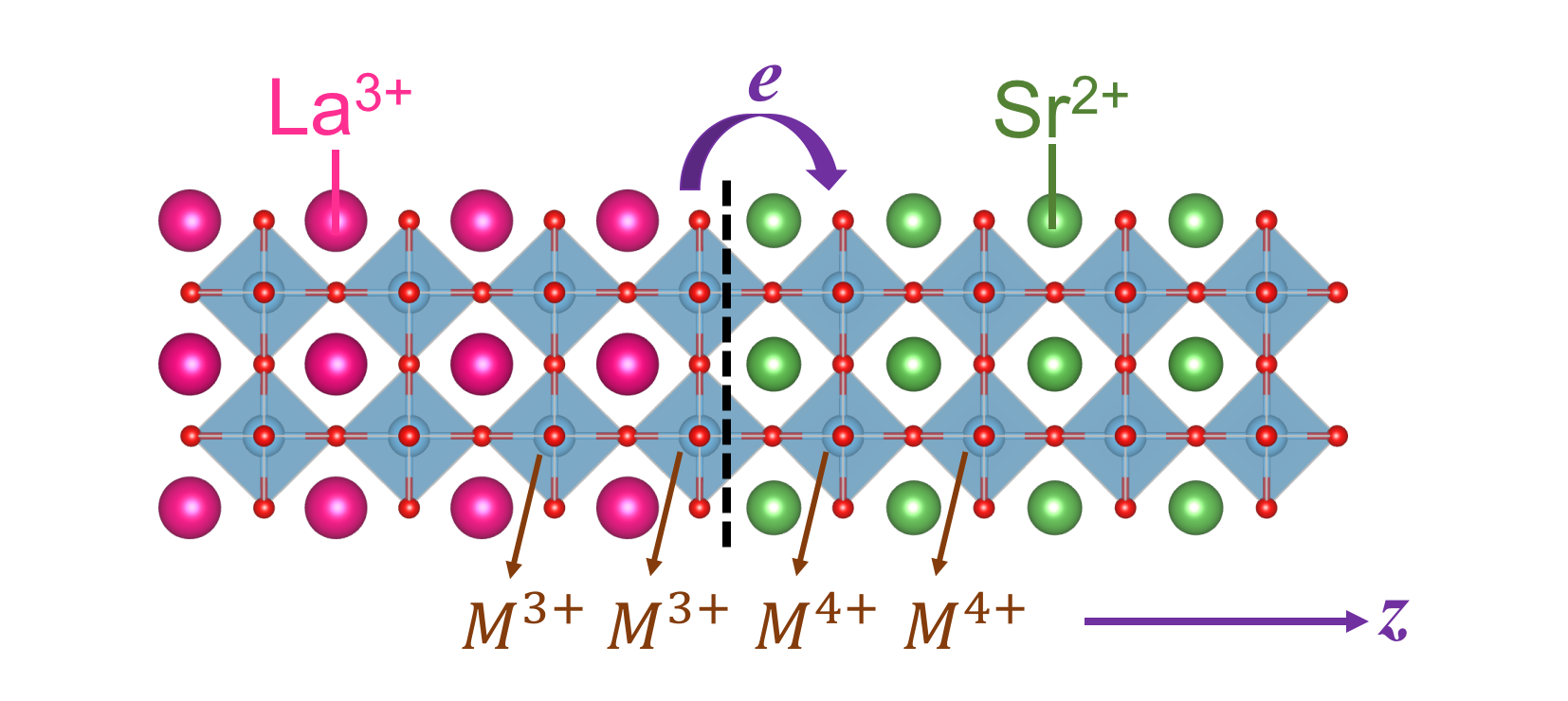
The second mechanism is the difference of transition metal occupancy across the interface. Many transition metal ions, such as Ti, V and Mn, have multiple valences and the valence state can be controlled by other elements in a compound. For example, in O3 perovskite materials, one may think of the O ions as having formal valence , while the ion may have formal valence (if =Sr, Ca, Ba, etc) or (if =La or other member of the lanthanide series), so charge neutrality fixes the valence of the -site transition metal ions as (if = Sr) or (if = La). While formal valence is an oversimplification of the true situation, it provides a useful description. Fig. 3 illustrates the interface between LaO3 and SrO3. Without charge transfer, the formal valence of transition metal ion abruptly changes from 3+ to 4+ at the interface. This discontinuity drives a charge flow, so that some electrons on ions may flow to ions, which smoothes out the occupancy discontinuity at the interface. However, we note that difference in transition metal occupancy does not always lead to charge transfer, or even if charge transfer does occur, conduction does not necessarily emerge at the interface. This is ascribed to the competition between correlation effects and kinetic energies. We will discuss it in more details in subsequent sections.
II.3 Electronegativity difference
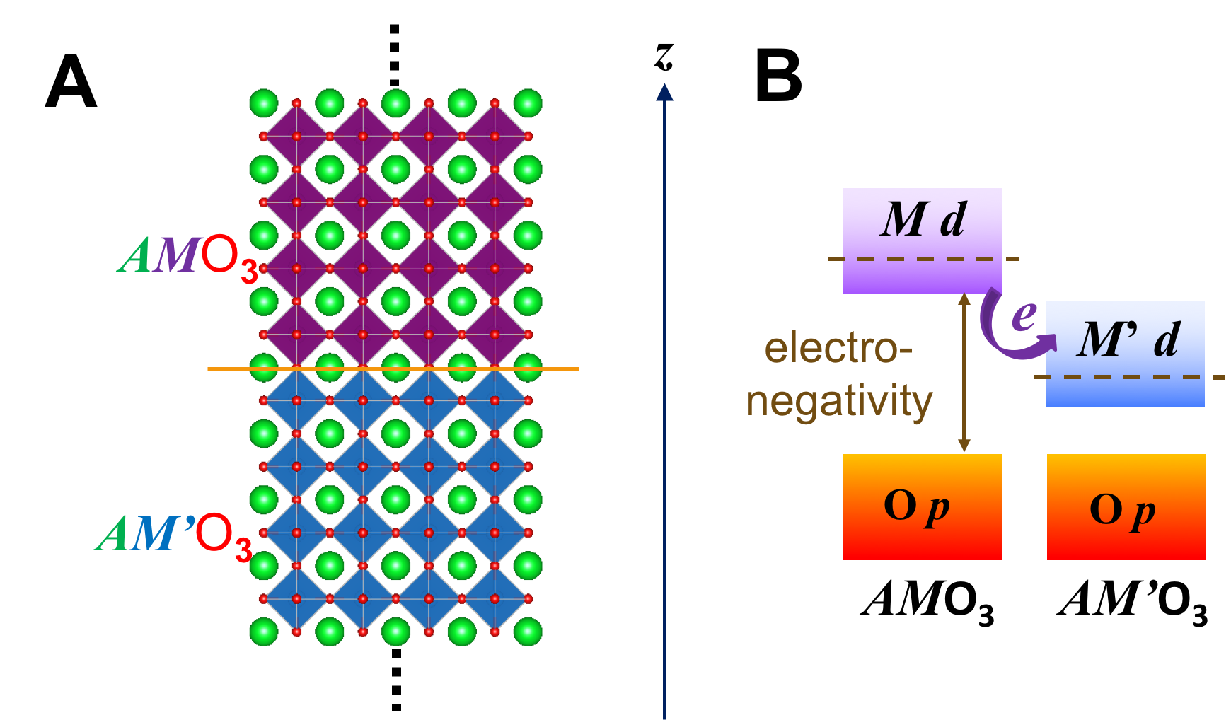
The third mechanism is the difference in electronegativity of dissimilar transition metal . Loosely speaking, electronegativity (or sometimes referred to as electron affinity) is a measure of the energy gain (or cost) of moving an electron from a reservoir to the ion in question; of course the value of the electronegativity depends on the choice of reservoir and on the valence of the ion. The electronegativity, defined at constant valence, decreases as one moves from left to right across the transition metal series and the differences in electronegativity play an important role in the magnitude of the charge transfer. As a rough rule of thumb, we observe that the greater the electronegativity difference, the greater the magnitude of the charge transfer. To make these considerations more specific and quantitative, we first remark that in transition metal oxides, one may think of the O2- as providing the reservoir. Thus the electronegativity is in essence the energy separation between transition metal and oxygen states, which is often referred to as the charge transfer energy Zaanen et al. (1985). In many oxide superlattices, the oxygen states approximately align across the interface so that the electronegativity difference translates directly into a contribution to the chemical potential difference and can drive charge transfer, as shown in Fig. 4A. This figure shows the interface between O3 and O3, where the two transition metal ions and have identical formal valences (i.e. no polar discontinuity), but have different energy levels of their states (different electronegativity) as shown in Fig. 4B, leading to transfer of electrons from to across the interface to reduce the total energy.
We note that similar to the previous discussion, we perfectly align the O states across the oxide interface in Fig. 4, which is an oversimplification: although the oxygen states form a continuous network the energies do not exactly align across interfaces. However, the simplified picture provides a very useful way of understanding the results of detailed calcuations.
III Polarity difference (Polar catastrophe)
The charge transfer mechanism of polarity difference at oxide interfaces is commonly known as the “polar catastrophe”. The term becomes commonly used after Ohtomo and Hwang synthesized LaAlO3 thin films of a few unit cells thick on SrTiO3 substrates with a TiO2 termination and discovered a high-mobility electron gas at the LaAlO3/SrTiO3 interface Ohtomo and Hwang (2004). While the LaAlO3/SrTiO3 interface (to be more precise, the one with LaO/TiO2 termination, sometimes referred to as the -type interface) is just one example of the “polar catastrophe” mechanism Nakagawa et al. (2006), it is an important special case which has stimulated numerous theoretical and experimental works, and led to many unexpected phenomena including magnetism Brinkman et al. (2007); Li et al. (2011); Bert et al. (2011), superconductivity Reyren et al. (2007); Caviglia et al. (2008) and tunable Rashba spin-orbital interaction Caviglia et al. (2010); Lesne et al. (2016). We refer readers to the excellent review papers that have already appeared in literature Huijben et al. (2009); Chen et al. (2010a); Pentcheva and Pickett (2010); Y (2012).
However, we want to comment that while the LaAlO3/SrTiO3 interface is the prototype of the“polar catastrophe” mechanism, accumulating evidence shows that the “polar catastrophe” mechanism alone can not explain all the observed experimental results. For example, early experiments failed to observe the average internal polar field in LaAlO3 Segal et al. (2009). Later experiments do report an internal polar field, but the magnitude is only 80 meV/Å Singh-Bhalla et al. (2011), smaller than the first-principles calculations by at least a factor of 2 Chen et al. (2009, 2010b). This implies that in addition to charge transfer, other mechanisms can also screen the internal polar field, leading to smaller values than theoretical predictions. Recently a polarity-induced defect mechanism was proposed to account for both conduction and magnetism at the LaAlO3/SrTiO3 interface Yu and Zunger (2014). Chambers et. al. Chambers et al. (2011) show that at the (100) LaCrO3/SrTiO3 interface, a potential gradient within the polar material LaCrO3 is sufficient to trigger a charge transfer, which one would expect to lead to conduction. However, the interface is experimentally found to be insulating. The insulating behavior was attributed to cation-intermixture.
All these results show that at a general polar-nonpolar interface, the “polar catastrophe” picture which is based on the ideal atomic structure probably is not the only mechanism in play. Atomic reconstruction, such as cation intermixture, various types of vacancies and point defects, are very likely to occur.
IV Occupancy difference
The charge transfer mechanism of occupancy difference between oxide interfaces are closely related to the “polar catastrophe” mechanism. However, we use this classification to refer to one particular type of superlattices which have been under intensive study. The general formula of those superlattices can be expressed as O3/O3 where is a tri-valent cation, is a di-valent cation and is a transition metal ion. The most common case for is La and for is Sr. Important examples of these oxide heterostructures include LaTiO3/SrTiO3 Ohtomo et al. (2002); Okamoto and Millis (2004), LaMnO3/SrMnO3 Monkman et al. (2012); May et al. (2009) and LaVO3/SrVO3 Lüders et al. (2009); Dang and Millis (2013a) superlattices.
Like the LaAlO3/SrTiO3 interface, there are also many reviews in literature discussing LaTiO3/SrTiO3, LaMnO3/SrMnO3 and related oxide heterostructures Pentcheva and Pickett (2010). Here we briefly review these important examples and mention some points that from our perspective deserve attention for future research.
Ref. Ohtomo et al. (2002) shows that as a few unit cells of Mott insulator LaTiO3 are embedded into a band insulator SrTiO3 matrix, electrons move from the Ti atoms in LaTiO3 to the Ti atoms in SrTiO3, providing emergent conduction at the interface. Similar phenomena have also been reported for a few unit cells of Mott insulating GdTiO3 embedded into an SrTiO3 matrix. The carrier concentration at this interface is even higher Moetakef et al. (2011a). Ref. Okamoto and Millis (2004) shows that charge transfer and conduction are general features at the interface between a semi-infinite Mott insulator and a semi-infinite band insulator. However, if we change the geometry, different phenomena can emerge. Refs. Jang et al. (2011) shows that if we insert only a single O layer in a SrTiO3 matrix, and if = La, Pr and Nd, conduction appears at the interface, but if = Sm and Y, the interface remains insulating. Ref. Moetakef et al. (2012); Chen et al. (2013a) study another related geometry: they consider inserting SrO in a Mott insulator GdTiO3 matrix and both theory and experiment find that due to extreme quantum confinement, a dimer Mott insulating state can be stabilized.
The second example is (LaMnO3)m/(SrMnO3)n superlattices with different Sr/La ratio (by varying and ). An important case is that , which deserves special attention Smadici et al. (2007). For (LaMnO3)2n/(SrMnO3)n superlattices, as increases from 1 to 5, a metal-insulator transition occurs (for , the interface is metallic and for , the interface becomes insulating) Bhattacharya et al. (2008). For the nature of insulating states, Ref. Bhattacharya et al. (2008) suggests that a finite peak does exist in the density of states at the Fermi level but it is localized by disorder. A recent experiment Monkman et al. (2012) proposes that it is the quantum fluctuation that disrupts the coherence of metallic states, giving rise to the insulating properties observed in superlattices. However, theoretical work Dong et al. (2008); Nanda and Satpathy (2009) shows that within a reasonable range of parameters, the ideal interface between semi-infinite LaMnO3 and semi-infinite SrMnO3 should be metallic.
In Ref. Lüders et al. (2009) the authors synthesize (LaVO3)m/(SrVO3)1 superlattices ( varies from 2 to 6) and find that the superlattices have a net magnetization up to room temperatures due to the geometrically confined doping. However, the authors of Ref. Dang and Millis (2013a, b) show theoretically that the experimentally determined crystal structure of LaVO3/SrVO3 superlattices is not favorable to induce ferromagnetism. They propose that large amplitude of oxygen octahedral rotations would be needed to stabilize a ferromagnetic state.
We note that for these (LaO3)m/(SrO3)n superlattices (where = Ti, Mn and V), their chemical composition is equivalent to La1-xSrO3 where and . The physical properties of solid solution La1-xSrO3 have also been comprehensively investigated in theory and experiment Imada (1998); Salamon and Jaime (2001). For or 1, the end material is usually insulating (band insulator or Mott insulator). In the solid solution (), conduction emerges within a range of . However, as we have seen from the above examples, with the same chemical composition, the superlattices can exhibit distinct properties from solid solutions. For examples, solid solution La2/3Sr1/3MnO3 is ferromagnetic metallic but (LaMnO3)10/(SrMnO3)5 superlattice is insulating. (LaVO3)6/(SrVO3)1 superlattice exhibits a large magnetic moment of 1.4 /V ion, whereas solid solution La6/7 Sr1/7VO3 shows a much smaller net magnetization. Another important difference of superlattices from compositionally equivalent solid solutions is the anisotropy of transport. While solid solutions usually show three dimensional conduction, the emergent conduction in superlattices is confined to interfaces and exhibits two dimensional character, which may be more useful for device development.
We also need to mention that in many systems, both charge occupancy difference and polarity effects will contribute to the charge transfer. The LaAlO3/SrTiO3 and LaTiO3/SrTiO3 Ohtomo et al. (2002), GdTiO3/SrTiO3 Moetakef et al. (2011b) systems provide useful examples. In the former, the Al valence is the same in all layers and the charge transfer depends strongly on the thickness of the polar LaAlO3 layers, becoming negligible for less than 4 unit cells, so here the charge transfer is entirely driven by polarization effects. In the latter systems the amount of charge transfer depends on the thickness of polar LaTiO3 (or GdTiO3) layers but does not vanish even for 1 monolayer. Furthermore, the near interface Ti ions in the LaTiO3 (or GdTiO3) have a valence different from that of the Ti farther from the interface; thus both mechanisms contribute in this system.
V Electronegativity difference
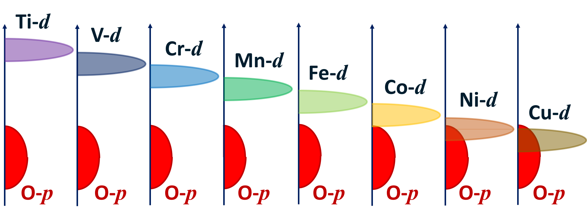
In this section, we present a detailed review of electronegativity-driven charge transfer in oxide heterostructures. We focus on the following interfaces O3/O3 or double perovskite O6, where is di-valent or tri-valent ion and , are dissimilar transition metal ions. Fig. 5 schematically shows the energy separation between metal and oxygen states for transition metal oxides LaO3 ( = Ti, V, Cr, Mn, Fe, Co, Ni and Cu). We note that as the mass of transition metal element increases, the Coulomb attraction to the nucleus lowers the energy of transition metal states, so the electronegativity increases as one move from left to right along the transition metal row. For titanates, the energy separation between Ti- and O- states is about 3 eV. However, for nickelates and cuprates, the Ni- and Cu- states lie even below the O- states, which leads to a “negative charge transfer” energy and strong hybridization between metal and oxygen states. The electronegativity-driven charge transfer is based on the energy difference between the states of two different transition metal ions.
Before we move on, we note that an electronegativity difference does not always drive charge transfer. If one material O3 is a wide gap insulator with a nominally empty - shell and the states of ions lie above those of ions, then no charge transfer occurs between and ions. SrTiO3/SrVO3 is one example in which there is no charge transfer between SrTiO3 and SrVO3 Yoshimatsu et al. (2010). LaAlO3/LaNiO3 is another example Boris et al. (2011). This situation is called quantum confinement which reduces the band width of transition metal ions and also leads to emergent phenomena, but it goes beyond the scope of our current paper and we refer the readers to other review papers Stemmer and Millis (2013).
V.1 LaTiO3/LaNiO3 and LaTiO3/LaNiO3/insulator superlattices
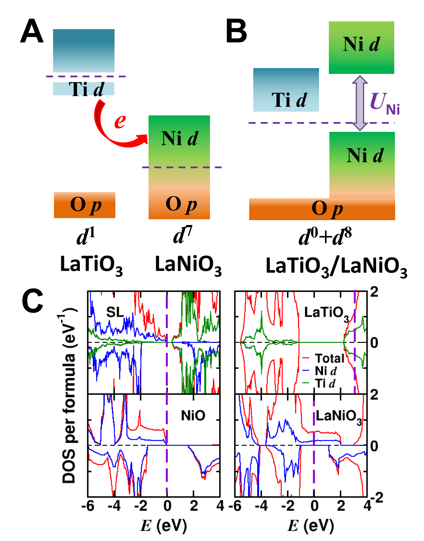
We start from the interface between LaTiO3 and LaNiO3. Bulk LaTiO3 is an antiferromagnetic Mott insulator with a nominal occupancy on Ti atoms. Bulk LaNiO3 is a paramagnetic metal with a nominal occupancy on Ni atoms. As Fig. 6A shows, in bulk LaTiO3, Ti- states lie above O- states by about 3 eV, while in bulk LaNiO3, Ni- states have strong hybridization with O- states. In a LaTiO3/LaNiO3 superlattice with a short periodicity, the lone electron on Ti- states is expected to transfer to Ni- states. Therefore after the charge transfer, in the superlattice Ti atoms nominally have a occupancy and Ni atoms nominally have a occupancy. In the new charge configuration, as Fig. 6B shows, Ti atoms have an empty shell. Ni atoms have a full shell and a half-filled shell. If the correlation strength on Ni sites is strong enough, a Mott gap will open up. In this way, by design, we can induce an artificial Mott insulating state via a nominally complete charge transfer from Ti to Ni in LaTiO3/LaNiO3 superlattices Chen et al. (2013b). Fig. 6C presents the theoretically calculated density of states for (LaTiO3)1/(LaNiO3)1 superlattices, as compared to the density of states for the classical Mott insulator NiO (in which Ni atoms also nominally have a occupancy) as well as bulk LaNiO3 and LaTiO3. We can see that the Ti- conduction bands, which are partially filled in bulk LaTiO3, become completely empty in the (LaTiO3)1/(LaNiO3)1 superlattice. On the other hand, the Ni- states, which are partially filled in bulk LaNiO3, are filled up in the (LaTiO3)1/(LaNiO3)1 superlattice. As a consequence, a gap is opened in the superlattice, which separates Ni- and Ti- states. The lower and upper Hubbard bands of Ni- states in the superlattice are very similar to those in NiO, which is a strong evidence of the charge-transfer-driven Mott insulating state on Ni sites.
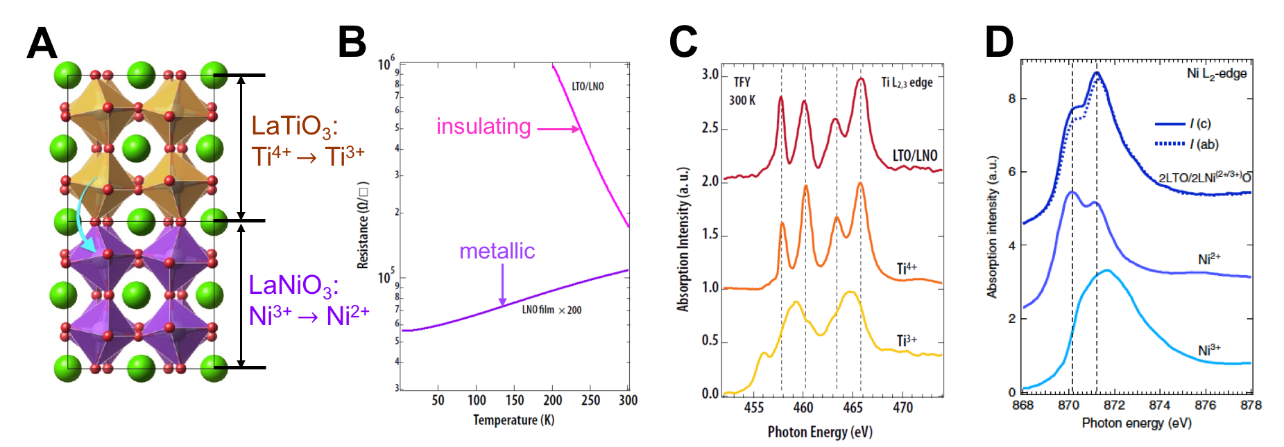
Inspired by the theoretical predictions in Ref. Chen et al. (2013b), Cao et al. Cao et al. (2016) synthesized a (LaTiO3)2/(LaNiO3)2 superlattice and measured the transport properties. Fig. 7A shows the atomic structure of the superlattice. Fig. 7B shows the temperature dependence of sheet resistance of (LaTiO3)2/(LaNiO3)2 superlattice and LaNiO3 film. The former is highly insulating while the latter exhibits metallic behavior. To probe the change in charge states, Fig. 7C and D show the Ti and Ni edge of (LaTiO3)2/(LaNiO3)2 superlattices measured by the x-ray absorption spectroscopy. Panel C shows that the formal valence of Ti in the superlattice changes from the value 3+ in bulk LaTiO3 to 4+ as in SrTiO3, while the formal valence of Ni in the superlattice changes from the value 3+ in bulk LaNiO3 to 2+ as in NiO. These results are consistent with the theoretical predictions in Ref. Chen et al. (2013b) and provide convincing evidence of charge transfer in the (LaTiO3)2/(LaNiO3)2 superlattices.
In addition to the charge transfer from Ti to Ni across the interface between titanates and nickelates, Grisolia et. al. Grisolia et al. (2016) find a more subtle effect. By synthesizing and comparing GdTiO3/NiO3 interfaces ( = La, Nd, Sm), they find that the magnitude of charge transfer from Ti to Ni can be tuned by the element . The charge transfer increases from LaNiO3 to NdNiO3 to SmNiO3. The underlying mechanism is that different ionic sizes of affect the oxygen octahedral rotations and thus hybridization between Ni- and O- states. Because what we for simplicity refer to as the -state is an antibonding - hybrid, the - covalency affects the energy. Therefore, in addition to the energy gain by moving electrons from Ti- states of higher energies to Ni- states of lower energies, Ni- and O- states change their hybridization and covalent character (so-called “rehybridization”), which also costs energy. The larger the ionic size, the more energy the rehybridization costs, which limits the amount of charge that can be transferred across the interface. It is noteworthy Grisolia et al. (2016) that while hybridization in NiO3 tunes the charge transfer from Ti to Ni across the interface between GdTiO3 and NiO3, hybridization in TiO3 plays a much less significant effect on the charge transfer across the interface between TiO3 and LaNiO3. The reason is that different from strong hybridization between Ni- and O- states, in titanates Ti- states lie above O- states by about 3 eV, which results in a much weaker hybridization between Ti- and O- states. Therefore, changing the ionic size of in TiO3 can not significantly tune the hybridization and therefore does not have the controlling effects on charge transfer as eminent as it does in NiO3.
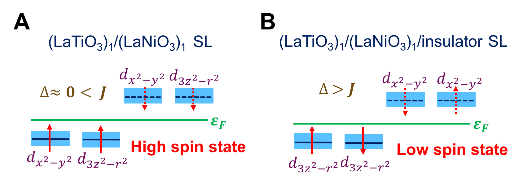
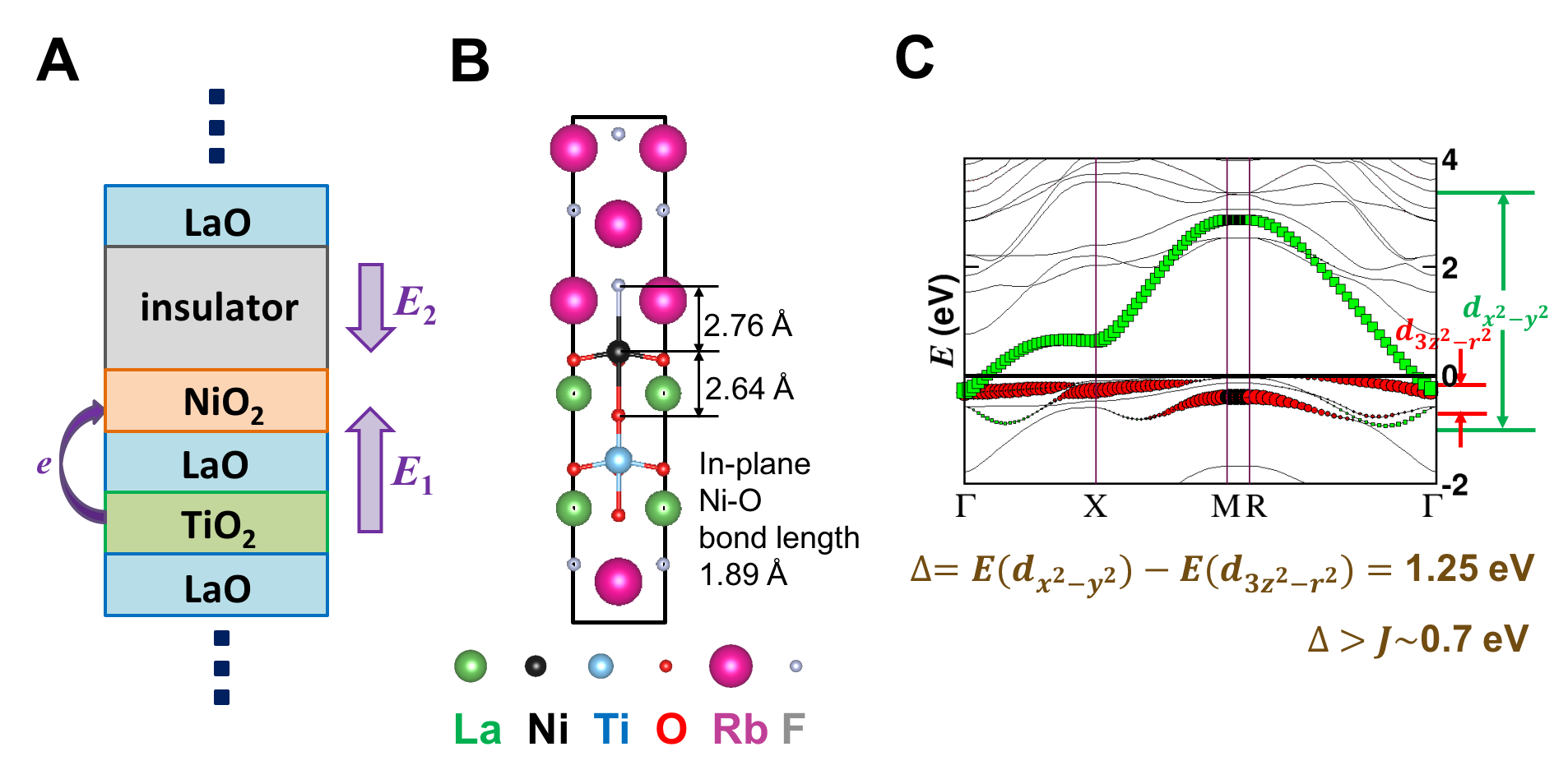
Next we discuss a LaTiO3/LaNiO3/insulator tri-component superlattice Chen et al. (2013c). The motivation of designing such a new superlattice is to engineer an unprecedented orbital state in Ni atoms (in addition to the change in charge states) Chaloupka and Khaliullin (2008); Hansmann et al. (2009). As in the LaTiO3/LaNiO3 superlattice, nominally one electron transfers from Ti to Ni in the tri-color superlattice, which leads to a Ni occupancy with a full shell and two electrons in the shell. However, they have fundamental difference. As Fig. 8 shows, in the LaTiO3/LaNiO3 superlattice, the two electrons in the Ni shell form a high-spin state, while in the tri-component superlattice, the two electron in the Ni shell form a low-spin state. The high-spin/low-spin configuration is determined by the competition between Hund’s coupling and crystal field splitting , which is the energy difference between Ni and orbitals. If , the two electrons fill two different orbitals with the same spin, leading to a high-spin state. If , the two electrons fill the same orbital with opposite spins, leading to a low-spin state. The significance of a low-spin state in Ni-based oxide heterostructures is that further electron doping of the tri-component superlattice can induce a single-orbital Fermi surface, analogous to that of superconducting cuprates.
The orbital splitting between and orbitals is induced by a Jahn-Teller-like distortion, i.e. elongation of out-of-plane Ni-O bonds. Such a structural distortion occurs to the tri-component superlattice by the combination of charge transfer and insertion of a wide-gap insulator. Fig. 9A shows the schematics of a (LaTiO3)1/(LaNiO3)1/insulator tri-component superlattice. Charge transfer from Ti to Ni induces an internal electric field and due to the periodic boundary condition a second electric field appears. Both and pull the apical oxygen atoms away from the Ni atom, which leads to Jahn-Teller-like distortions that favor the occupancy of Ni orbital over the orbital. The presence of a wide gap insulator explicitly breaks the inversion-symmetry and leads to . This asymmetry induces a polar distortion on Ni atoms, i.e. Ni and O are not co-planar, which further increases the out-of-plane Ni-O bond length. Fig. 9B shows the theoretically calculated atomic structure of (LaTiO3)1/(LaNiO3)1/(RbF)3 superlattices. We note that the out-of-plane Ni-O and Ni-F bond lengths are on average equal to 2.7 Å, which is much longer than the in-plane Ni-O bond length 1.89 Å. The ferroelectric-like Ni-O displacement is clearly visible. Fig. 9C shows the band structure of (LaTiO3)1/(LaNiO3)1/(RbF)3 superlattice. The red symbols are band projections onto Ni orbital. The green symbols are band projections onto Ni orbital. The Ni band is almost completely filled up while the Ni band is nearly empty. This confirms that the tri-component superlattice indeed has a low-spin configuration (two electrons fill the same orbital with opposite spins). On the other hand, using the maximally localized Wannier functions and fitting them to the DFT-calculated band structure, the difference between the onsite energy for Ni orbital and that for Ni orbital is calculated to be 1.25 eV. The Hund’s coupling for Ni orbital is about 0.7 eV. Therefore it is , which is consistent with the low-spin configuration.
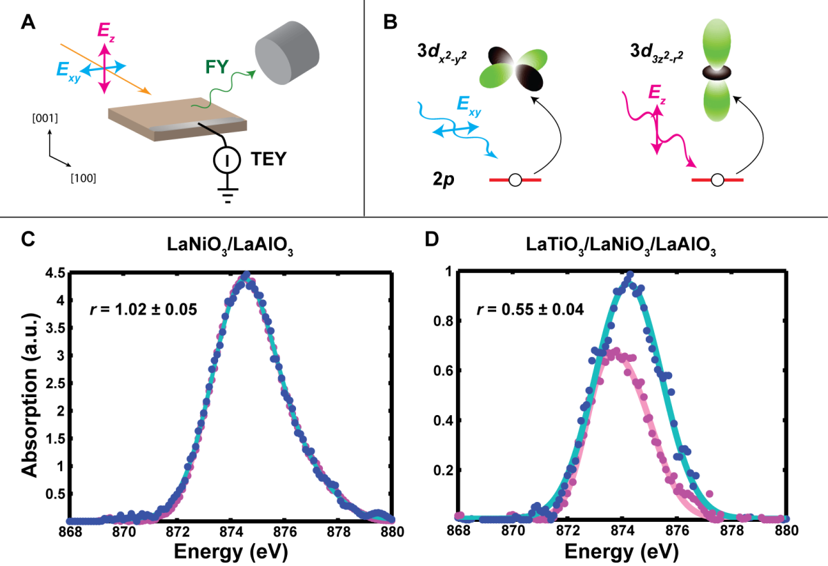
Following the theoretical proposal of Ref. Chen et al. (2013c), Disa et al. Disa et al. (2015) synthesized an artificial (LaTiO3)1/(LaNiO3)1/(LaAlO3)3 superlattice and used x-ray linear dichroism (XLD) to probe the orbital occupancy. Fig. 10A shows the experimental setup and Fig. 10B shows the orbital selective atomic transitions probed by the x-rays. The experiments compared LaNiO3/LaAlO3 superlattice (two-component superlattice) and the tri-component superlattice. The resulting orbital-polarization-dependent spectra are shown in Fig. 10C and D. In the two-component superlattice, no significant dichroic signal is observed (panel C). The red (absorption for Ni orbital) and blue (absorption for Ni orbital) symbols almost overlap with each other. In contrast, there is a marked dichroism for the tri-component superlattice (panel D). This result represents the largest experimentally observed Ni orbital polarization in perovskite nickelate systems to date. Furthermore, the Ni orbital occupancy measured experimentally is in good agreement with first-principles DFT calculations. However, G. Fabbris et al. Fabbris et al. (2016) measured resonant inelastic x-ray scattering (RIXS) spectra for this superlattice recently and obtained good fits to the spectra by using a -only model, i.e. we consider excitations from a Ni atom without explicitly including oxygen states. The fits give an on-site energy splitting between the two Ni orbital of only about 0.2 eV in the superlattice, whereas a -only Wannier function analysis of the DFT-calculated band structure gives an on-site splitting of about 0.8 eV Disa et al. (2015). This discrepancy, along with the fact that the -only RIXS does yield the predicted orbital polarization, has been attributed to the hybridization between Ni and O states Fabbris et al. (2016). We believe that the -only Wannier functions which are used to fit the DFT band structure treat - hybridization in a different manner from the -only RIXS model. Nevertheless, both the DFT calculations and the experimental spectra (XLD and RIXS) find a large orbital polarization in the (LaTiO3)1/(LaNiO3)1/(LaAlO3)3 superlattice. Further work is needed to address these remaining issues.
V.2 LaTiO3/LaFeO3 and YTiO3/YFeO3 superlattices
LaTiO3/LaFeO3 and YTiO3/YFeO3 superlattices are another example of a nominally complete charge transfer from Ti to Fe. The two superlattices share similarities but also have important differences.
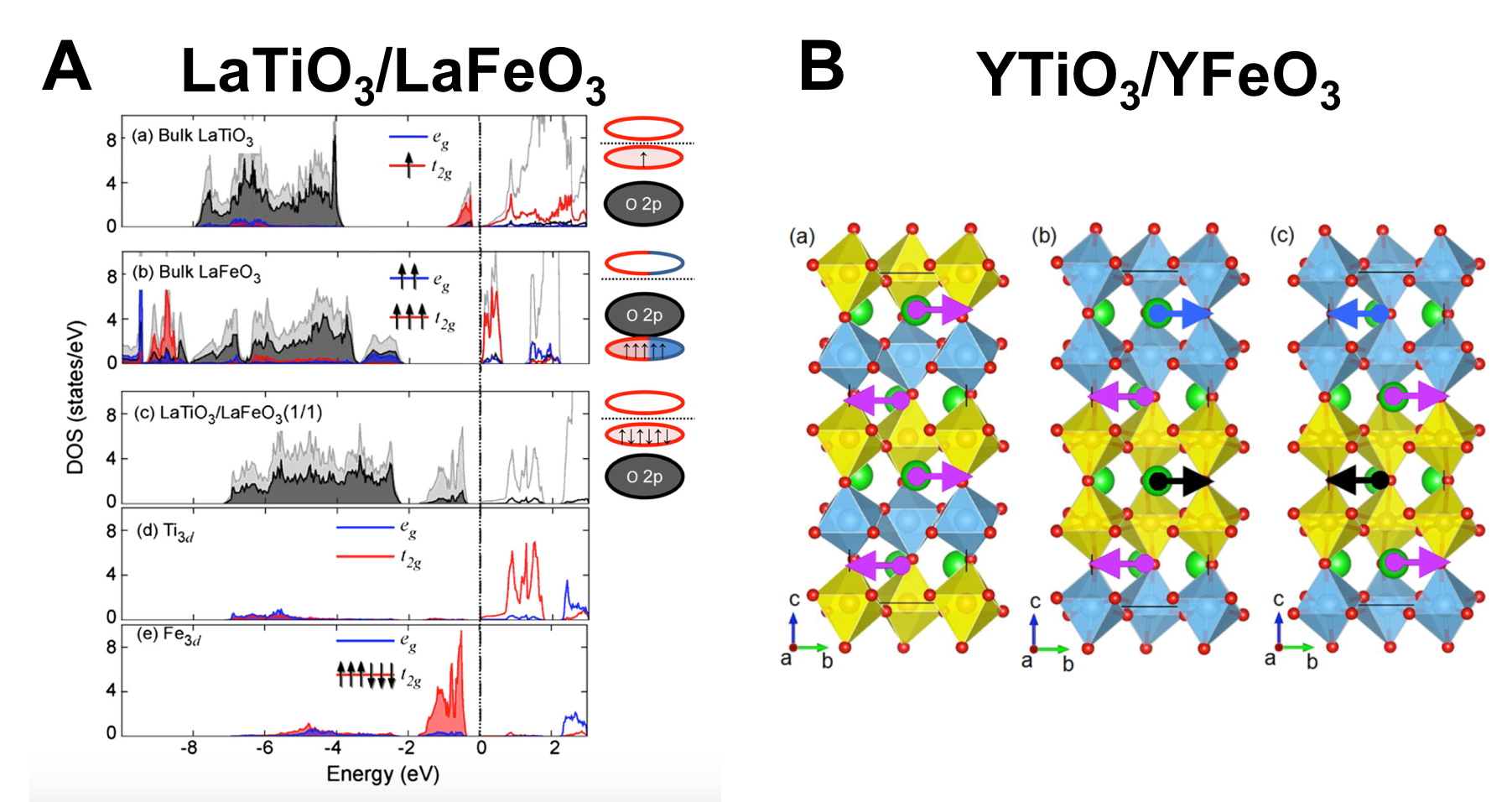
Bulk LaFeO3 (YFeO3) nominally has a Fe occupancy. The half-filled Fe shell forms a high-spin state. Bulk LaTiO3 (YTiO3) nominally has a Ti occupancy. Ref. Kleibeuker et al. (2014) shows both in theory and in experiment that Ti atoms nominally donate one electron to Fe atoms across the LaTiO3/LaFeO3 interface and after the charge transfer Fe atoms nominally have a occupancy but a high-spin to low-spin transition occurs and the six electrons completely fill the Fe shell. Fig. 11A illustrates such a charge-transfer-driven spin transition. The theoretically calculated density of states shows an empty Ti shell and a fully occupied Fe shell. Experimentally, by using x-ray photoelectron spectroscopy, the authors of Ref. Kleibeuker et al. (2014) confirmed the rearrangement of the Fe bands and revealed an unprecedented charge transfer up to per interface unit cell in the LaTiO3/LaFeO3 heterostructures. In YTiO3/YFeO3 superlattices, a similar charge transfer from Ti to Fe is also found in theory Zhang et al. (2015). However, in contrast to the LaTiO3/LaFeO3 superlattices, a robust high-spin state is found in the YTiO3/YFeO3 superlattices, probably due to the small ionic size of Y which leads to a smaller bandwidth of Fe states and favors the high-spin configuration. In addition to the high-spin state, hybrid ferroelectricity with a polarization C/cm2 is induced in a (YTiO3)2/(YFeO3)2 superlattice. Fig. 11B shows the atomic structure of (YTiO3)n/(YFeO3)n superlattices (=1 and 2) with arrow highlighting the displacement of Y atoms. If , all the Y atoms have the same environment. If , there are three types of Y atoms: one is sandwiched between TiO6 and FeO6, one is sandwiched between two TiO6 and one is sandwiched between two FeO6. The displacements of all three types of Y atoms do not exactly cancel each other, which leads to a net polarization.
We note that in Ref. Kleibeuker et al. (2014); Zhong and Hansmann (2016), the authors align the valence band edge of O- and find the occupied Ti states have overlap with the empty upper Hubbard bands of Fe- states in the energy window. However, in Ref. Zhang et al. (2015), the authors align the localized O- states and find the occupied Ti- states lie between the occupied lower Hubbard bands and the unoccupied upper Hubbard bands of Fe- states. However, in the calculations of both superlattices, charge transfer occurs from Ti to Fe atoms. This shows that the rigid band alignment using the bulk band structures can only serve as an approximate guide. Charge transfer and the resulting band alignment at oxide interfaces should be determined in a self-consistent way, as performed in superlattice calculations.
V.3 LaMnO3/LaNiO3 superlattices
Next we discuss the LaMnO3/LaNiO3 superlattice. This is an interesting case, since up till now there is inconsistency between theory and experiment. While both theory and experiment indicate that charge transfer from Mn to Ni occurs due to electronegativity differences, experimental transport and optical measurements show that (LaMnO3)2/(LaNiO3)2 superlattices are insulating Hoffman et al. (2013); Di Pietro et al. (2015) but theoretical calculations find that the (LaMnO3)m/(LaNiO3)n superlattices with different Mn/Ni ratios are all metallic Lee and Han (2013).
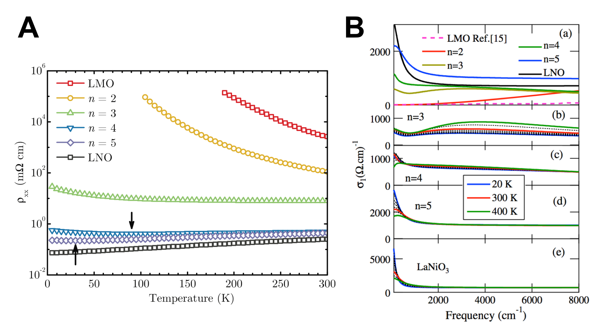
Fig. 12A shows the transport properties of (LaMnO3)2/(LaNiO3)n superlattices. As decreases from 5 to 2, a metal-insulator transition occurs. In particular, in experiment the (LaMnO3)2/(LaNiO3)2 superlattice exhibits strong insulating behavior. Fig. 12B shows the optical conductivity of (LaMnO3)2/(LaNiO3)n as a function of , temperature and frequency. Similar to transport measurements, the low frequency optical conductivity substantially drops as decreases from 5 to 2. In both Ref. Hoffman et al. (2013) and Ref. Di Pietro et al. (2015), the authors ascribe the observed metal-insulator transition to the charge transfer from Mn to Ni. Such a charge transfer in confirmed in first-principles calculations Lee and Han (2013). However, for both (LaMnO3)1/(LaNiO3)1 and (LaMnO3)2/(LaNiO3)2, no insulating state is stabilized in the calculations. Tuning the Hubbard for Mn and Ni orbitals in a reasonable range does not change the metallic properties of the superlattice. This raises the question whether the charge transfer from Mn to Ni is a nominally complete charge transfer or not. If it is, then presumably a Mott insulating state should emerge in (LaMnO3)1/(LaNiO3)1 superlattice where Mn atoms have a half-filled shell and Ni atoms have a full and half-filled shell, similar to (LaTiO3)1/(LaNiO3)1 superlattice. However, theoretical calculations show that a partial charge transfer from Mn to Ni occurs and the superlattice remains metallic. We note that double perovskite La2MnNiO6 is found to be a ferromagnetic insulator in both theory Das et al. (2008) and experiment Singh et al. (2007, 2009). The inconsistency between theory and experiment on LaMnO3/LaNiO3 superlattices implies that the interface may not be atomically sharp and disorder such as antisite defects Chen and Millis (2016) could play a role in inducing the insulating state. Further research, in particular characterization of interfacial atomic structure using high-resolution electron microscopy, may help to resolve the problem.
We note here that for LaMnO3/LaNiO3 interfaces, in addition to (001) stacking direction, (111) interfaces have also been synthesized and studied Gibert et al. (2012, 2016). Ref. Gibert et al. (2012) shows that at (111) LaMnO3/LaNiO3 interface, in addition to charge transfer, exchange bias emerges, which implies the development of interface-induced magnetism in the paramagnetic LaNiO3 layers. Such a bias does not show up at the (001) LaMnO3/LaNiO3 interface.
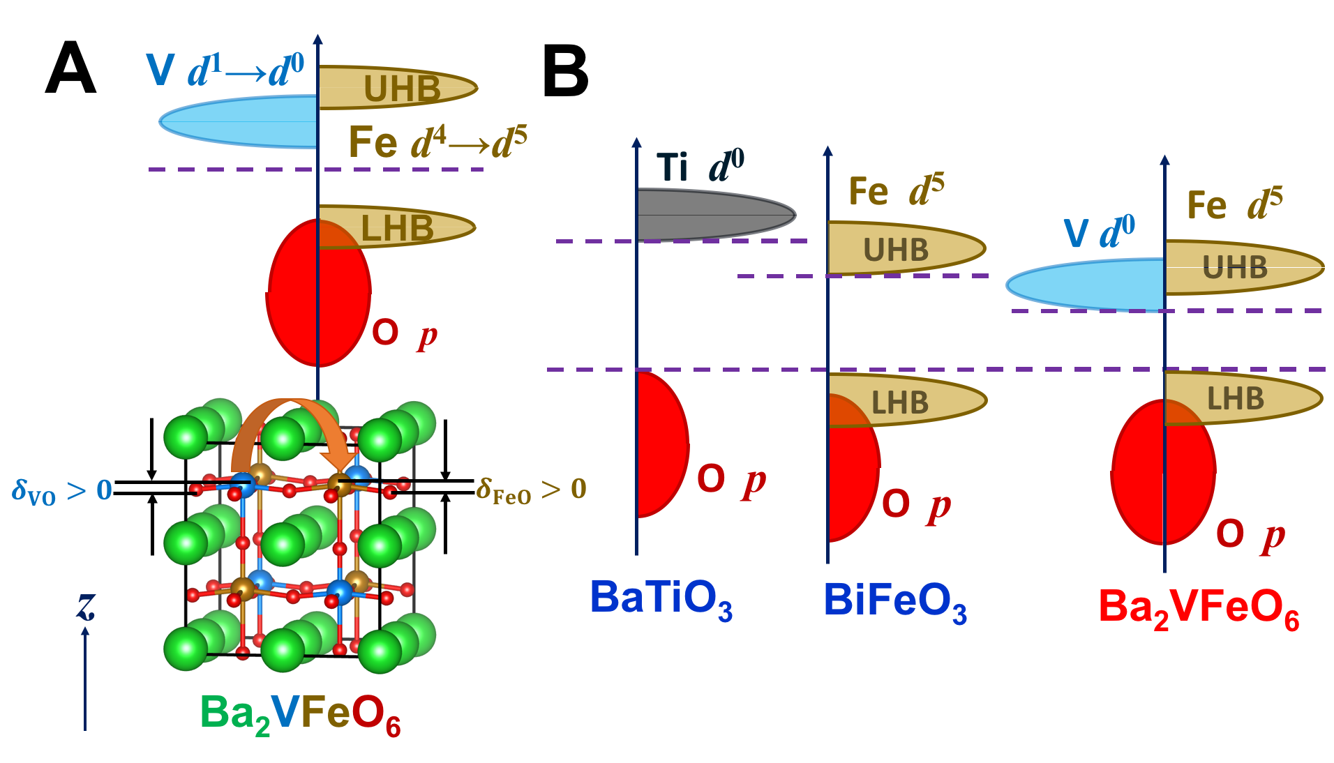
V.4 Ba2VFeO6, Pb2VFeO6 and Sr2VFeO6 double perovskite oxides
Substantial charge transfer not only occurs to atomically sharp interfaces in superlattices, but also in double perovskite which are bulk compounds that are based on two single perovskite oxides (see Fig. 13 for the atomic structure). Double perovskite Ba2VFeO6 is one example in which a nominally complete transfer from V to Fe leads to Mott multiferroic properties which do not exhibit in either bulk BaVO3 or bulk BaFeO3. Perovskite BaVO3 crystallizes in cubic structure with a nominally V occupancy. Perovskite BaFeO3 also crystallizes in cubic structure with a nominally Fe occupancy. As Fig. 13A shows, in the double perovskite Ba2VFeO6, a nominally complete charge transfer leads to new charge configurations V and Fe . Since Fe atoms have a half-filled configuration, strong correlation is expected to open a Mott gap. At sufficiently low temperatures, the large local magnetic moment on Fe atoms is expected to order magnetically. More importantly, both the empty V shell and the half-filled Fe shell have a ferroelectric instability, just like the Ti state in BaTiO3 and the Fe state in BiFeO3. The presence of Ba ions which have a large ionic size creates favorable conditions for ferroelectricity Wu et al. (2011). Fig. 13B compares the band structure of BaTiO3, BiFeO3 and Ba2VFeO6. In BaTiO3 and Ba2VFeO6, both Ti and V have occupancy. However, due to the electronegativity difference between Ti and V, the Ti states lie above the V states, which leads to a smaller band gap for Ba2VFeO6 than for BaTiO3. On the other hand, in both BiFeO3 and Ba2VFeO6, the Fe atoms have a state. However, in Ba2VFeO6, we have an empty V shell. Injecting one electron on V atoms changes its occupancy from to , which does not involve correlation effects. Injecting one electron on Fe atoms changes its occupancy from to , which increases the number of electron pairs and each additional pair is associated with a Hubbard energy. Therefore the V state is expected to lie below the upper Hubbard band of Fe state, which means a smaller gap for Ba2VFeO6 than for BiFeO3.
Ref. Chen and Millis (2017) uses first-principles calculations to support the above picture. In particular, the authors find that the polarization of Ba2VFeO6 is comparable to that of BaTiO3 and the gap of Ba2VFeO6 is smaller than that of BaTiO3 by about 1 eV. Since the experimental optical gap of BaTiO3 is 3.2 eV, it is predicted that the optical gap of Ba2VFeO6 is around 2.2 eV, which is 0.5 eV smaller than the optical gap of BiFeO3. This makes Ba2VFeO6 a promising candidate among perovskite oxides for bulk photovoltaic applications.
In addition to Ba2VFeO3, double perovskite Pb2VFeO6 has a ferroelectric polarization comparable to PbTiO3. Double perovskite Sr2VFeO6, like SrTiO3, is paraelectric but in the vicinity of ferroelectric-paraelectric phase boundary. We note that in terms of ferroelectric properties, VFeO6 has a simple one-to-one correspondence to TiO3 (=Ba, Pb, Sr).
V.5 SrVO3/SrMnO3 and Sr2VO4/Sr2MnO4 superlattices
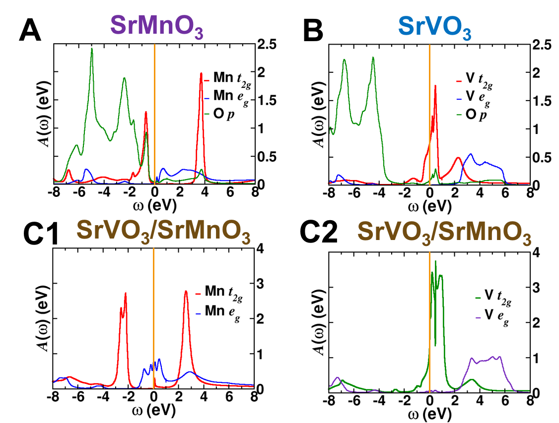
In addition to the cases of nominally “complete” charge transfer (the formal valence of cation ion changes by ) that are reviewed above, we may also have partial charge transfer, if the electronegativity difference between two similar transition metals is moderate. Partial charge transfer generically leads to emergent metallic properties due to the non-integer filling of bands. Ref. Chen et al. (2014) studies SrVO3/SrMnO3 superlattices. Bulk SrVO3 is a paramagnetic metal with a nominal V occupancy, while bulk SrMnO3 is an antiferromagnetic insulator with a nominal Mn occupancy. In the SrVO3/SrMnO3 superlattice, the partially occupied V states have similar energy to the empty Mn states, which results in an incomplete charge transfer, i.e. nominally the valence of V changes from 4 to and the valence of Mn changes from 4 to where . Fig. 14 shows the theoretically calculated spectral functions of bulk SrMnO3, SrVO3 and (SrMnO3)1/(SrVO3)1 superlattice. All the calculations are performed in paramagnetic states. Fig. 14A shows that a Mott gap is opened in bulk SrMnO3. Fig. 14B shows that bulk SrVO3 is paramagnetic metallic with V states at the Fermi surface. The panels C of Fig. 14 show the spectral function of (SrMnO3)1/(SrVO3)1 superlattice. In Fig. 14C1, the Mn states are partially occupied, which leads to emergent metallic behavior on Mn atoms in the superlattice. In Fig. 14C2, the V states are still partially occupied instead of empty, indicating that nominally less than one complete electron is transferred from V to Mn, in contrast to the complete charge transfer in (LaTiO3)1/(LaNiO3)1 superlattice. Furthermore, since SrMnO3 is electron doped, the double exchange mechanism favors a ferromagnetic ordering, just as in La1-xSrxMnO3 Salamon and Jaime (2001). In the (SrVO3)1/(SrMnO3)1 superlattice, ferromagnetism is expected to emerge in the MnO2 layer.
A closely related oxide heterostructure is Sr2VO4/Sr2MnO4 superlattice Chen et al. (2014). In this 214 Ruddlesden-Popper superlattice, similar charge transfer phenomenon from V to Mn occurs like the counterpart SrVO3/SrMnO3 superlattice. Synthesizing transition metal oxides of a complicated Ruddlesden-Popper structure is now feasible in experiment Lee et al. (2013). Designing Ruddlesden-Popper superlattices is an interesting direction for future research.
V.6 manganite/cuprate interfaces
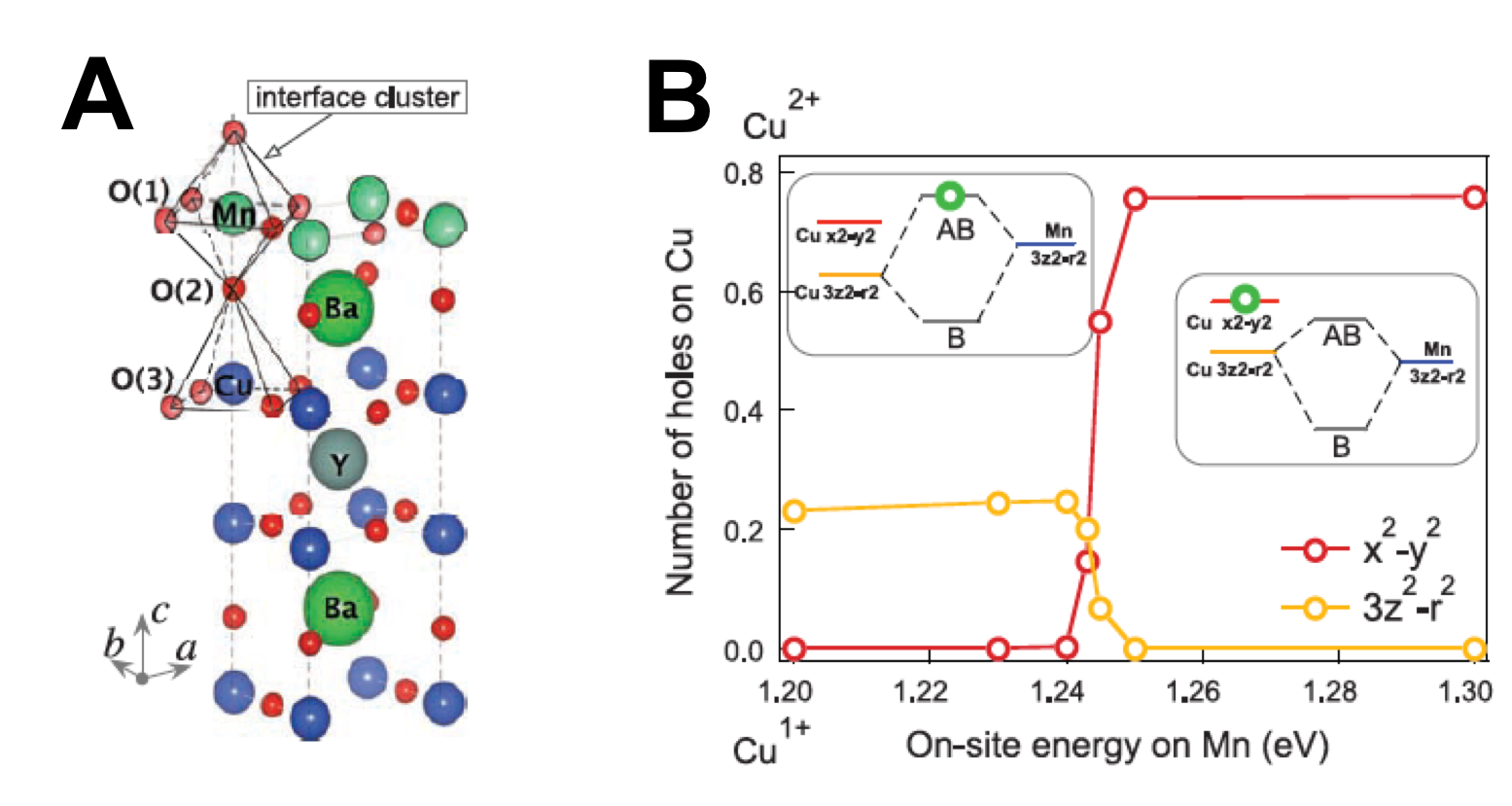
Partial charge transfer also occurs to the interface between the ferromagnetic conducting manganite La2/3Ca1/3MnO3 and the superconducting cuprate YBa2Cu3O7. The atomic structure of the interface is shown in Fig. 15A. It is more complicated than the O3/O3 superlattices, but the underlying charge transfer can be understood in a similar way to the previous examples we have reviewed.
In Ref. Chakhalian et al. (2007), the authors observe a 0.2 charge transfer from Mn to Cu per ion pair across the interface between La2/3Ca1/3MnO3 and YBa2Cu3O7. The direction of charge transfer can be deduced from our simple schematics of Fig. 5 that with respect to O- states, Mn- state lie above Cu- states. Fig. 15B shows a detailed analysis of charge transfer at the interface. In theory, the on-site energy on Mn can be considered as a tuning parameter to control the charge transfer. In the right inset of Fig. 15B, the energy of Mn has the same energy as that of Cu and the hole resides on Cu orbital. In the left inset of Fig. 15A, as the energy of Mn increases, a partial charge transfer occurs from Mn to Cu. In addition, the antibonding state formed by Cu and Mn orbitals has higher energy than that of Cu orbital. Therefore the hole on Cu atoms moves from to orbitals. In Ref. Chakhalian et al. (2006), at the same interface, the authors also find significant re-arrangement of magnetic domain structures accompanying charge transfer from Mn to Cu atoms.
V.7 Antisite defects
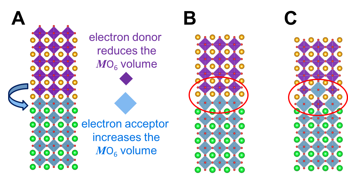
In this sub-section, we discuss antisite defects at oxide interfaces, which turn out to have close connections to charge transfer Chen and Millis (2016); Neumann et al. (2012). Antisite defects in which atoms exchange places across an interface may be important. Here we focus on one particular type of antisite defect: at the interface between two semi-infinite perovskite oxides, two -site transition metal ions interchange their positions. As Fig. 16A shows, if substantial charge transfer occurs across the interface, the O6 oxygen octahedron that donates the electron shrinks its volume, while the O6 oxygen octahedron that accepts the electron expands its volume. If the interface remains atomically sharp as in Fig. 16B, some O6 oxygen octahedra (electron donors) are under tensile strain, while other O6 oxygen octahedra (electron acceptors) are under compressive strain. However, if antisite defects are induced at the interface (see Fig. 16C), the volume disproportionation will be naturally accommodated, which thus significantly reduces the internal strain. This indicates that significant charge transfer across oxide interfaces is a fundamental thermodynamic driving force to induce antisite defects.
In Ref. Chen and Millis (2016), the authors use first-principles methods to survey 21 LaO3/LaO3 interfaces ( = Ti, V, Cr, Mn, Fe, Co, Ni) and 15 SrO3/SrO3 interfaces ( = Ti, V, Cr, Mn, Fe, Co). The authors find that about 50% of the surveyed interfaces have strong tendency for antisite defects and these interfaces have a high degree of charge transfer between two dissimilar transition metal ions.
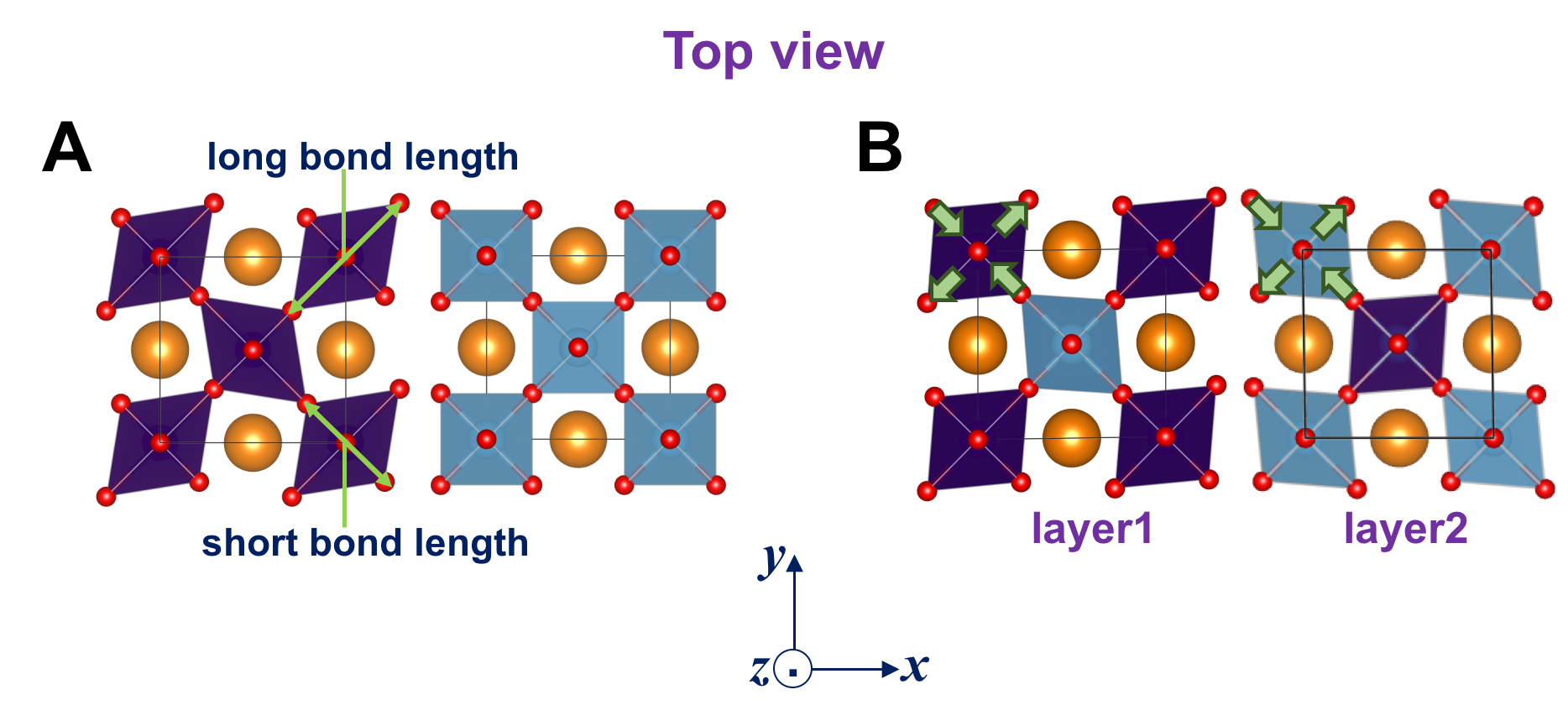
Ref. Chen and Millis (2016) also shows that for interfaces with negligible charge transfer, the presence of Jahn-Teller distortions can help inhibit antisite defects. Fig. 17 shows the effects of Jahn-Teller distortions at oxide interfaces. Panel A) shows the top view of two vertically adjacent oxide layers at the interface without no antisite defects. The purple oxygen octahedron has strong Jahn-Teller distortions (one long metal-oxygen bond length and one short metal-oxygen bond length). The blue oxygen octahedron has no Jahn-Teller distortions (two metal-oxygen bond lengths are equal). Panel B) shows the top view of two vertical adjacent oxide layers at the interface with one antisite defect. The purple oxygen octahedron has bond disproportionation (Jahn-Teller distortion) and the blue oxygen octahedron does not have bond disproportionation. Compatibility with the geometry imposes strains (green arrows) to reduce the bond disproportionation of the purple oxygen octahedron and to induce a bond disproportionation in the blue oxygen octahedron. To reduce the elastic strain, the ideal interface with no antisite defects is thermodynamically favored.
We summarize that antisite defects are strongly associated with geometry constraints, which in turn are controlled by the charge states of transition metal ions and are therefore closely connected to charge transfer. Antisite defects are favored at oxide interfaces if the defect allows the system to accomodate volume disproportionation induced by charge transfer. On the other hand, if the ideal (un-defected) interface can accomodate bond disproportionation due to Jahn-Teller distortions (perhaps also due to charge transfer), antisite defects are disfavored.
VI Theoretical challenges
In this section, we briefly review the theoretical methods that are used to calculate oxide heterostructures and discuss the challenges faced in order to better understand charge-transfer-driven phenomena at oxide interfaces.
The key quantities to calculate are the band alignments between occupied and unoccupied states in bulk materials and between similar states on opposite sides of an interface. Therefore, the biggest challenge is to develop a method with no fitting parameters that calculates electronic structure of realistic materials (including complex heterostructures).
Currently, density functional theory (DFT) Hohenberg and Kohn (1964); Kohn and Sham (1965) with local density approximation (LDA) Perdew and Zunger (1981) and generalized gradient approximation (GGA) Perdew et al. (1996) is the workhorse to calculate the crystal structure of oxide heterostructures. Because this method gives access to the energy as a function of atomic positions, it can capture complicated distortions in oxides, including oxygen octahedral rotations, ferroelectric displacements and metal-oxygen bond disproportionation. However, DFT is a ground state theory which (with the exact exchange correlation functional) yields the correct ground state energy, its charge density and crystal structure (after atomic relaxation). The DFT-calculated electronic structure (band structure and density of state) that is based on fictitious Kohn-Sham orbitals is in principle unphysical and therefore band alignment need not be correct. In practice, for weakly correlated materials such as band insulators, the DFT-calculated electronic structure is qualitatively reasonable, but quantitatively it underestimates the size of band gaps by 30-50%. However, for strongly correlated materials including transition metal oxides, the DFT-calculated electronic structure can be qualitatively incorrect (DFT predicts a metallic ground state for various Mott insulators). Since DFT can not accurately calculate energy separation between metal and oxygen states in many strongly correlated oxides, in oxide heterostructures DFT can also make incorrect predictions on the band alignment of states between two different transition metal atoms, which is the key variable to control charge transfer phenomena.
In order to improve the electronic structure calculated by DFT, various extensions and more sophisticated many-body theory methods have been used in literature. One of the most widely used extension is DFT plus Hubbard and Hund’s corrections, commonly known as the DFT+ method Liechtenstein et al. (1995); Dudarev et al. (1998). In this method, the correlation effects are treated in a static mean-field approximation. The biggest advantage of this method is that its computational scaling is almost the same as standard DFT calculations and atomic relaxation can be performed within the method. However, Hubbard and Hund’s are element-dependent and are fixed phenomenologically. More importantly, DFT+ method is a static mean field approximation that can not describe many important dynamical correlated phenomena, such as the Mott insulating state. DFT plus dynamical mean field theory (DFT+DMFT) is another major extension of DFT Georges et al. (1996); Kotliar et al. (2006). In DFT+DMFT method, DFT calculates the hopping matrix elements of the underlying lattice model for realistic materials, while single-site DMFT calculates a frequency-dependent self energy and the corresponding spectral functions. DFT+DMFT method can describe many dynamical correlated phenomena, such as Mott state and correlation-driven band reduction. More importantly, if Hubbard and Hund’s parameters are correct, the band alignment based on the DMFT-calculated spectral functions is more accurate and reliable than that based on the DFT-calculated density of states. However, like DFT+, DFT+DMFT method itself does not calculate the element-dependent and . Furthermore, the calculation of forces on atoms in complex solids within the DMFT method is still in infancy Chakhalian et al. (2014); Leonov et al. (2014); Haule and Pascut (2016). Therefore unlike DFT+ method, atomic relaxation is not feasible in DFT+DMFT method at this stage. Another important issue in both DFT+ and DFT+DMFT is the double counting problem. In both methods, the separation of DFT and extension raises the possibility that some interactions will be included in both parts and will therefore be counted twice, necessitating the subtraction of an additional “double counting” term. The physical properties calculated from DFT+ or DFT+DMFT sensitively depend on double counting, but unfortunately the exact form of double counting is unknown. In literature a widely used empirical double counting form is called fully localized limit (FLL) Czyżyk and Sawatzky (1994). However, recent work Park et al. (2014) shows that the FLL double counting may lead to an inaccurate energy separation between metal and oxygen states in rare earth nickelates. However, how to improve the FLL counting in DFT+ and DFT+DMFT calculations is one of the biggest theoretical challenges of the methods.
Another two methods–hybrid functional Kümmel and Kronik (2008) and GW Hedin (1965)–have also been used in literature to calculate the electronic structure of complex oxides as an improvement over DFT. The advantage of both methods is that they do not involve material-dependent parameters but both methods are very computationally intensive. Therefore the calculations using both methods are constrained to small systems and atomic relaxation is not practically feasible for complex heterostructures.
We note that in many strongly correlated materials, electronic structure and atomic structure are closely related. For example, VO2 undergoes a coupled metal-insulator rutile-monoclinic transition Morin (1959); Barker et al. (1966). While it is still an on-going research topic whether the transition is primarily driven by electronic transition or structural transition, it is a classical example for strongly correlated materials that different atomic structures correspond to distinct electronic structures. For oxide heterostructures, atoms close to the interface generically move away from their positions in bulk constituents and charge transfer phenomenon is strongly coupled to the new atomic positions because they can significantly change the energy separation between metal states and oxygen states as well as hopping matrix elements and band widths Chen and Millis (2016). Currently DFT and DFT+ methods can efficiently calculate forces on atoms in solids and therefore can perform atomic relaxation and obtain optimal atomic positions for complex heterostructures. However, strong correlation effects are either neglected in DFT or treated in a static mean field approximation in DFT+. On the other hand, DMFT/hybrid functional/GW improve the calculations of electronic structure to different extent, but atomic relaxation is very difficult, if not possible, using these sophisticated methods. The compromising approach of using DFT/DFT+ to obtain the optimal atomic structure or simply using experimentally determined atomic structure, and then using DMFT/hybrid functional/GW methods to calculate electronic structure is currently preferred. A unified theory which can calculate both electronic and atomic structures for strongly correlated materials on the same footing is highly desirable but very challenging. We finally note that while the calculation of many-body band offsets is a key theoretical challenge, measurements of charge transfer and band offsets in experiment can provide a key test of theories.
VII Summary and Perspectives
We reviewed three major mechanisms for charge transfer in oxide heterostructures. In our classification, charge transfer can occur across oxide interfaces in order to compensate for 1) polarity difference, 2) occupancy difference and 3) electronegativity difference between two different transition metal oxides. We summarized representative examples for the first two mechanisms and present a more detailed review of important examples for the third mechanism. Table 1 provides a quick summary. We also reviewed the theoretical methods used to study charge transfer phenomena in oxide heterostructures and discuss the challenges we face in theory.
Oxide heterostructures have shown a plethora of properties which are not exhibited in their bulk constituents. Charge transfer is a very general and robust phenomenon that occurs to oxide interfaces. In the review, we highlight oxide interfaces in which charge transfer occurs to transition metal ions. However, recent experimental progress makes it feasible to synthesize oxide heterostructures that contain and transition metal ions Matsuno et al. (2015). Charge transfer between -to- or -to- transition metal ions is a very interesting direction for future research, since spin-orbit interaction is stronger in and transition metal ions and the interplay between correlation effects and spin-orbit interaction will play a crucial role in charge transfer phenomena. While our review mainly focuses on (001) interfaces, the emergent phenomena identified in oxide heterostructures may also be present in mixed bulk materials, such as double perovskite oxides (e.g. see Section VD). We hope our review can stimulate further theoretical and experimental work to search for novel strongly correlated phenomena in oxide heterostructures.
Acknowledgements.
We are grateful to useful discussion with M. Bibes, H. T. Dang, S. Dong, A. Georges, M. Gibert, C. Marianetti, H. Park, K. Shen, D. Schlom, Z. Zhong and in particular S. Ismail-Beigi. H. Chen is supported by National Science Foundation under Grant No. DMR-1120296. A. J. Millis is supported by the Department of Energy under Grant No. DOE-ER-046169. Computational facilities are provided via Extreme Science and Engineering Discovery Environment (XSEDE), which is supported by National Science Foundation through Grant No. TG-PHY130003 and also via the National Energy Research Scientific Computing Center (NERSC), a DOE Office of Science User Facility supported by the Office of Science of the U.S. Department of Energy.| Mechanisms | Examples | Emergent phenomena |
|---|---|---|
| Polarity difference | LaAlO3/SrTiO3 | The interface is metallic, magnetic and superconducting, although the constituents are insulators in bulk. |
| Occupancy difference | LaTiO3/SrTiO3 | The interface is metallic, although LaTiO3 is a Mott insulator and SrTiO3 is a band insulator . |
| Electro-negativity difference | LaTiO3/LaNiO3 | Ni at the interface is in a Mott insulating state, although Ni in LaNiO3 is in a metallic state. |
| LaTiO3/LaNiO3 /LaAlO3 | Ni at the interface has a huge orbital polarization, although Ni in LaNiO3 has a negligible orbital polarization. | |
| LaMnO3/LaNiO3 | The interface can be either insulating or metallic depending on the thickness of LaMnO3 and LaNiO3, although LaMnO3 is an insulator and LaNiO3 is a metal. | |
| Ba2VFeO6 | Ba2VFeO6 is ferroelectric although both BaVO3 and BaFeO3 have cubic structures (not ferroelectric). | |
| SrVO3/SrMnO3 | Mn at the interface is doped and becomes metallic although SrMnO3 is an insulator. | |
| manganite /cuprate | At the interface the Cu has a multi-orbital Fermi surface, although it is single-band in bulk; and the Mn forms different magnetic domain structures from bulk. |
References
- Y (2012) H. H. I. Y. K. M. K. B. N. N. T. Y, Nat. Mater. 11, 103 (2012).
- Ohtomo and Hwang (2004) A. Ohtomo and H. Y. Hwang, Nature 427, 423 (2004).
- Thiel, S. Hammerl G, Schmehl A, Schneider CW (2006) M. J. Thiel, S. Hammerl G, Schmehl A, Schneider CW, Science (80-. ). 313, 1942 (2006).
- Reyren et al. (2007) N. Reyren, S. Thiel, A. D. Caviglia, L. Fitting Kourkoutis, G. Hammerl, C. Richter, C. W. Schneider, T. Kopp, A.-S. Rüetschi, D. Jaccard, et al., Science (80-. ). 317, 1196 (2007).
- Brinkman et al. (2007) a. Brinkman, M. Huijben, M. van Zalk, J. Huijben, U. Zeitler, J. C. Maan, W. G. van der Wiel, G. Rijnders, D. H. a. Blank, and H. Hilgenkamp, Nat. Mater. 6, 493 (2007).
- Caviglia et al. (2008) A. D. Caviglia, S. Gariglio, N. Reyren, D. Jaccard, T. Schneider, M. Gabay, S. Thiel, G. Hammerl, J. Mannhart, and J.-M. Triscone, Nature 456, 624 (2008).
- Li et al. (2011) L. Li, C. Richter, J. Mannhart, and R. C. Ashoori, Nat. Phys. 7, 762 (2011).
- Bert et al. (2011) J. A. Bert, B. Kalisky, C. Bell, M. Kim, Y. Hikita, H. Y. Hwang, and K. a. Moler, Nat. Phys. 7, 767 (2011).
- Tokura and Hwang (2008) Y. Tokura and H. Y. Hwang, Nat. Mater. 7, 694 (2008).
- Zubko et al. (2011) P. Zubko, S. Gariglio, M. Gabay, P. Ghosez, and J.-M. Triscone, Annu. Rev. Condens. Matter Phys. 2, 141 (2011).
- Chakhalian et al. (2014) J. Chakhalian, J. W. Freeland, A. J. Millis, C. Panagopoulos, and J. M. Rondinelli, Rev. Mod. Phys. 86, 1189 (2014).
- Huijben et al. (2009) M. Huijben, A. Brinkman, G. Koster, G. Rijnders, H. Hilgenkamp, and D. H. A. Blank, Adv. Mater. 21, 1665 (2009).
- Chen et al. (2010a) H. Chen, A. Kolpak, and S. Ismail-Beigi, Adv. Mater. 22, 2881 (2010a).
- Pentcheva and Pickett (2010) R. Pentcheva and W. E. Pickett, J. Phys. Condens. Matter 22, 043001 (2010).
- Shi et al. (2013) Y. Shi, Y. Guo, X. Wang, A. J. Princep, D. Khalyavin, P. Manuel, Y. Michiue, A. Sato, K. Tsuda, S. Yu, et al., Nat. Mater. 12, 1024 (2013).
- Kim et al. (2016) T. H. Kim, D. Puggioni, Y. Yuan, L. Xie, H. Zhou, N. Campbell, P. J. Ryan, Y. Choi, J.-W. Kim, J. R. Patzner, et al., Nature 533, 68 (2016).
- Chen et al. (2010b) H. Chen, A. Kolpak, and S. Ismail-Beigi, Phys. Rev. B 82, 085430 (2010b).
- Millis and Schlom (2010) A. J. Millis and D. G. Schlom, Phys. Rev. B - Condens. Matter Mater. Phys. 82, 073101 (2010).
- Mannhart et al. (2008) J. Mannhart, D. H. A. Blank, H. Y. Hwang, A. J. Millis, and J.-M. Triscone, MRS Bull. 33, 1027 (2008).
- Zaanen et al. (1985) J. Zaanen, G. A. Sawatzky, and J. W. Allen, Phys. Rev. Lett. 55, 418 (1985).
- Nakagawa et al. (2006) N. Nakagawa, H. Y. Hwang, and D. A. Muller, Nat. Mater. 5, 204 (2006).
- Caviglia et al. (2010) A. D. Caviglia, M. Gabay, S. Gariglio, N. Reyren, C. Cancellieri, and J. M. Triscone, Phys. Rev. Lett. 104, 126803 (2010).
- Lesne et al. (2016) E. Lesne, Y. Fu, S. Oyarzun, J. C. Rojas-Sánchez, D. C. Vaz, H. Naganuma, G. Sicoli, J.-P. Attané, M. Jamet, E. Jacquet, et al., Nat. Mater. p. Accepted for Publication (2016).
- Segal et al. (2009) Y. Segal, J. H. Ngai, J. W. Reiner, F. J. Walker, and C. H. Ahn, Phys. Rev. B 80, 241107 (2009).
- Singh-Bhalla et al. (2011) G. Singh-Bhalla, C. Bell, J. Ravichandran, W. Siemons, Y. Hikita, S. Salahuddin, A. F. Hebard, H. Y. Hwang, and R. Ramesh, Nat. Phys. 7, 80 (2011).
- Chen et al. (2009) H. Chen, A. Kolpak, and S. Ismail-Beigi, Phys. Rev. B 79, 161402 (2009).
- Yu and Zunger (2014) L. Yu and A. Zunger, Nat. Commun. 5, 5118 (2014).
- Chambers et al. (2011) S. A. Chambers, L. Qiao, T. C. Droubay, T. C. Kaspar, B. W. Arey, and P. V. Sushko, Phys. Rev. Lett. 107, 206802 (2011).
- Ohtomo et al. (2002) A. Ohtomo, D. A. Muller, J. L. Grazul, and H. Y. Hwang, Nature 419, 378 (2002).
- Okamoto and Millis (2004) S. Okamoto and A. J. Millis, Nature 428, 630 (2004).
- Monkman et al. (2012) E. J. Monkman, C. Adamo, J. a. Mundy, D. E. Shai, J. W. Harter, D. Shen, B. Burganov, D. a. Muller, D. G. Schlom, and K. M. Shen, Nat. Mater. 11, 855 (2012).
- May et al. (2009) S. J. May, P. J. Ryan, J. L. Robertson, J. W. Kim, T. S. Santos, E. Karapetrova, J. L. Zarestky, X. Zhai, S. G. E. te Velthuis, J. N. Eckstein, et al., Nat. Mater. 8, 892 (2009).
- Lüders et al. (2009) U. Lüders, W. C. Sheets, A. David, W. Prellier, and R. Frésard, Phys. Rev. B 80, 241102 (2009).
- Dang and Millis (2013a) H. T. Dang and A. J. Millis, Phys. Rev. B 87, 184434 (2013a).
- Moetakef et al. (2011a) P. Moetakef, T. A. Cain, D. G. Ouellette, J. Y. Zhang, D. O. Klenov, A. Janotti, C. G. Van de Walle, S. Rajan, S. J. Allen, and S. Stemmer, Appl. Phys. Lett. 99, 232116 (2011a).
- Jang et al. (2011) H. W. Jang, D. a. Felker, C. W. Bark, Y. Wang, M. K. Niranjan, C. T. Nelson, Y. Zhang, D. Su, C. M. Folkman, S. H. Baek, et al., Science (80-. ). 331, 886 (2011).
- Moetakef et al. (2012) P. Moetakef, C. A. Jackson, J. Hwang, L. Balents, S. J. Allen, and S. Stemmer, Phys. Rev. B 86, 201102 (2012).
- Chen et al. (2013a) R. Chen, S. Lee, and L. Balents, Phys. Rev. B 87, 161119 (2013a), ISSN 1098-0121.
- Smadici et al. (2007) Å. Smadici, P. Abbamonte, A. Bhattacharya, X. Zhai, B. Jiang, A. Rusydi, J. N. Eckstein, S. D. Bader, and J. M. Zuo, Phys. Rev. Lett. 99, 196404 (2007).
- Bhattacharya et al. (2008) A. Bhattacharya, S. J. May, S. G. E. Te Velthuis, M. Warusawithana, X. Zhai, B. Jiang, J. M. Zuo, M. R. Fitzsimmons, S. D. Bader, and J. N. Eckstein, Phys. Rev. Lett. 100, 257203 (2008).
- Dong et al. (2008) S. Dong, R. Yu, S. Yunoki, G. Alvarez, J. M. Liu, and E. Dagotto, Phys. Rev. B - Condens. Matter Mater. Phys. 78, 201102 (2008).
- Nanda and Satpathy (2009) B. R. K. Nanda and S. Satpathy, Phys. Rev. B 79, 054428 (2009).
- Dang and Millis (2013b) H. T. Dang and A. J. Millis, Phys. Rev. B - Condens. Matter Mater. Phys. 87, 155127 (2013b).
- Imada (1998) M. Imada, Rev. Mod. Phys. 70, 1039 (1998).
- Salamon and Jaime (2001) M. B. Salamon and M. Jaime, Rev. Mod. Phys. 73, 583 (2001).
- Moetakef et al. (2011b) P. Moetakef, T. a. Cain, D. G. Ouellette, J. Y. Zhang, D. O. Klenov, A. Janotti, C. G. Van De Walle, S. Rajan, S. J. Allen, and S. Stemmer, Appl. Phys. Lett. 99, 1 (2011b).
- Yoshimatsu et al. (2010) K. Yoshimatsu, T. Okabe, H. Kumigashira, S. Okamoto, S. Aizaki, A. Fujimori, and M. Oshima, Phys. Rev. Lett. 104, 147601 (2010).
- Boris et al. (2011) A. V. Boris, Y. Matiks, E. Benckiser, A. Frano, P. Popovich, V. Hinkov, P. Wochner, M. Castro-Colin, E. Detemple, V. K. Malik, et al., Science 332, 937 (2011).
- Stemmer and Millis (2013) S. Stemmer and A. J. Millis, MRS Bull. 38, 1032 (2013).
- Chen et al. (2013b) H. Chen, A. Millis, and C. Marianetti, Phys. Rev. Lett. 111, 116403 (2013b).
- Cao et al. (2016) Y. Cao, X. Liu, M. Kareev, D. Choudhury, S. Middey, D. Meyers, J. W. Kim, P. Ryan, J. W. Freeland, and J. Chakhalian, Nat. Commun. 7, 10418 (2016).
- Grisolia et al. (2016) M. N. Grisolia, J. Varignon, G. Sanchez-Santolino, A. Arora, S. Valencia, M. Varela, R. Abrudan, E. Weschke, E. Schierle, J. E. Rault, et al., Nat. Phys. 12, 484 (2016).
- Chen et al. (2013c) H. Chen, D. Kumah, A. Disa, F. Walker, C. Ahn, and S. Ismail-Beigi, Phys. Rev. Lett. 110 (2013c).
- Chaloupka and Khaliullin (2008) J. Chaloupka and G. Khaliullin, Phys. Rev. Lett. 100, 016404 (2008).
- Hansmann et al. (2009) P. Hansmann, X. Yang, A. Toschi, G. Khaliullin, O. K. Andersen, and K. Held, Phys. Rev. Lett. 103, 016401 (2009).
- Disa et al. (2015) A. Disa, D. Kumah, A. Malashevich, H. Chen, D. Arena, E. Specht, S. Ismail-Beigi, F. Walker, and C. Ahn, Phys. Rev. Lett. 114, 026801 (2015).
- Fabbris et al. (2016) G. Fabbris, D. Meyers, J. Okamoto, J. Pelliciari, A. S. Disa, Y. Huang, Z. Y. Chen, W. B. Wu, C. T. Chen, S. Ismail-Beigi, et al., Phys. Rev. Lett. 117 (2016).
- Kleibeuker et al. (2014) J. E. Kleibeuker, Z. Zhong, H. Nishikawa, J. Gabel, A. Müller, F. Pfaff, M. Sing, K. Held, R. Claessen, G. Koster, et al., Phys. Rev. Lett. 113, 237402 (2014).
- Zhang et al. (2015) H. Zhang, Y. Weng, X. Yao, and S. Dong, Phys. Rev. B 91, 195145 (2015).
- Zhong and Hansmann (2016) Z. Zhong and P. Hansmann (2016), eprint 1611.08689, URL http://arxiv.org/abs/1611.08689.
- Hoffman et al. (2013) J. Hoffman, I. C. Tung, B. B. Nelson-Cheeseman, M. Liu, J. W. Freeland, and A. Bhattacharya, Phys. Rev. B 88, 144411 (2013).
- Di Pietro et al. (2015) P. Di Pietro, J. Hoffman, A. Bhattacharya, S. Lupi, and A. Perucchi, Phys. Rev. Lett. 114, 156801 (2015).
- Lee and Han (2013) A. T. Lee and M. J. Han, Phys. Rev. B 88, 035126 (2013).
- Das et al. (2008) H. Das, U. V. Waghmare, T. Saha-Dasgupta, and D. D. Sarma, Phys. Rev. Lett. 100, 186402 (2008).
- Singh et al. (2007) M. P. Singh, K. D. Truong, and P. Fournier, Appl. Phys. Lett. 91, 042504 (2007).
- Singh et al. (2009) M. P. Singh, K. D. Truong, S. Jandl, and P. Fournier, Phys. Rev. B 79, 224421 (2009).
- Chen and Millis (2016) H. Chen and A. Millis, Phys. Rev. B 93, 104111 (2016).
- Gibert et al. (2012) M. Gibert, P. Zubko, R. Scherwitzl, J. Íñiguez, and J.-M. Triscone, Nat. Mater. 11, 195 (2012).
- Gibert et al. (2016) M. Gibert, M. Viret, P. Zubko, N. Jaouen, J.-M. Tonnerre, A. Torres-Pardo, S. Catalano, A. Gloter, O. Stéphan, and J.-M. Triscone, Nat. Commun. 7, 11227 (2016).
- Wu et al. (2011) X. Wu, K. M. Rabe, and D. Vanderbilt, Phys. Rev. B 83, 020104 (2011).
- Chen and Millis (2017) H. Chen and A. J. Millis, under Rev. (2017).
- Chen et al. (2014) H. Chen, H. Park, A. Millis, and C. Marianetti, Phys. Rev. B 90, 245138 (2014).
- Lee et al. (2013) C.-H. Lee, N. D. Orloff, T. Birol, Y. Zhu, V. Goian, E. Rocas, R. Haislmaier, E. Vlahos, J. a. Mundy, L. F. Kourkoutis, et al., Nature 502, 532 (2013).
- Chakhalian et al. (2007) J. Chakhalian, J. W. Freeland, H.-U. Habermeier, G. Cristiani, G. Khaliullin, M. van Veenendaal, and B. Keimer, Science 318, 1114 (2007).
- Chakhalian et al. (2006) J. Chakhalian, J. W. Freeland, G. Srajer, J. Strempfer, G. Khaliullin, J. C. Cezar, T. Charlton, R. Dalgliesh, C. Bernhard, G. Cristiani, et al., Nat. Phys. 2, 244 (2006).
- Neumann et al. (2012) R. F. Neumann, M. Bahiana, and N. Binggeli, EPL (Europhysics Lett. 100, 67002 (2012).
- Hohenberg and Kohn (1964) P. Hohenberg and W. Kohn, Phys. Rev. 136, B864 (1964).
- Kohn and Sham (1965) W. Kohn and L. J. Sham, Phys. Rev. 140, A1133 (1965).
- Perdew and Zunger (1981) J. P. Perdew and A. Zunger, Phys. Rev. B 23, 5048 (1981).
- Perdew et al. (1996) J. P. Perdew, K. Burke, and M. Ernzerhof, Phys. Rev. Lett. 77, 3865 (1996).
- Liechtenstein et al. (1995) A. I. Liechtenstein, V. I. Anisimov, and J. Zaanen, Phys. Rev. B 52, R5467 (1995).
- Dudarev et al. (1998) S. Dudarev, G. Botton, S. Savrasov, C. Humphreys, and A. Sutton, Phys. Rev. B 57, 1505 (1998).
- Georges et al. (1996) A. Georges, G. Kotliar, W. Krauth, and M. J. Rozenberg, Rev. Mod. Phys. 68, 13 (1996).
- Kotliar et al. (2006) G. Kotliar, S. Y. Savrasov, K. Haule, V. S. Oudovenko, O. Parcollet, and C. A. Marianetti, Rev. Mod. Phys. 78, 865 (2006).
- Leonov et al. (2014) I. Leonov, V. I. Anisimov, and D. Vollhardt, Phys. Rev. Lett. 112, 146401 (2014).
- Haule and Pascut (2016) K. Haule and G. L. Pascut, Phys. Rev. B 94, 195146 (2016).
- Czyżyk and Sawatzky (1994) M. T. Czyżyk and G. A. Sawatzky, Phys. Rev. B 49, 14211 (1994).
- Park et al. (2014) H. Park, A. J. Millis, and C. A. Marianetti, Phys. Rev. B 89, 245133 (2014).
- Kümmel and Kronik (2008) S. Kümmel and L. Kronik, Rev. Mod. Phys. 80, 3 (2008).
- Hedin (1965) L. Hedin, Phys. Rev. 139, A796 (1965).
- Morin (1959) F. J. Morin, Phys. Rev. Lett. 3, 34 (1959).
- Barker et al. (1966) A. S. Barker, H. W. Verleur, and H. J. Guggenheim, Phys. Rev. Lett. 17, 1286 (1966).
- Matsuno et al. (2015) J. Matsuno, K. Ihara, S. Yamamura, H. Wadati, K. Ishii, V. V. Shankar, H.-Y. Kee, and H. Takagi, Phys. Rev. Lett. 114, 247209 (2015).