A linear triple quantum dot system in isolated configuration
Abstract
The scaling up of electron spin qubit based nanocircuits has remained challenging up to date and involves the development of efficient charge control strategies. Here we report on the experimental realization of a linear triple quantum dot in a regime isolated from the reservoir. We show how this regime can be reached with a fixed number of electrons. Charge stability diagrams of the one, two and three electron configurations where only electron exchange between the dots is allowed are observed. They are modelled with established theory based on a capacitive model of the dot systems. The advantages of the isolated regime with respect to experimental realizations of quantum simulators and qubits are discussed. We envision that the results presented here will make more manipulation schemes for existing qubit implementations possible and will ultimately allow to increase the number of tunnel coupled quantum dots which can be simultaneously controlled.
Electrons trapped in laterally defined quantum dots (QD) have emerged as a versatile platform for qubit implementationsLoss and DiVincenzo (1998); Hanson et al. (2007); Shulman et al. (2012); Zwanenburg et al. (2013) as well as mesoscopic physics test-beds,Goldhaber-Gordon et al. (1998); Cronenwett, Oosterkamp, and Kouwenhoven (1998); Jeong, Chang, and Melloch (2001) and have recently attracted attention as a possible candidate for quantum simulators.Barthelemy and Vandersypen (2013) Single electron charges and their spin can nowadays be routinely trapped, manipulated and read out in single- and double-QD systems.Hanson et al. (2007); Veldhorst et al. (2014) An important experimental effort has been carried out on multidot systems and charge control of arrays made of up to four tunnel-QDs has been demonstrated. Studenikin et al. (2006); Schröer et al. (2007); Thalineau et al. (2012); Takakura et al. (2014); Eng et al. (2015); Baart et al. (2016) As far as spin is concerned, a triangular triple QD showed charge frustration in transport measurements,Seo et al. (2013) hinting at the possibility of studying spin frustration in such a system and coherent oscillations of three spin states were demonstrated in a linear triple QD.Laird et al. (2010); Gaudreau et al. (2012); Noiri et al. (2016) Despite the inherent scaling properties of lithographically defined semiconductor based systems, the coupling of the QDs with the electron reservoir implies an infinite number of possible charge configurations. The resulting complexity in the dot array tunability limits the capabilities to control simultaneously an increasing number of tunnel-coupled quantum dots and represents an important challenge for large-scale spin-based quantum information processing.
In this study, we apply our recently developed technique of isolated charge manipulationBertrand et al. (2015); Flentje et al. (2017) to a linear chain of three quantum dots. In this regime, the coupling to the electron reservoir can be neglected and only interdot charge transitions are allowed. As a result of the reduced complexity, all possible charge configurations at a fixed electron number are easily accessible and the tunnel-coupling between the dots can be controlled over several orders of magnitude in situ while keeping the electron number fixed. We show how we can bring the linear-triple dot system into an isolated regime, and that the electron number can be prepared deterministically and kept for an arbitrarily long time. The observed charge stability diagrams are analyzed with a model based on the established constant interaction model van der Wiel et al. (2002) and one obtains a good agreement between theory and experiment. These results provide a guideline for scaling up the number of tunnel-coupled QDs, opening up manipulation schemes for qubit implementations, and presenting pathways for the realization of quantum simulators with quantum dot arrays.

Our device was fabricated using a Si doped AlGaAs/GaAs heterostructure grown by molecular beam epitaxy, with a two-dimensional electron gas (2DEG) 100 below the crystal surface which has a carrier mobility of and an electron density of . QDs are defined and controlled by the application of negative voltages on Ti/Au Schottky gates deposited on the surface of the crystal. A schematic view of the linear-triple dot sample can be seen in Fig. 1(a). By applying very negative voltages on diagonally opposite bottom and top blue gates, we can tune the sample into a linear chain of three QDs as indicated in the electrostatic potential calculation of Fig. 1(b).Davies, Larkin, and Sukhorukov (1995); Bautze et al. (2014) Home-made electronics ensure fast changes of both chemical potentials and tunnel-couplings with voltage pulse rise times below 2 . The charge configuration can be read out by four quantum point contacts (QPC), tuned to be sensitive local electrometers.Field et al. (1993) The sample is mounted in a home-made dilution cryostat with an electron temperature of 150 m, estimated from Coulomb peak broadening.Foxman et al. (1994); Meir, Wingreen, and Lee (1991)
The isolation of the electrons is achieved by increasing the tunnel barriers to the leads with more negative voltages on the barrier gates (blue in Fig. 1(a)). To access the isolated regime, a specific voltage sequence needs to be performed. We first reset the number of electrons in the QD 1 to zero at the position R (see Fig. 2(c)), and then load the QD 1 in a position of high tunneling with the leads, close to the point A. By changing the position A, we can load the quantum dot with any number of electron. The system is then disconnected from the leads with a fast voltage pulse on towards point B (black arrows in Fig. 2(c)) which rapidly raises the potential barrier between the quantum dot and the electron reservoir such that the electron number is preserved. A schematic of the potential at the points A and B is shown in Fig. 2(a). Starting from point B, the parameter space is explored by varying the chemical potentials of the individual QDs with and . More precisely, for different , is scanned from negative to positive gate voltages. For more positive than -0.6V, electron exchange between the dots and the reservoir is possible and leads to changes of electron number in the dot, which are detected as peaks in the differential conductance of the electrometer. This corresponds to the blue charge degeneracy lines in the stability diagram as can be seen in the top of Fig. 2(c). These lines separate the charge regions of QD1 and are used to calibrate where to tune the point A to load an arbitrary number of electrons. For more negative than -0.6V, the charge degeneracy line disappears, showing that the dwell time of an electron in the QD becomes much larger than the measurement time and the system becomes effectively decoupled from the reservoir. In other terms, the only allowed charge transitions for electrons are between adjacent QDs. These interdot electron tunnel events will change the detector QPC current similarly to classical charge degeneracy lines and can therefore be detected as shown in the lower part of Fig. 2(c). We note that the timescale for the -scan is several seconds, confirming that an electron can be kept isolated in the QD for a long duration. The result of the isolation procedure manifests itself directly on the stability diagram presented in Fig. 2(c).
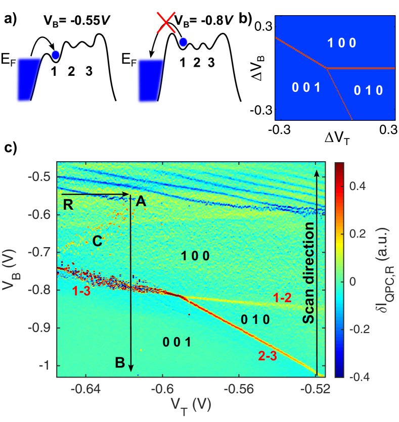
In the case of one-electron-loading, we observe three distinct degeneracy lines indicating charge transitions between QDs. Their slopes permit to label the three obtained charge configurations. For more positive voltages on the gates and (see Fig. 1), the electron is confined in the loading QD 1 (see Fig. 2(a)). We label this configuration (1 0 0) indicating the number of electrons in the respective QDs. By making the voltage on more negative, it is possible to move the electron into QD 2 (0 1 0). For very negative voltages on both gates, the electron is moved to QD 3 (0 0 1). As expected from the sample geometry, the voltage strongly affects the height of the energy barrier between QD 1 and QD 2 and therefore the tunnel-coupling between the respective QDs. For positive values of , this increased tunnel-coupling leads to a broadening of the associated degeneracy line.DiCarlo et al. (2004) Conversely, the QD 2- QD 3 degeneracy line is almost unaffected by . Due to linear configuration of the dot array, the electron tunneling process between QD 1 and QD 3 is the result of an indirect coupling mediated by the QD 2.Braakman et al. (2013); Takakura et al. (2014) As a consequence, we expect a strong dependence of the associated energy with the two direct tunnel-couplings (QD 1-QD 2 and QD 2-QD 3) as well as the energy detuning with the chemical potential of QD 2. In the geometry of the sample, both the QD 1-QD 2 coupling and the detuning are controlled by . It explains the observed fast change of the QD 1-QD 3 degeneracy line shape suggesting the QD 1-QD 3 tunnel-coupling going to zero for smaller than -0.6V.
Despite these strong changes in the tunneling rate, the transition lines in the stability diagram stay clearly visible over a large parameter range showing the insensitivity of this approach to an initially unknown coupling strength. It nevertheless disappears in two regimes: when the tunneling time becomes much longer than the measurement time such that the events become stochastic (Hz; left of in Fig. 2(c)). Secondly, it disappears in the limit where the tunneling energy becomes much larger than temperature (GHz), and therefore the line broadens until no longer being observable (right part of Fig. 2(c)). Moreover, the QD 1-QD 2 tunnel-coupling can then be continuously varied by changing without erroneously changing the electron number. This controlled variability of the tunnel-coupling in the isolated regime has recently been used to implement a spin manipulation scheme which is partially protected from charge noise.Bertrand et al. (2015)
To show the straightforwardness of this approach for scaling-up the occupation number, we load the triple QD with two or three electrons, and perform the same gate scans (Fig. 3(a,b)). Similar to the one electron case, the isolated degeneracy lines are characterized by the same three slopes and the different charge configurations are therefore assigned as represented in Fig 2.
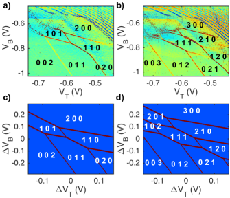
Furthermore, we can quantitatively understand the structure formed by the transition lines with the constant interaction model.Van Houten, Beenakker, and Staring (1992); Hanson et al. (2007) In the electrostatic model presented in Fig. 4, the coupling between electrons in the QDs and the gates is modelled as a sum of capacitances. We first introduce the renormalized gate capacitances to parametrize the effect of gate voltage on the potential of QD . Then the energy of the charge configurations (i.e. for , (1 0 0)) is given by Van Houten, Beenakker, and Staring (1992)
| (1) |
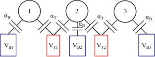
where the summation is over all QDs , is the charging energy of QD and is the number of electrons compensating the positive donor charges which are related to the electron density of the 2DEG. As the electron reservoirs can no longer be used as chemical potential references, has to be limited to the subspace of configurations with constant total electron charges and the smallest will be the ground state. In the model, we neglect the finite capacitive coupling between QDs and the dot orbital energies. These effects do not change the shape of the diagram, but only renormalize the involved capacitances and charging energies. The boundaries between the energetically lowest lying charge configurations as a function of the gate voltages has been plotted for different total number of electrons in Fig. 2(b) and Fig. 3(c,d) and show an excellent qualitative agreement with the experimental data. At a degeneracy line the energy of the two associated quantum dot configurations is equal. The respective slopes of the transitions in the experimental diagrams therefore allow to infer the ratios / for the respective QDs. The absolute values can in principle be measured using transport measurements or photon-assisted tunnelingOosterkamp et al. (1998) (possible in the isolated regime). Here we got quantitative agreement by guessing one parameter () and neglecting any influence of and on QD 3 (see Fig. 4). The charging energies of the QDs are determined by the positions of the parallel charge degeneracy line crossings in the diagram with two electrons (Fig. 3(a)).
The reduced complexity of the obtained charge diagrams can be harnessed for the operation of large quantum dot systems. As electrons can access all configurations without unwanted electron exchange with the reservoirs due to pulse imperfections, this approach of fixed electron number manipulation allows to increase the effective size of the available configuration space. The isolation also allows to study the behavior of systems in which an increasing number of QDs prevents the more distant leads to be used as an effective chemical potential reference.
In conclusion, we have performed a full control sequence for a multidot system decoupled from the leads. We have demonstrated how the system can be initialized with a desired number of electrons, and that all possible charge configurations can be easily accessed with the same electrons. The resulting system can be understood and modelled with established theory and shows qualitative and quantitative consistency with the measured diagrams. The reduced complexity of the isolated regime makes charge reorganization in the structure straightforward and permit higher tunability of the dot parameters. We conclude that this approach will allow to increase the size of multiqubit systems as well as open up manipulation schemes for existing systems. Finally, the concept of isolated charge manipulation can be directly extended to similar qubit architectures such as electron spins in silicon, and should therefore find wide application in future experiments.
Acknowledgements.
We acknowledge technical support from the “Poles Electroniques” of the “Département Nano and MCBT” from the Institut Néel as well as Henry Rodenas for technical support. A.D.W. acknowledges support of the DFG SPP1285 and the BMBF QuaHLRep 01BQ1035. T.M. acknowledges financial support ERC ”QSPINMOTION” (307149). We are grateful to the Nanoscience Foundation of Grenoble, for partial financial support of this work. Devices were fabricated at “Plateforme Technologique Amont” de Grenoble, with the financial support of the “Nanosciences aux limites de la Nanoélectronique” Foundation and CNRS Renatech network.References
- Loss and DiVincenzo (1998) D. Loss and D. P. DiVincenzo, Phys. Rev. A 57, 120 (1998).
- Hanson et al. (2007) R. Hanson, L. P. Kouwenhoven, J. R. Petta, S. Tarucha, and L. M. K. Vandersypen, Rev. Mod. Phys. 79, 1217 (2007).
- Shulman et al. (2012) M. D. Shulman, O. E. Dial, S. P. Harvey, H. Bluhm, V. Umansky, and A. Yacoby, Science 336, 202 (2012).
- Zwanenburg et al. (2013) F. A. Zwanenburg, A. S. Dzurak, A. Morello, M. Y. Simmons, L. C. Hollenberg, G. Klimeck, S. Rogge, S. N. Coppersmith, and M. A. Eriksson, Reviews of modern physics 85, 961 (2013).
- Goldhaber-Gordon et al. (1998) D. Goldhaber-Gordon, H. Shtrikman, D. Mahalu, D. Abusch-Magder, U. Meirav, and M. Kastner, Nature 391, 156 (1998).
- Cronenwett, Oosterkamp, and Kouwenhoven (1998) S. M. Cronenwett, T. H. Oosterkamp, and L. P. Kouwenhoven, Science 281, 540 (1998).
- Jeong, Chang, and Melloch (2001) H. Jeong, A. M. Chang, and M. R. Melloch, Science 293, 2221 (2001).
- Barthelemy and Vandersypen (2013) P. Barthelemy and L. M. K. Vandersypen, Ann. Phys. 525, 808 (2013).
- Veldhorst et al. (2014) M. Veldhorst, J. Hwang, C. Yang, A. Leenstra, B. De Ronde, J. Dehollain, J. Muhonen, F. Hudson, K. M. Itoh, A. Morello, et al., Nature nanotechnology 9, 981 (2014).
- Studenikin et al. (2006) S. Studenikin, L. Gaudreau, A. Sachrajda, P. Zawadzki, A. Kam, J. Lapointe, M. Korkusinski, and P. Hawrylak, in Nanotechnology, 2006, Vol. 2 (IEEE, 2006) pp. 871–874.
- Schröer et al. (2007) D. Schröer, A. D. Greentree, L. Gaudreau, K. Eberl, L. C. L. Hollenberg, J. P. Kotthaus, and S. Ludwig, Phys. Rev. B 76, 075306 (2007).
- Thalineau et al. (2012) R. Thalineau, S. Hermelin, A. D. Wieck, C. Bäuerle, L. Saminadayar, and T. Meunier, Appl. Phys. Lett. 101, 103102 (2012).
- Takakura et al. (2014) T. Takakura, A. Noiri, T. Obata, T. Otsuka, J. Yoneda, K. Yoshida, and S. Tarucha, Appl. Phys. Lett. 104, 113109 (2014).
- Eng et al. (2015) K. Eng, T. D. Ladd, A. Smith, M. G. Borselli, A. A. Kiselev, B. H. Fong, K. S. Holabird, T. M. Hazard, B. Huang, P. W. Deelman, I. Milosavljevic, A. E. Schmitz, R. S. Ross, M. F. Gyure, and A. T. Hunter, Science Advances 1 (2015).
- Baart et al. (2016) T. A. Baart, M. Shafiei, T. Fujita, C. Reichl, W. Wegscheider, and V. L. M. K., Nat. Nano 11, 330 (2016).
- Seo et al. (2013) M. Seo, H. K. Choi, S.-Y. Lee, N. Kim, Y. Chung, H.-S. Sim, V. Umansky, and D. Mahalu, Phys. Rev. Lett. 110, 046803 (2013).
- Laird et al. (2010) E. A. Laird, J. M. Taylor, D. P. DiVincenzo, C. M. Marcus, M. P. Hanson, and A. C. Gossard, Phys. Rev. B 82, 075403 (2010).
- Gaudreau et al. (2012) L. Gaudreau, G. Granger, A. Kam, G. Aers, S. Studenikin, P. Zawadzki, M. Pioro-Ladriere, Z. Wasilewski, and A. Sachrajda, Nat. Phys. 8, 54 (2012).
- Noiri et al. (2016) A. Noiri, J. Yoneda, T. Nakajima, T. Otsuka, M. R. Delbecq, K. Takeda, S. Amaha, G. Allison, A. Ludwig, A. D. Wieck, et al., Applied Physics Letters 108, 153101 (2016).
- Bertrand et al. (2015) B. Bertrand, H. Flentje, S. Takada, M. Yamamoto, S. Tarucha, A. Ludwig, A. D. Wieck, C. Bäuerle, and T. Meunier, Phys. Rev. Lett. 115, 096801 (2015).
- Flentje et al. (2017) H. Flentje, P. Mortemousque, R. Thalineau, A. Ludwig, A. Wieck, C. Bäuerle, and T. Meunier, arXiv preprint arXiv:1701.01279 (2017).
- van der Wiel et al. (2002) W. G. van der Wiel, S. De Franceschi, J. M. Elzerman, T. Fujisawa, S. Tarucha, and L. P. Kouwenhoven, Rev. Mod. Phys. 75, 1 (2002).
- Davies, Larkin, and Sukhorukov (1995) J. H. Davies, I. A. Larkin, and E. V. Sukhorukov, Journal of Applied Physics 77, 4504 (1995).
- Bautze et al. (2014) T. Bautze, C. Süssmeier, S. Takada, C. Groth, T. Meunier, M. Yamamoto, S. Tarucha, X. Waintal, and C. Bäuerle, Phys. Rev. B 89, 125432 (2014).
- Field et al. (1993) M. Field, C. G. Smith, M. Pepper, D. A. Ritchie, J. E. F. Frost, G. A. C. Jones, and D. G. Hasko, Phys. Rev. Lett. 70, 1311 (1993).
- Foxman et al. (1994) E. B. Foxman, U. Meirav, P. L. McEuen, M. A. Kastner, O. Klein, P. A. Belk, D. M. Abusch, and S. J. Wind, Phys. Rev. B 50, 14193 (1994).
- Meir, Wingreen, and Lee (1991) Y. Meir, N. S. Wingreen, and P. A. Lee, Phys. Rev. Lett. 66, 3048 (1991).
- DiCarlo et al. (2004) L. DiCarlo, H. J. Lynch, A. C. Johnson, L. I. Childress, K. Crockett, C. M. Marcus, M. P. Hanson, and A. C. Gossard, Phys. Rev. Lett. 92, 226801 (2004).
- Braakman et al. (2013) F. R. Braakman, P. Barthelemy, C. Reichl, W. Wegscheider, and L. M. Vandersypen, Nature nanotechnology 8, 432 (2013).
- Van Houten, Beenakker, and Staring (1992) H. Van Houten, C. Beenakker, and A. Staring, in Single charge tunneling (Springer, 1992) pp. 167–216.
- Oosterkamp et al. (1998) T. Oosterkamp, T. Fujisawa, W. Van Der Wiel, K. Ishibashi, R. Hijman, S. Tarucha, and L. P. Kouwenhoven, Nature 395, 873 (1998).