Current enhancement due to field-induced dark carrier multiplication in graphene
Abstract
We present a microscopic study on current generation in graphene in response to an electric field. While scattering is generally considered to reduce the current, we reveal that in graphene Auger processes give rise to a current enhancement via a phenomenon we denote dark carrier multiplication. Based on a microscopic approach, we show that, if other scattering channels are absent, this prevents the carrier distribution to reach a stationary value. Taking into account scattering with phonons a finite current is restored, however its value exceeds the stationary current without scattering.
Transport properties of graphene, in particular the exceptionally high electrical conductivity even at room temperature, have been intensively studied since its discovery Geim and Novoselov (2007); Morozov et al. (2008); Castro Neto et al. (2009); Das Sarma et al. (2011). In early graphene samples, electrical transport was limited by disorder resulting in mobilities of up to at low temperatures Novoselov et al. (2005); Zhang et al. (2005); Mariani and von Oppen (2008). However, it was demonstrated that eliminating the extrinsic disorder, the fundamental limit of the mobility at room-temperature is considerably higher Morozov et al. (2008); Du et al. (2008); Bolotin et al. (2008). Depending on the sample, flexural or in-plane phonons are considered to be responsible for limiting the intrinsic conductivity Katsnelson and Geim (2008); Mariani and von Oppen (2008, 2010); Castro et al. (2010). Moreover, in contrast to conventional materials with a parabolic band structure, carrier-carrier scattering has an impact on the current Kashuba (2008); Fritz et al. (2008); Gornyi et al. (2012); Sun et al. (2012). While most studies in literature focus on the linear response and deploy the Drude approach for the conductivity, there are only a few studies addressing the non-linear response of graphene to an electric field Bistritzer and MacDonald (2009); Balev et al. (2009); Dóra and Moessner (2010); Rosenstein et al. (2010); Tani et al. (2012).
In this work, we provide a microscopic access to the time- and momentum-dependent carrier dynamics in graphene in a constant in-plane electric field. Using the density matrix formalism, we calculate all intrinsic carrier-phonon and carrier-carrier scattering channels within the second-order Born-Markov approximation. This allows us to investigate the temporal evolution of the carrier density as well as the generation and the dynamics of the electrical current giving new insights into carrier transport in graphene. In a many-particle process that we denote as dark carrier multiplication (dark CM), Coulomb-induced processes bridging the valence and the conduction band (Auger scattering) significantly increase the carrier density in response to the electric field. Signatures of this effect have already been found in near-infrared transient absorption measurements under high electric fields using THz excitation pulses Tani et al. (2012). Furthermore, a carrier density increase has been discussed in literature as a consequence of the radiative coupling Balev et al. (2009) or the Schwinger mechanism Dóra and Moessner (2010); Rosenstein et al. (2010). The latter two effects are much weaker at room temperature than Auger processes, which have been demonstrated to be extremely efficient in graphene Winzer et al. (2010); Winzer and Malic (2012); Brida et al. (2013); Plötzing et al. (2014); Mittendorff et al. (2015); Wendler et al. (2014); Gierz et al. (2015). The aim of this work is to investigate the impact of the field-induced dark CM on the generation and enhancement of electric currents in graphene.
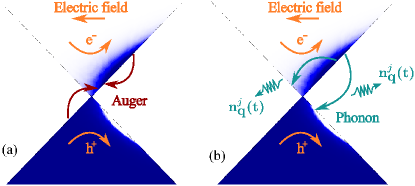
When graphene is placed in an external in-plane electric field , its electrons are accelerated in the direction anti-parallel to the field which we set to be the negative x-direction . This is illustrated in Fig. 1 showing the Dirac cone of graphene including resulting Coulomb- and phonon-induced scattering processes. Since we consider neutral graphene characterized by a vanishing chemical potential, the electron-hole symmetry allows us to focus on the dynamics of electrons in the conduction band. Nevertheless, it is instructive to note that electrons and holes appearing on the same side of the Dirac cone, move into opposite directions in real space, since the electron group velocity is given by with the Fermi velocity and the band index denoting the conduction () and the valence () band, respectively. Therefore, electrons at move into the -direction, and, since a hole is nothing else than a missing electron, it can be represented by an electron moving into the -direction, which corresponds to a positively charged hole moving into the -direction. Hence, the group velocities of electrons and holes are the same, both changing sign when the band is switched. Consequently, the shift of electron and hole occupations to the right in k space, cf. Fig. 1, means that electrons and holes move into opposite directions in real space.
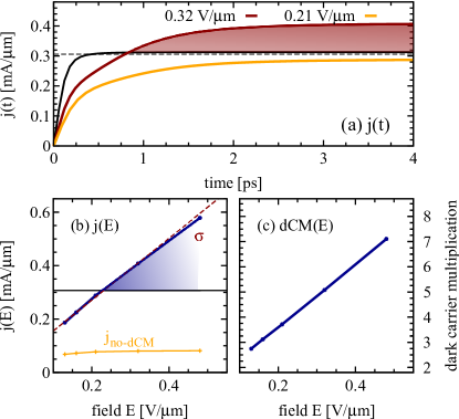
As electrons are accelerated in the electric field, the magnitude of their velocity remains constant and only the direction of their motion changes. Consequently, if scattering channels are switched off, the current density saturates to a finite value corresponding to the situation, in which all electrons move into the direction anti-parallel to the field. The resulting current density dynamics exhibits an initial increase until the equilibrium current density is reached after a few picoseconds, cf. the black line in Fig. 2 (a). While the time scale on which the saturation takes place is given by the field strength , the saturation current density only depends on the initial temperature-dependent carrier density, cf. the black line in Fig. 2(b).
The current density dynamics at room temperature including all scattering channels is shown in Fig. 2(a) for different field strengths . For , the current density saturates, as expected, below the value without scattering suggesting that a certain non-zero resistivity has been introduced. Surprisingly, we reveal that for sufficiently high many-particle scattering processes can even enhance the saturation current density, i.e. they introduce a scattering-induced current density amplification, cf. the red-shaded area in Fig. 2(a). This can be traced back to Auger scattering, which give rise to a significant increase of the charge carrier density. This process bridging the valence and the conduction band (Fig.1(a)) corresponds to the creation of an additional electron-hole pairs which indirectly – via an enhanced carrier density – boosts the generated current density. In analogy to the regular carrier multiplication (CM) induced by an optical excitation Winzer et al. (2010), we define the field-induced dark CM by the ratio of the equilibrium carrier density with () and without () the electric field: . The generated dark CM is shown in Fig. 2(c) as a function of the electric field. Its increased efficiency explains the observed enhancement of the current density at high fields above the saturation value without scattering.
Figure 2(b) demonstrates that Ohm’s law is valid in graphene for small fields, cf. the linear increase with a slope corresponding to a conductivity of . This is larger than experimentally obtained values Novoselov et al. (2005); Zhang et al. (2005); Morozov et al. (2008), since we consider a perfect graphene sample and an idealized situation without any negative influences of the environment. To illustrate that the large conductivity results from the strong impact of the dark CM, we approximate the current density excluding the influence of the dark CM , cf. the yellow line in Fig. 2(b). This approximation is obtained using the relation with the drift velocity (average velocity of charged carriers). Now, the initial carrier density is separated from the dark CM-induced density resulting in . In the absence of dark CM, the current density is much smaller and shows only a minimal increase with the field strength. Most importantly, it always stays well below the saturation current density in the case without scattering.
The mobility can be estimated via the slope of the drift velocity plotted over the electric field yielding in the linear region a value of . It cannot be inferred from the usual relation , where is the elementary charge, since now the carrier density depends on the electric field due to the appearance of dark CM. Instead, using and the generalized definitions of the mobility and the conductivity and , respectively, the relation is found. The reason for the comparably small value of the mobility (despite the rather large conductivity), is the relatively high temperature () corresponding to a large carrier density, which is even enhanced by the dark CM.
Before we go further into detail of the carrier dynamics leading to the enhancement of the current density via many-particle scattering, we first briefly introduce the applied microscopic approach. The many-particle Hamilton operator consists of the (i) free carrier and phonon contribution , (ii) carrier-carrier and (iii) carrier-phonon interaction accounting for Coulomb- and phonon-induced scattering, and (iv) the interaction of an external electric field with carriers. The latter contribution reads for electrons in second quantization Meier et al. (1994)
| (1) |
where , denote creation and annihilation operators for electrons in the band and with the momentum . Evaluating the Heisenberg’s equation of motion and applying the second-order Born-Markov approximation Haug and Koch (2009); Kira and Koch (2006); Malic and Knorr (2013), we obtain the graphene Bloch equations explicitly including the impact of an electric field:
| (2) | ||||
| (3) |
The equations describe the coupled dynamics of the electron occupation probability in the state and the phonon number in the mode with the momentum . The time- and momentum-dependent in- and out-scattering rates contain all relevant carrier-carrier and carrier-phonon scattering channels including acoustic , and optical , , KLO, KTO phonons. The dynamics of the phonon number is determined by the emission and absorption rates driving towards the initial Bose-distribution . The phonon decay rate is adjusted to the experimentally obtained value Kang et al. (2010). For more details on the microscopic origin of the rates, we refer to Refs. Malic and Knorr, 2013; Malic et al., 2011.
The presence of an electric field enters the Bloch equations through the scalar product between the electrical field and the gradient of the carrier occupation , cf. Eq. (2). It stems from the commutation of the carrier-field Hamilton operator from Eq. (1) with . Within the applied Born approximation, the electric field does not influence the lattice positions, hence there is no electric field contribution in Eq. (3). Using the coordinate transformation Meier et al. (1994) , one can transform the Bloch equations according to resulting in regular Bloch equations without the electric field. Here, the field-induced dynamics is hidden in the new field- and time-dependent momenta . This means that we consider a moving coordinate frame describing the electric field-induced shift of the carrier occupation in momentum space. In case of a vanishing electric field , the equilibrium distributions of electrons and phonons and are given by Fermi-Dirac and Bose-Einstein distributions, respectively. When this equilibrium is disturbed by a field , many-particle scattering occurs until new equilibrium distributions emerge. In conventional semiconductors, the carrier densities of the two equilibrium distributions (with and without the field) are the same. In contrast, strongly efficient Auger scattering in graphene results in a carrier density increase, which is quantified by the dark CM 111 Note that for an infinitely extended graphene sheet in an in-plane electric field, electron-hole pairs can also be created due to the Schwinger mechanism Schwinger (1951); Dóra and Moessner (2010); Rosenstein et al. (2010). Here, we restrict our investigation to finite temperatures of , where the field-induced acceleration of thermal charge carriers gives rise to a dark CM that prevails over the Schwinger effect. .
Numerical evaluation of the graphene Bloch equations provides a microscopic access to the coupled time- and momentum-resolved carrier and phonon dynamics under the influence of an electric field and its interplay with Coulomb- and phonon-induced scattering channels. The main observable in our study is the intraband current density which reads under electron-hole symmetry Malic and Knorr (2013)
| (4) |
The appearing area of the graphene flake cancels out after performing the sum over all momenta . The factor 8 describes the spin and valley degeneracy of the electronic states as well as the electron-hole symmetry. The current density can be rephrased in terms of carrier density and drift velocity , where is the electron group velocity. In conventional materials with a parabolic band structure with the effective mass , the group velocity reads , whereas in graphene, it is given by due to its linear bandstructure . Consequently, only the angle between the electronic momentum and the applied electrical field determines the contribution of the carrier occupation to the current density in graphene, while the magnitude of is irrelevant in this regard.
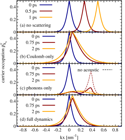
The spectral distribution of the electron occupation is shown in Fig. 3 at room temperature and along the -direction (corresponding to the direction of the applied electric field) at different times and including different scattering channels. The case without scattering demonstrates that the in-plane electric field accelerates the available charge carriers in the k space into the opposite field direction (), cf. Fig. 3(a). Initially without the field, the carrier occupation is fully symmetric in , hence the group velocities of the charge carriers point in different directions resulting in zero drift velocity and current density, cf. Eq. (4). Switching on the electric field (at ), the carriers are shifted resulting in an asymmetric carrier distribution and thus a current density is generated. It increases until the velocity of all charge carriers aligns with the field. The saturation current density sets in already at picosecond time scales and long before the charge carriers leave the linear region of the Brillouin zone, cf. the black line in Fig. 2 (a). The generated saturation current density is independent of the strength of the electric field (Fig. 2(b)) and scales with
| (5) |
where is the Boltzmann constant.
Next, we include all carrier-carrier scattering channels and observe that the distribution is still slightly shifted with respect to the Dirac point and becomes spectrally broader due to Auger scattering, cf. Fig. 3(b). While carrier-carrier scattering does not influence the current in conventional materials, in graphene its impact on the current is twofold: (i) it redistributes charge carriers and thereby induces a resistivity, i.e. current reduction, and (ii) it results in a carrier density increase via Auger processes (i.e. dark CM) giving rise to a current enhancement. While mechanism (i) leads to a carrier distribution resembling a Fermi distribution, which is shifted and distorted along the field direction, mechanism (ii) causes a steady increase of the carrier density without reaching an equilibrium. In contrast, including only carrier-phonon scattering channels, cf. Fig. 3(c), an equilibrium carrier distribution is reached, however, it considerably deviates from a Fermi distribution. While low energetic acoustic phonons play only a minor role for energy relaxation Malic et al. (2011); Winnerl et al. (2011), they have a strong impact on momentum relaxation and thus on the current density, cf. dashed lines in Fig. 3(c). The complete dynamics including both carrier-carrier and carrier-phonon scattering is displayed in Fig. 3(d). Here, the distribution resembles the case of purely Coulomb-induced dynamics. However, now it exhibits an equilibrium due to carrier-phonon scattering competing with Auger processes and stabilizing the carrier density.
As a result, evaluating the graphene Bloch equations, the current density dynamics is revealed on a microscopic footing. It results from the interplay of the field-induced acceleration of charge carriers and Coulomb- and phonon-induced scattering processes. We find current-reducing carrier-carrier and carrier-phonon scattering channels as well as current-enhancing Auger scattering, a specific Coulomb channel giving rise to a dark CM. It is small at low electric fields , but causes a current density increase above the saturation value for , cf. Fig. 2(b).
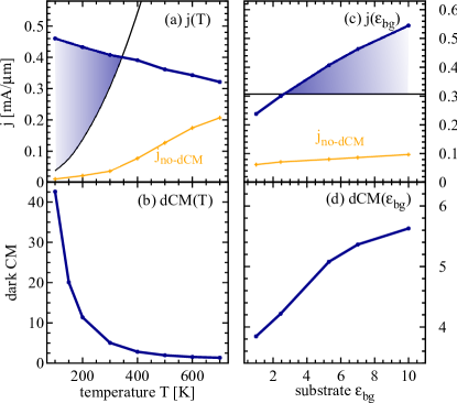
Next, we investigate the dependence of the equilibrium current density on the strength of the carrier phonon scattering and the Coulomb interaction, which can be controlled by varying temperature and substrate, respectively. The substrate is assumed to be only on one side of graphene resulting in an averaged background dielectric constant . The standard substrate used in Figs. 1- 3 is silicon carbide with a static dielectric constant Patrick and Choyke (1970). The crucial point in the temperature- and substrate-dependence of the current density is their influence on the dark CM, cf. blue and yellow lines in Fig. 4(a) and (c), respectively.
The temperature dependence of the dark CM is determined by Pauli blocking, which is small for narrow carrier distributions at low temperatures, cf. Fig. 4(b). To understand the influence of the dark CM on the current density (Fig. 4(a)), we first consider the case without scattering (black line), where the current density is found to scale with according to Eq. (5). Switching on the scattering channels but suppressing the carrier density increase due to the dark CM (yellow line) the current density is strongly reduced, and owing to an enhanced acoustic phonon scattering this reduction increases with the temperature. Due to the pronounced dark CM at low (Fig. 4(b)), a significant current density amplification occurs up to the room temperature (blue-shaded region). For higher temperatures, the dark CM becomes negligible and the efficient scattering with acoustic phonons leads to a saturation of the current density.
The substrate dependence reveals a clear enhancement of the current density and the dark CM at higher dielectric background constants , cf. Figs. 4(c) and (d). A larger screens the Coulomb potential and reduces the efficiency of carrier-carrier scattering. This leads to an enhanced dark CM, since the time window for Auger processes is increased. This resembles the increase of the conventional carrier multiplication at low pump fluences, cf. Ref. Plötzing et al., 2014. Moreover, at low dielectric constants the Coulomb-induced redistribution of charge carriers competing with Auger scattering is suppressed resulting in improved conditions for the dark CM.
In conclusion, we have investigated the impact of the time- and momentum-resolved carrier dynamics on the generation of currents in graphene in the presence of an in-plane electric field. We show that field-induced acceleration of charge carriers provides excellent conditions for Auger scattering, which give rise to a dark carrier multiplication resulting in a significant enhancement of the generated currents. The presented insights are applicably to the entire class of Dirac materials.
Acknowledgements.
This project has received funding from the European Union’s Horizon 2020 research and innovation programme under grant agreement No 696656 (Graphene Flagship). Furthermore, we acknowledge support from the Swedish Research Council (VR) and the Deutsche Forschungsgemeinschaft through SFB 658 and SPP 1459. The computations were performed on resources at Chalmers Centre for Computational Science and Engineering (C3SE) provided by the Swedish National Infrastructure for Computing (SNIC). Finally, we thank Andreas Knorr (TU Berlin) for inspiring discussions.References
- Geim and Novoselov (2007) A. K. Geim and K. S. Novoselov, Nat. Mater. 6, 183 (2007).
- Morozov et al. (2008) S. V. Morozov, K. S. Novoselov, M. I. Katsnelson, F. Schedin, D. C. Elias, J. A. Jaszczak, and A. K. Geim, Phys. Rev. Lett. 100, 016602 (2008).
- Castro Neto et al. (2009) A. H. Castro Neto, F. Guinea, N. M. R. Peres, K. S. Novoselov, and A. K. Geim, Rev. Mod. Phys. 81, 109 (2009).
- Das Sarma et al. (2011) S. Das Sarma, S. Adam, E. H. Hwang, and E. Rossi, Rev. Mod. Phys. 83, 407 (2011).
- Novoselov et al. (2005) K. S. Novoselov, A. K. Geim, S. V. Morozov, D. Jiang, M. I. Katsnelson, I. V. Grigorieva, S. V. Dubonos, and A. A. Firsov, Nature 438, 197 (2005).
- Zhang et al. (2005) Y. Zhang, Y.-W. Tan, H. L. Stormer, and P. Kim, Nature 438, 201 (2005).
- Mariani and von Oppen (2008) E. Mariani and F. von Oppen, Phys. Rev. Lett. 100, 076801 (2008).
- Du et al. (2008) X. Du, I. Skachko, A. Barker, and E. Y. Andrei, Nat. Nano. 3, 491 (2008).
- Bolotin et al. (2008) K. Bolotin, K. Sikes, Z. Jiang, M. Klima, G. Fudenberg, J. Hone, P. Kim, and H. Stormer, Solid State Commun. 146, 351 (2008).
- Katsnelson and Geim (2008) M. Katsnelson and A. Geim, Phil. Trans. R. Soc. A 366, 195 (2008).
- Mariani and von Oppen (2010) E. Mariani and F. von Oppen, Phys. Rev. B 82, 195403 (2010).
- Castro et al. (2010) E. V. Castro, H. Ochoa, M. I. Katsnelson, R. V. Gorbachev, D. C. Elias, K. S. Novoselov, A. K. Geim, and F. Guinea, Phys. Rev. Lett. 105, 266601 (2010).
- Kashuba (2008) A. B. Kashuba, Phys. Rev. B 78, 085415 (2008).
- Fritz et al. (2008) L. Fritz, J. Schmalian, M. Müller, and S. Sachdev, Phys. Rev. B 78, 085416 (2008).
- Gornyi et al. (2012) I. V. Gornyi, V. Y. Kachorovskii, and A. D. Mirlin, Phys. Rev. B 86, 165413 (2012).
- Sun et al. (2012) D. Sun, C. Divin, M. Mihnev, T. Winzer, E. Malic, A. Knorr, J. E. Sipe, C. Berger, W. A. de Heer, P. N. First, and T. B. Norris, New J. Phys. 14, 105012 (2012).
- Bistritzer and MacDonald (2009) R. Bistritzer and A. H. MacDonald, Phys. Rev. B 80, 085109 (2009).
- Balev et al. (2009) O. G. Balev, F. T. Vasko, and V. Ryzhii, Phys. Rev. B 79, 165432 (2009).
- Dóra and Moessner (2010) B. Dóra and R. Moessner, Phys. Rev. B 81, 165431 (2010).
- Rosenstein et al. (2010) B. Rosenstein, M. Lewkowicz, H. C. Kao, and Y. Korniyenko, Phys. Rev. B 81, 041416 (2010).
- Tani et al. (2012) S. Tani, F. Blanchard, and K. Tanaka, Phys. Rev. Lett. 109, 166603 (2012).
- Winzer et al. (2010) T. Winzer, A. Knorr, and E. Malic, Nano Lett. 10, 4839 (2010).
- Winzer and Malic (2012) T. Winzer and E. Malic, Phys. Rev. B 85, 241404 (2012).
- Brida et al. (2013) D. Brida, A. Tomadin, C. Manzoni, Y. J. Kim, A. Lombardo, S. Milana, R. R. Nair, K. S. Novoselov, A. C. Ferrari, G. Cerullo, and M. Polini, Nature Commun. 4, 1987 (2013).
- Plötzing et al. (2014) T. Plötzing, T. Winzer, E. Malic, D. Neumaier, A. Knorr, and H. Kurz, Nano Lett. 14, 5371 (2014), pMID: 25144320.
- Mittendorff et al. (2015) M. Mittendorff, F. Wendler, E. Malic, A. Knorr, M. Orlita, M. Potemski, C. Berger, W. A. de Heer, H. Schneider, M. Helm, and S. Winnerl, Nature Phys. 11, 75 (2015).
- Wendler et al. (2014) F. Wendler, A. Knorr, and E. Malic, Nature Commun. 5, 3703 (2014).
- Gierz et al. (2015) I. Gierz, F. Calegari, S. Aeschlimann, M. Chávez Cervantes, C. Cacho, R. T. Chapman, E. Springate, S. Link, U. Starke, C. R. Ast, and A. Cavalleri, Phys. Rev. Lett. 115, 086803 (2015).
- Meier et al. (1994) T. Meier, G. von Plessen, P. Thomas, and S. W. Koch, Phys. Rev. Lett. 73, 902 (1994).
- Haug and Koch (2009) H. Haug and S. W. Koch, Quantum Theory of the Optical and Electronic Properties of Semiconductors (World Scientific, 2009).
- Kira and Koch (2006) M. Kira and S. Koch, Prog. Quantum Electron. 30, 155 (2006).
- Malic and Knorr (2013) E. Malic and A. Knorr, Graphene and Carbon Nanotubes: Ultrafast Optics and Relaxation Dynamics (Wiley-VCH, 2013).
- Kang et al. (2010) K. Kang, D. Abdula, D. G. Cahill, and M. Shim, Phys. Rev. B 81, 165405 (2010).
- Malic et al. (2011) E. Malic, T. Winzer, E. Bobkin, and A. Knorr, Phys. Rev. B 84, 205406 (2011).
- Note (1) Note that for an infinitely extended graphene sheet in an in-plane electric field, electron-hole pairs can also be created due to the Schwinger mechanism Schwinger (1951); Dóra and Moessner (2010); Rosenstein et al. (2010). Here, we restrict our investigation to cases with finite temperatures of , where the field-induced acceleration of thermal charge carriers gives rise to a dark CM that prevails over the Schwinger effect.
- Winnerl et al. (2011) S. Winnerl, M. Orlita, P. Plochocka, P. Kossacki, M. Potemski, T. Winzer, E. Malic, A. Knorr, M. Sprinkle, C. Berger, W. A. de Heer, H. Schneider, and M. Helm, Phys. Rev. Lett. 107, 237401 (2011).
- Patrick and Choyke (1970) L. Patrick and W. J. Choyke, Phys. Rev. B 2, 2255 (1970).
- Schwinger (1951) J. Schwinger, Phys. Rev. 82, 664 (1951).