Interaction-induced insulating states in multilayer graphenes
Abstract
We explore the electronic ground states of Bernal-stacked multilayer graphenes using the Hartree-Fock mean-field approximation and the full-parameter band model. We find that the electron-electron interaction tends to open a band gap in multilayer graphenes from bilayer to 8-layer, while the nature of the insulating ground state sensitively depends on the band parameter , which is responsible for the semimetallic nature of graphite. In 4-layer graphene, particularly, the ground state assumes an odd-spatial-parity staggered phase at , while an increasing, finite value of stabilizes a different state with even parity, where the electrons are attracted to the top layer and the bottom layer. The two phases are topologically distinct insulating states with different Chern numbers, and they can be distinguished by spin or valley Hall conductivity measurements. Multilayers with more than five layers also exhibit similar ground states with potential minima at the outermost layers, although the opening of a gap in the spectrum as a whole is generally more difficult than in 4-layer because of a larger number of energy bands overlapping at the Fermi energy.
I Introduction
Graphite is a good conductor of electricity because of its semimetallic electronic structure, but semimetallic behavior is not always observed as a graphitic system is thinned down to the atomic scale. For example, in bilayer graphene, an atomically-thin film composed of only two graphene layers, McCann and Koshino (2013); McCann and Fal’ko (2006); Koshino and Ando (2006); Guinea et al. (2006) the electron band and the hole band with quadratic dispersions stick together at the Fermi energy within the non-interacting model, where the band touching point is protected by spatial inversion symmetry and time-reversal symmetry. In experiments at low temperatures, however, the electron-electron interaction spontaneously opens an energy gap and the system turns into an insulator. Freitag et al. (2012); Velasco Jr et al. (2012); Bao et al. (2012); Veligura et al. (2012); McCann and Koshino (2013) Electrons with different spins tend to accumulate in different layers under the attractive exchange force, breaking the inversion symmetry to open a gap. Nilsson et al. (2006); Min et al. (2008); Vafek (2010); Zhang et al. (2010); Nandkishore and Levitov (2010); Zhang et al. (2011); Jung et al. (2011); Kharitonov (2012)
The question naturally arises as to whether there is an interaction-induced energy gap in thicker multilayer graphenes. A recent experiment showed that an insulating state occurs at the charge neutral point of Bernal-stacked 4-layer grapheneGrushina et al. (2015), and it was followed by the observation of similar insulating behaviors in 6-layer and 8-layer graphenes Nam et al. (2016). However, an insulating gap has not been found in Bernal-stacked odd-layers (3-layer, 5-layer etc.) so far. The low-energy band structure of a Bernal-stacked multilayer graphene consists of a number of electron and hole subbands sticking near the charge neutral point: layer graphene is composed of sets of bilayer-like electron and hole subbands with quadratic dispersion, and layer graphene has an extra monolayer-like linear band, as well as sets of bilayer-like quadratic subbands.Guinea et al. (2006); Partoens and Peeters (2006); Koshino and Ando (2007, 2008, 2009). Theoretically, it can be shown that all the bilayer-like subbands can be gapped out by a staggered layer potential (where is a layer index and is the order parameter), while only the monolayer-like band remains ungapped in odd-layer graphene.Grushina et al. (2015) Based on this fact, it was conjectured that the insulating ground state of even-layer graphenes would be a staggered phase in which the spin-up electrons and the spin-down electrons alternately dominate layer by layer. Grushina et al. (2015) Subsequently, the staggered phase was found to be the actual ground state in mean-field calculations within the minimal band model. Yoon et al. (2017)
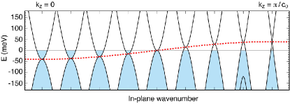
In three-dimensional graphite, however, it is known that the band touching points of the different subbands are not perfectly aligned but disperse along the energy axis as illustrated in Fig. 1.Koshino and Ando (2009) This is actually the origin of the semimetallic property of graphite, where an electron pocket and a hole pocket coexist at the Fermi energy. Dresselhaus and Dresselhaus (2002) The relative energy shift of the band touching point is characterized by the -parameter which is not captured in the minimal band model, and has a magnitude estimated to be about meV for graphite. Dresselhaus and Dresselhaus (2002) If in few-layer graphenes is of a similar magnitude as in graphite, we naively expect that the gap formation would be simply obstructed, since the energy gaps in the individual subbands are masked by the relative shift of the band center. Otherwise, there would have be some special mechanism that enables the spectral gap to overcome the semimetallic band overlapping.
In this paper, we explore the electronic ground states of Bernal-stacked multilayer graphenes from bilayer to 8-layer, using the Hartree-Fock mean-field approximation and the full-parameter band model. We find that a small of about 10 meV completely changes the nature of the insulating ground state, where the system takes a different strategy to have a spectral gap under the band overlapping. In 4-layer graphene, specifically, the ground state takes a staggered phase (odd parity) at , while introducing a finite stabilizes a different state with even parity, where the electrons are attracted to the top layer and the bottom layer, and the energy gap opens at the crossing point of overlapping electron and hole subbands. The even phase and odd staggered phase are topologically distinct insulating states with different Chern numbers. Multilayers with more than 5 layers in the presence of also exhibit similar ground states with the potential minima at the outermost layers, although the gap opening for the whole spectrum is generally harder than in 4-layer because of a larger number of energy bands overlapping at the Fermi energy. In odd-layer graphenes, the presence of minor band parameters (such as ) assists in band-gap opening for the monolayer-like linear band, which tends to blur the even-odd effect predicted in the minimal model.
The paper is organized as follows. We introduce the effective mass band model and the mean field treatment in Sec. II and III, respectively. In Sec. IV, we show the calculated results for the minimal band model neglecting all the extra band parameters including , where the staggered phase is the ground state in any layers. In Sec. V, we present the calculated results of the full parameter model, and discuss about the -stabilized even parity phase.
II Effective mass model
We describe the electronic properties of Bernal-stacked multilayer graphene using a Slonczewski-Weiss-McClure model of graphite Dresselhaus and Dresselhaus (2002). The low energy spectrum is given by states in the vicinity of the point in the Brillouin zone, where is the valley index. We define and as Bloch functions at the point, corresponding to the and sublattices of layer , respectively, where . In the basis of ; ; ; , the one-body Hamiltonian of multilayer graphene Guinea et al. (2007); Partoens and Peeters (2006); Koshino and Ando (2007, 2008) in the vicinity of the valley is
| (1) |
with
| (2) | |||
| (3) | |||
| (4) |
Here and . The diagonal blocks and are intralayer Hamiltonians for odd layer and even layers, respectively. Also, is the band velocity of monolayer graphene where is the nearest-neighbor intralayer hopping and is the lattice constant. The off-diagonal matrix describes the nearest-neighbor interlayer interaction, where is the vertical hopping between the dimer sites (those which lie directly above or below a site in an adjacent layer), and the velocity parameters and are related to the oblique hopping parameters and by . Matrices and describe coupling between next-nearest neighboring layers, and they only exist for . Parameters and couple a pair of non-dimer sites and a pair of dimer sites, respectively. Parameter represents the energy difference between dimer sites and non-dimer sites. It is related to the graphite band parameters as . In the following, we adopt parameter valuesDresselhaus and Dresselhaus (2002) eV, eV, eV, eV, eV and eV.
For comparison, we also perform the same analysis using the minimal model, where only two parameters and are retained in the band Hamiltonian above. The Hamiltonian matrix is then given by
| (5) |
with
| (6) |
III Mean-field theory
We include the electron-electron interaction in the mean-field approximation. The total Hamiltonian is written as with
| (7) | |||
| (8) |
where is the Bloch wavenumber measured from points, represents the sublattice degree of freedom, is the combined index for spin () and valley (), and and are the electron creation and annihilation operators, respectively. is the non-interacting band Hamiltonian where is the matrix element of Eq. (1). is the interaction part, where the first term and second term are the Hartree and exchange potentials, respectively. They are defined as
| (9) | |||
| (10) | |||
| (11) |
Here is the system area, and
| (12) |
is the two-dimensional Fourier transform of the Coulomb potential, and is the out-of-plane position of sublattice . Here is the dielectric constant in the interlayer spaces without the screening effect of -band electrons, which depends on the environment (e.g., substrate). The summation in is taken within the cutoff circle . Here we take eV, which is large enough to achieve convergence for moderate electron-electron interaction as considered below. In Eq. (10), represents the density of the positive background charge in the system. In the following, we consider the charge neutral case so that is determined by . Then Eq. (9) is reduced to
| (13) |
The label takes four different configurations . Here we neglect the exchange interaction between , which corresponds to with large momentum , and then can be treated just as a pseudo-spin label .
The strength of the electron-electron interaction is characterized by the effective fine structure constant for graphene,
| (14) |
As a typical value, for example, gives . In the simulation, however, should be effectively smaller than the bare value, considering that the Hartree-Fock approximation generally overestimates the exchange interaction. For bilayer graphene, is supposed to be of the order of 0.1 for a quantitative agreement with experiment. Jung et al. (2011) In the present study, we treat as a parameter in the range of .
We obtain the ground state by numerically solving the above equations. We start with an initial state with some particular configurations for the Hartree potential and exchange potential , and obtain the band structure and eigenfunctions by diagonalizing the Hamiltonian matrix. Then we calculate the next generation of and using Eqs. (9)-(11) with the expectation values estimated using the obtained eigenfunctions. Using new potential terms, we again calculate new eigenfunctions, and iterate the process until the potential terms converge. We confirm that the final state at convergence does not depend on the choice of the initial state. It sometimes branches into different solutions depending on the initial states, and then we determine the real ground state by comparing the total energy of the electronic system.
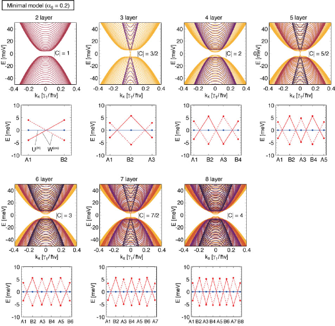
IV Minimal model
Figure 2 shows the band structures for the minimal band model from 2-layer to 8-layer graphenes with . The bottom panels plot the Hartree potential and the diagonal terms of the exchange potential at the valley center, , at non-dimer sites on successive layers . For , the constant term is subtracted so that its mean value is zero. The solid and dotted lines in represent different pseudospins, say, and , respectively. In all the multilayers studied here, we observe that the ground state takes a staggered arrangement as previously predicted Grushina et al. (2015); Yoon et al. (2017), where alternates its sign layer by layer. in and in are the positive and negative reversals of each other, and therefore the charge modulation exactly cancels in total, resulting in no cost for the Hartree potential. of a single species has an odd parity in space inversion, and it is a natural extension of the bilayer’s ground state breaking inversion symmetry.
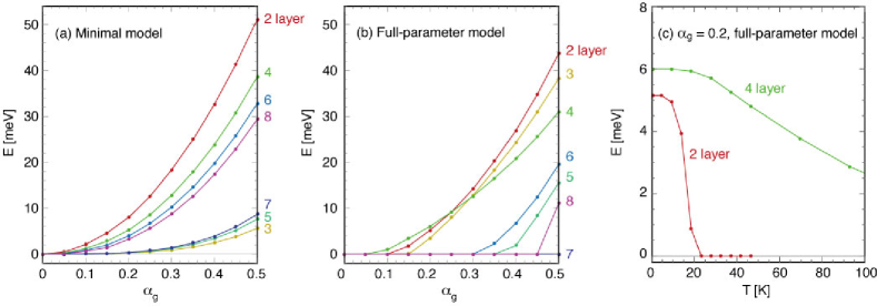
The low-energy spectrum of multilayer graphene is composed of pairs of electron and hole bands of the various band masses, and the monolayer-like linear (i.e. zero mass) band appears only in odd-layer graphenes Guinea et al. (2007); Partoens and Peeters (2006); Koshino and Ando (2007, 2008). In the minimal model, all the subbands are aligned on the energy axis, i.e. the conduction and valence bands exactly touch at zero energy in the absence of the electron-electron interaction. For , we observe that a noticeable energy gap opens in even-layer graphene, while it is nearly vanishing in odd-layer graphene due to only a tiny gap in the linear band. We see a general tendency that the gap width becomes greater in a subband with a heavier mass and it is the smallest in the linear (zero mass) band. Figure 3(a) plots the band gap in the total spectrum as a function of . In the even-layer graphenes, the gap increases approximately , and the gap is smaller for thicker multilayers. The energy gaps in odd-layer graphenes increase much more slowly than in even-layer graphenes, and they become significant only for . We can show that, in all the multilayers, the profiles of the Hartree and exchange potential do not depend on , except for the energy scale.
The staggered potential gives rise to a non-trivial topological property of the band structure. In Fig. 2, an integer appended near the energy gap in each panel indicates the absolute value of the total Chern number summed over all the valence bands in a single pseudo-spin branch. The Chern number corresponds to the quantized Hall conductivity in units of contributed from the pseudo-spin. We see that -layer graphene has in all cases, so that the state in each pseudo-spin sector is a Chern insulator. The sign of the Chern number depends on the sign of the staggered potential (i.e., the solid line or dashed line in Fig. 2) and also on the chirality ( or ). Specifically, if the signs of at take the values (where ) for valley, then . The total Hall conductivity is given by the summation of over all the spin and valley sectors. We can have various states such as the quantum Hall state and the quantum spin (or valley) Hall state depending on how to assign to valleys, McCann and Koshino (2013) while they are not energetically distinguishable in the present calculation which treats the pseudo-spins as independent sectors.
V Full-parameter model
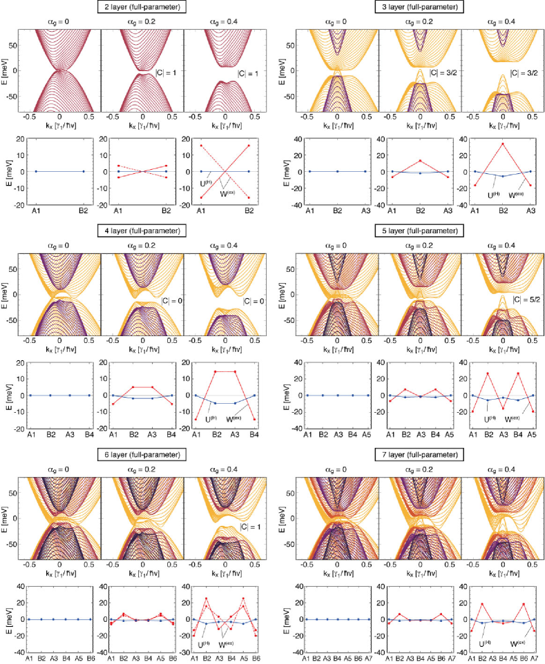
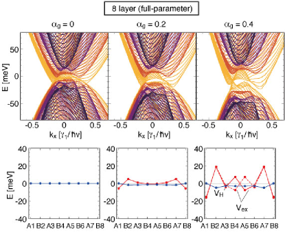
The nature of the ground state changes drastically when additional band parameters are included. Figure 4 presents the band structures for the full parameter models of 2 layer to 7 layer with and 0.4. The panel of 8-layer is shown in Fig. 5 . In bilayer, the tendency is almost unchanged from the minimal model. In 4-layer, however, the ground state takes an inversion-symmetric configuration with even parity, in a striking contrast to the staggered phase observed in the minimal model. Also it takes the identical configuration regardless of the pseudo-spins. We observe similar ground states in other multilayers for , where takes a low value at the outermost layers, and its highest value at the second outer-most layers, independently of the pseudo-spin.
The appearance of a different type of ground state originates from the presence of the next-nearest layer hopping parameter which only exists for . In the full-parameter model, the band edge of electron and hole bands are not aligned in energy in the absence of the electron-electron interaction (i.e. the conduction and valence bands do not touch exactly at zero energy) unlike in the minimal model. This is due to the parameter, which is responsible for the semi-metallic nature of graphite where the electron Fermi surface and the hole Fermi surface coexist. Dresselhaus and Dresselhaus (2002) Therefore, opening a small gap at the band touching point of each electron-hole pair does not result in a gap opening of the total spectrum, so that the system needs to adopt a different strategy in order to open a gap. Actually, we can show that the outermost attractive potential observed here partially cancels the effect of and aligns the band centers (See, appendix). This assists the opening of an energy gap by reducing the band overlapping at the Fermi energy.
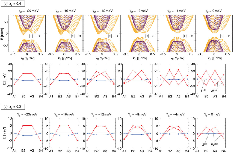
In Fig. 6(a), we present the band structure and the mean-field potential in the full-parameter model for 4-layer graphene with , in which the parameter is reduced from its value in graphite ( meV) down to zero with all other parameters unchanged. We see that the ground state gradually changes from the even-parity phase to the odd-parity, staggered phase as decreases. An interesting observation is that the total Chern number below the gap, , is zero in the even phase while it is 2 in the staggered phase, so there is a topological phase transition at some stage as decreases. vanishes in the even phase, because the surviving inversion symmetry and time-reversal symmetry requires a vanishing Berry phase everywhere except at the band-degeneracy point. Haldane (2004); Koshino (2013) Experimentally, the non-zero Hall conductivity in a single pseudo-spin sector causes a valley or spin Hall effect, McCann and Koshino (2013) so that the even and odd phases can be distinguished by measuring it. In Fig. 6(b), we show similar plots of the mean-field potential for weaker interaction, . We observe that the even phase survives down to smaller compared to , suggesting that the -stabilized even phase is more stable for weaker interactions.
Generally, the band touching points of the intrinsic even-layer graphene are protected by spatial inversion symmetry and time-reversal symmetry. Mañes et al. (2007); Koshino (2013) More specifically, the coexistence of the two symmetries requires the vanishing of the Berry curvature at any non-degenerate band states, and this immediately concludes that a band touching point with non-trivial Berry phase cannot be split, because otherwise non-zero Berry curvature arises where the degeneracy is lifted. In 4-layer graphene, the band gap opening in the even-parity state may appear to contradict with this fact, but, there, band touching actually remains between the first and the second bands and also between the third and the fourth bands (out of the four low-energy bands) so a band gap can open at the center without breaking these degenerate points. In bilayer graphene, on the other hand, there are only two bands at the charge neutral point, so that inversion-symmetry breaking is the only way to open a gap, as actually observed in Fig. 4. The 6-layer graphene has a similar situation to bilayer where the six low-lying bands touch in pairs of (1,2), (3,4) and (5,6) under the inversion symmetry, and the middle pair (3,4) prevents a gap opening at the charge neutral point. In the numerical calculation shown in Fig. 4, we actually see that the gapped state at slightly breaks the inversion symmetry (of in each single species) on top of the even-parity feature. The above argument for band touching does not apply to odd-layer graphenes where the inversion symmetry is intrinsically absent.
The energy gap width as a function of is shown in Fig. 3(b). For , which is supposed to match the real experimental situation, the energy gap is the largest in 4-layer, in which it is even bigger than in bilayer. Thicker graphenes () require a large interaction to have a gap because of the severely overlapping energy bands (in the absence of interactions). However, 3-layer graphene is atypical because its gap is much more significant for than in the minimal model. In the full parameter model at , the additional band parameters , and cause the monolayer and bilayer-like bands in 3-layer to overlap each other (hence there is no overall band gap), but, when viewed separately, the monolayer bands are gapped and the bilayer-like bands are gapped, too. This then assists the gap opening of the whole spectrum for .
Figure 3(c) shows the temperature dependence of the energy gap of 2- and 4-layer graphenes at . It shows that the gap in 4-layer remains up to much higher temperature than in bilayer, even though at zero temperature they are of a similar order. The critical temperature for the gap closing is determined by the characteristic energy scale of the band structure contributing to the total energy minimization. In the bilayer, the change of the energy band due to the electron-electron interaction only takes place near the gap within the energy scale about a few meV at as seen in Fig. 4. In 4-layer, on the other hand, the band structure near already has some complex structure in the energy range about 20 meV, and they all contribute to the charge transfer and the total energy reduction. To smear out the gap, we need a temperature to match this energy scale, and it becomes much greater than in bilayer.
VI Conclusion
We studied the electronic band structure in Bernal-stacked multilayer graphenes under the electron-electron interaction, using the mean-field theory and the band model fully including band parameters. We demonstrated that the ground state is governed by the semimetallic parameter , where the previously-conjectured staggered state yields to an even-parity state in the presence of , where the outermost layers have the lowest potential energy. We also found that the staggered phase and the even-parity phase have different Chern numbers and they can be distinguished by valley / spin Hall conductivity measurements.
In the ground state calculation, we treat and the interaction strength as variable parameters, and quantitatively estimate the energy gap width in changing parameters. Experimentally, the insulating gap was observed not only in Bernal-stacked bilayer Freitag et al. (2012); Velasco Jr et al. (2012); Bao et al. (2012); Veligura et al. (2012); McCann and Koshino (2013), but also in 4-layerGrushina et al. (2015), 6-layer and 8-layer graphenesNam et al. (2016). According to Fig. 3, the opening of a gap for 6 and 8-layers within the full-parameter model requires a fairly high interaction , but such a high interaction would result in bilayer’s gap being more than 30 meV, which is inconsistent with experiment. This suggests that the value of in few-layer graphenes may be actually lower than in graphite, and the reality could be somewhere between Figs. 3(a) and (b). While the reason for suppression of is unclear, it is possible, for example, that the optimum lattice structure of a few-layer device takes a different interlayer spacing from graphite’s, and that modifies .Nam et al. (2016) The is a small band parameter corresponding to the next-nearest neighbor interlayer hopping, and it should be sensitive to the interlayer spacing. Unknown values of band parameters including should be clarified by detailed spectroscopic measurements for few-layer graphenes. It is also conceivable that other factors, such as the effect of disorder or of interactions beyond mean-field theory, would be significant for further quantitative arguments. The study of these issues is left as an open question.
Acknowledgements.
The authors thank Alberto F. Morpurgo and Kazuhiko Kuroki for helpful discussions. This work was supported by JSPS KAKENHI Grant Numbers JP15K21722, JP25107001 and JP25107005.References
- McCann and Koshino (2013) E. McCann and M. Koshino, Rep. Prog. Phys. 76, 056503 (2013).
- McCann and Fal’ko (2006) E. McCann and V. I. Fal’ko, Phys. Rev. Lett. 96, 086805 (2006).
- Koshino and Ando (2006) M. Koshino and T. Ando, Phys. Rev. B 73, 245403 (2006).
- Guinea et al. (2006) F. Guinea, A. Castro Neto, and N. Peres, Phys. Rev. B 73, 245426 (2006).
- Freitag et al. (2012) F. Freitag, J. Trbovic, M. Weiss, and C. Schönenberger, Phys. Rev. Lett. 108, 076602 (2012).
- Velasco Jr et al. (2012) J. Velasco Jr, L. Jing, W. Bao, Y. Lee, P. Kratz, V. Aji, M. Bockrath, C. Lau, C. Varma, R. Stillwell, et al., Nat. Nanotech. 7, 156 (2012).
- Bao et al. (2012) W. Bao, J. Velasco, F. Zhang, L. Jing, B. Standley, D. Smirnov, M. Bockrath, A. H. MacDonald, and C. N. Lau, PNAS 109, 10802 (2012).
- Veligura et al. (2012) A. Veligura, H. J. van Elferen, N. Tombros, J. C. Maan, U. Zeitler, and B. J. van Wees, Phys. Rev. B 85, 155412 (2012).
- Nilsson et al. (2006) J. Nilsson, A. H. Castro Neto, N. M. R. Peres, and F. Guinea, Phys. Rev. B 73, 214418 (2006).
- Min et al. (2008) H. Min, G. Borghi, M. Polini, and A. H. MacDonald, Phys. Rev. B 77, 041407 (2008).
- Vafek (2010) O. Vafek, Phys. Rev. B 82, 205106 (2010).
- Zhang et al. (2010) F. Zhang, H. Min, M. Polini, and A. H. MacDonald, Phys. Rev. B 81, 041402 (2010).
- Nandkishore and Levitov (2010) R. Nandkishore and L. Levitov, Phys. Rev. B 82, 115124 (2010).
- Zhang et al. (2011) F. Zhang, J. Jung, G. A. Fiete, Q. Niu, and A. H. MacDonald, Phys. Rev. Lett. 106, 156801 (2011).
- Jung et al. (2011) J. Jung, F. Zhang, and A. H. MacDonald, Phys. Rev. B 83, 115408 (2011).
- Kharitonov (2012) M. Kharitonov, Phys. Rev. B 86, 195435 (2012).
- Grushina et al. (2015) A. L. Grushina, D.-K. Ki, M. Koshino, A. A. Nicolet, C. Faugeras, E. McCann, M. Potemski, and A. F. Morpurgo, Nat. Commun. 6 (2015).
- Nam et al. (2016) Y. Nam, D.-K. Ki, M. Koshino, E. McCann, and A. F. Morpurgo, 2D Mater. 3, 045014 (2016).
- Partoens and Peeters (2006) B. Partoens and F. Peeters, Phys. Rev. B 74, 075404 (2006).
- Koshino and Ando (2007) M. Koshino and T. Ando, Phys. Rev. B 76, 085425 (2007).
- Koshino and Ando (2008) M. Koshino and T. Ando, Phys. Rev. B 77, 115313 (2008).
- Koshino and Ando (2009) M. Koshino and T. Ando, Solid State Commun. 149, 1123 (2009).
- Yoon et al. (2017) C. Yoon, Y. Jang, J. Jung, and H. Min, 2D Mater. 4, 021025 (2017).
- Dresselhaus and Dresselhaus (2002) M. S. Dresselhaus and G. Dresselhaus, Adv. Phys. 51, 1 (2002).
- Guinea et al. (2007) F. Guinea, A. Castro Neto, and N. Peres, Solid state communications 143, 116 (2007).
- Haldane (2004) F. Haldane, Phys. Rev. Lett. 93, 206602 (2004).
- Koshino (2013) M. Koshino, Phys. Rev. B 88, 115409 (2013).
- Mañes et al. (2007) J. L. Mañes, F. Guinea, and M. A. Vozmediano, Phys. Rev. B 75, 155424 (2007).