Universal experimental test for the role of free charge carriers in thermal Casimir effect within a micrometer separation range
Abstract
We propose a universal experiment to measure the differential Casimir force between a Au-coated sphere and two halves of a structured plate covered with a P-doped Si overlayer. The concentration of free charge carriers in the overlayer is chosen slightly below the critical one, for which the phase transition from dielectric to metal occurs. One half of the structured plate is insulating, while its second half is made of gold. For the former we consider two different structures, one consisting of bulk high-resistivity Si and the other of a layer of SiO2 followed by bulk high-resistivity Si. The differential Casimir force is computed within the Lifshitz theory using four approaches that have been proposed in the literature to account for the role of free charge carriers in metallic and dielectric materials interacting with quantum fluctuations. According to these approaches, Au at low frequencies is described by either the Drude or the plasma model, whereas the free charge carriers in dielectric materials at room temperature are either taken into account or disregarded. It is shown that the values of differential Casimir forces, computed in the micrometer separation range using these four approaches, are widely distinct from each other and can be easily discriminated experimentally. It is shown that for all approaches the thermal component of the differential Casimir force is sufficiently large for direct observation. The possible errors and uncertainties in the proposed experiment are estimated and its importance for the theory of quantum fluctuations is discussed.
pacs:
12.20.Ds, 42.50.Ct ,42.50.Lc,I Introduction
During the last two decades the Casimir force 1 acting between two closely spaced uncharged material surfaces attracted much experimental and theoretical attention due to the diverse roles it plays in both fundamental and applied physics (see the monograph 2 and the reviews 3 ; 4 ; 5 ). The Casimir effect is an entirely quantum and (at separations between surfaces exceeding two or three nanometers) relativistic phenomenon. In the nonrelativistic region the Casimir force is commonly known as van der Waals force 6 . The Casimir effect is caused by the zero-point and thermal fluctuations of the electromagnetic field. Although Casimir 1 calculated the force acting between two ideal metal planes, Lifshitz 7 developed a general theory of van der Waals and Casimir forces between two parallel material plates described by the respective frequency-dependent dielectric permittivities. In recent years this theory has been generalized to the case of arbitrarily shaped interacting bodies 5 .
In 2000 it has been shown that the Lifshitz theory leads to widely different predictions for the thermal Casimir force between metallic test bodies depending on whether the low-frequency dielectric response of metals is described by either the lossy Drude 8 or lossless plasma 9 model. Later it was demonstrated that if the Drude model is used the Casimir entropy calculated within the Lifshitz theory does not satisfy the third law of thermodynamics (the Nernst heat theorem) for both nonmagnetic 10 ; 11 ; 12 ; 13 and magnetic 14 metals with perfect crystal lattices. If instead the plasma model is used, the Lifshitz theory was found to be in perfect agreement with the Nernst theorem 10 ; 11 ; 12 ; 13 ; 14 . By contrast, in the limiting case of large separations between metallic plates, for which classical statistical physics should be applicable, a first principle computation based on a microscopic model was shown in Ref. 15 to reproduce the Casimir force predicted by the Lifshitz theory combined with the Drude model. The Drude model has been later shown to satisfy the Bohr-van Leeuwen theorem of classical statistical physics, which is, however, violated if the plasma model is used to calculate the Casimir force at large separations 16 . It was shown also that the difference in theoretical predictions of the Drude and plasma models could be attributed to the magnetic interaction among fluctuating Foucault currents 16a ; 16b ; 16c .
In two series of precise experiments on measuring the Casimir interaction between metals by means of a micromechanical oscillator 17 ; 18 ; 19 ; 20 and an atomic force microscope 21 ; 22 ; 23 , theoretical predictions of the Lifshitz theory using the Drude model dielectric response at low frequencies have been excluded by the measurement data at up to 99% confidence level. The theoretical predictions obtained using the plasma model turned out to be in agreement with the data at a 90% confidence level 24 . All these experiments were performed at separations below one micrometer, where the difference between the theoretical predictions using the Drude and plasma models does not exceed a few percent. The only experiment performed at separations up to m was interpreted to be in agreement with theoretical predictions of the Lifshitz theory combined with the Drude model 25 . It was noted, however, that in Ref. 25 the Casimir force was extracted by means of a fitting procedure from up to an order of magnitude larger measured force, supposedly originating from electrostatic patches and influenced by imperfections, which are unavoidably present on the surfaces of lenses with centimeter-size radii 26 ; 27 . Thus, the majority of experiments on measuring the Casimir force do confirm the lossless plasma model. Since the relaxation of free electrons in metals at low frequencies is a much studied fact, this situation is regarded in the literature as the Casimir puzzle.
The Casimir force acting on dielectric bodies also presents a puzzle. The problem is that the measurement data of all precise experiments with dielectric surfaces are in agreement with theoretical predictions of the Lifshitz theory only provided that the contribution of free charge carriers in the dielectric response (dc conductivity) is omitted in computations 28 ; 29 ; 30 ; 31 . If the dc conductivity of dielectric bodies is taken into account, the theoretical predictions of the Lifshitz theory are excluded by the measurement data 28 ; 29 ; 30 ; 31 ; 32 . Similar to the role of relaxation of free charge carriers in metallic bodies, the influence of the dc conductivity in the Casimir force on dielectric bodies is limited to just a few percent of the measured signal. Theoretically it was proven that the Lifshitz theory with included dc conductivity of dielectric materials violates the Nernst heat theorem, while an agreement with this theorem is restored if the dc conductivity is omitted 33 ; 34 ; 35 ; 36 . This makes us again to disregard a real physical phenomenon (here, the conductivity of a dielectric material at nonzero temperature) to achieve agreement with both experimental data and the third law of thermodynamics.
It is worth noting that the impact of both relaxation phenomena in metals and of the dc conductivity in dielectrics on the Casimir force at separations below m is always relatively small. Then one may hope that by a proper account of some background effects due to, e.g., electrostatic patches 37 or surface roughness 3 ; 37aa one could bring predictions of the literally understood Lifshitz theory in agreement with the data. To invstigate this possibility, Ref. 37a proposed to measure the Casimir force between two aligned sinusoidally corrugated Ni surfaces, one of which is coated with a thin opaque Au layer having a flat surface. According to the results obtained, the phase-dependent modulation of the Casimir force for submicron separations, predicted by the Drude model, is several orders of magnitude larger than that predicted by the plasma model. An experiment based on this principle 38 has already measured the differential force between Au- or Ni-coated spheres and Au and Ni sectors of a structured disc covered with an Au overlayer at separations of a few hundreds nanometers. The measurement data unequivocally ruled out the Drude model and were found to be in good agreement with the plasma model 38 . This experiment is immune to electrostatic forces caused by patch potentials similarly to isoelectronic differential force measurements searching for Yukawa-type corrections to Newton’s gravitational law 39 ; 40 . It is interesting to point out that the Casimir free energies and pressures of thin metallic films computed using the Drude and plasma models have also been found to differ by up to a factor of several thousands 41 ; 42 ; 43 . It is found again that the Nernst heat theorem is violated if the Drude model is used in computations 44 .
In view of the above considerations it would be clearly desirable to perform an experimental test for the role of free charge carriers in the Casimir force in the micrometer separation range where thermal effects are most pronounced. Differential force measurements of this sort have been proposed in Refs. 44a ; 44b for both nonmagnetic and magnetic metallic test bodies. The setup considered in Refs. 44a ; 44b involved a structured plate, one half of which was made of a metal (Au or Ni) and the other half of high-resistivity Si. The structured plate was covered with a plane-parallel overlayer made of B-doped Si plate in the metallic state with a thickness of 100 nm. This setup allows for a measurable differential force between a metal-coated sphere and the two halves of a sample, which is of a quite different magnitude depending on whether the metal is described by either the Drude or the plasma model. The test of Refs. 44a ; 44b is not sensitive, however, to the dc conductivity of high-resistivity Si.
In this paper, we propose a universal test for the role of free charge carriers in the Casimir force in the micrometer range of separations. It follows the main idea of Refs. 44a ; 44b , i.e., it suggests to measure the differential Casimir force between a Au-coated sphere and the high-resistivity Si and Au halves of a structured plate. The main difference is, however, that we now consider a semitransparent overlayer made of P-doped Si with a concentration of free charge carriers which is only slightly smaller than the critical concentration for which the dielectric-to-metal phase transition occurs. This means that the used overlayer is in a dielectric state although it preserves all experimental advantages of having rather high electronic conductivity.
We calculate the differential Casimir force in the configuration including both metallic and dielectric materials using the following four theoretical approaches: in the first one Au at low frequencies is described by the plasma model and the conductivity of Si is disregarded; in the second approach Au at low frequencies is described by the plasma model but the conductivity of Si is taken into account; in the third one Au at low frequencies is described by the Drude model but the conductivity of Si is disregarded; finally, in the fourth approach the low-frequency dielectric response of Au is described by the Drude model and the conductivity of Si is taken into account. We compute the differential Casimir force using these four approaches and show that in all of them the obtained results are widely different in the micrometer separation range and can be easily discriminated using the already available experimental setup. It is shown that the proposed experiment allows for a precise measurement of the thermal effect in the Casimir force. We also propose a modified structure of the plate by adding a layer of SiO2, which offers some advantages for the process of plate preparation and further increases the relative differences between theoretical predictions made by the four approaches. Computations of the differential Casimir forces are performed using the tabulated optical data of all involved materials over the frequency ranges for which they are available. The estimation of both theoretical and experimental errors and uncertainties in the proposed experiment demonstrates its feasibility.
The structure of the paper is as follows. In Sec. II the principle scheme of the proposed experiment is outlined and the general formalism is presented. Section III contains the results of numerical computations of the differential Casimir force within the four theoretical approaches. Section IV presents the modified experimental scheme and more detailed computational results for the differential force. In Sec. V all errors and uncertainties are estimated. In Sec. VI the reader will find our conclusions and discussion.
II Principal experimental scheme and general formalism
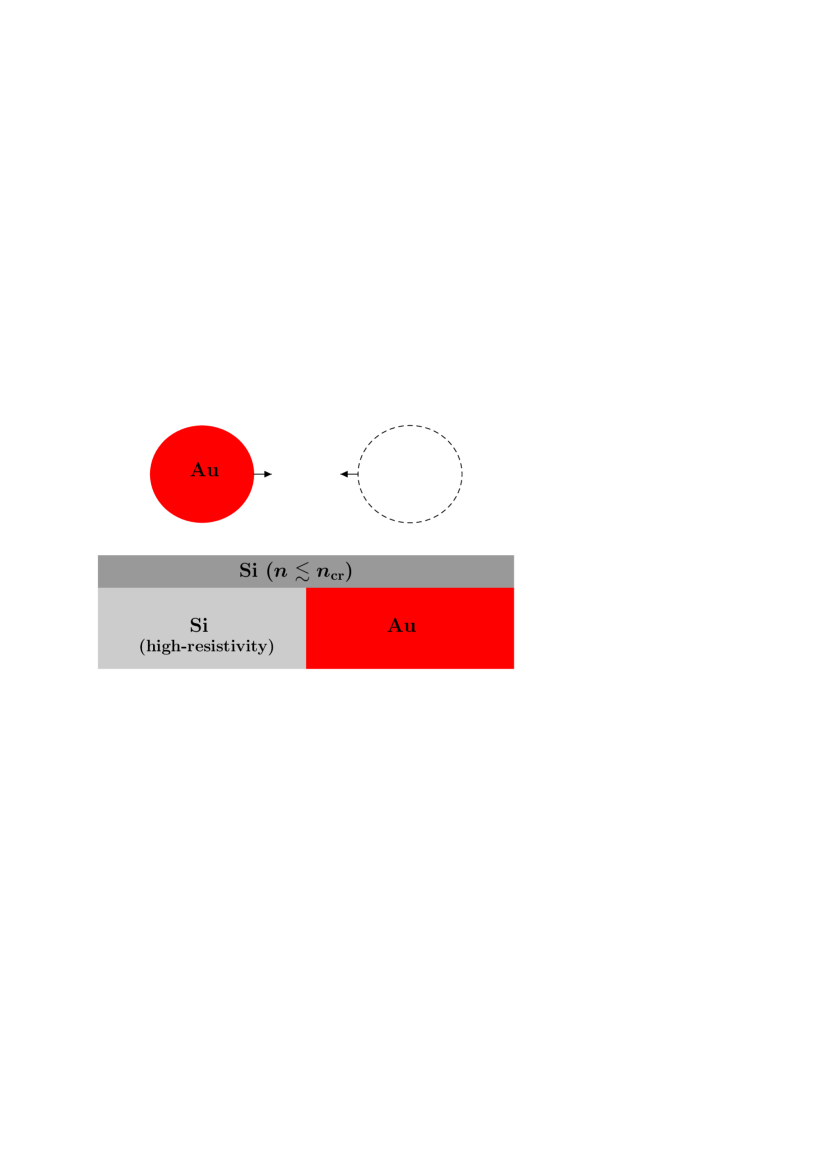
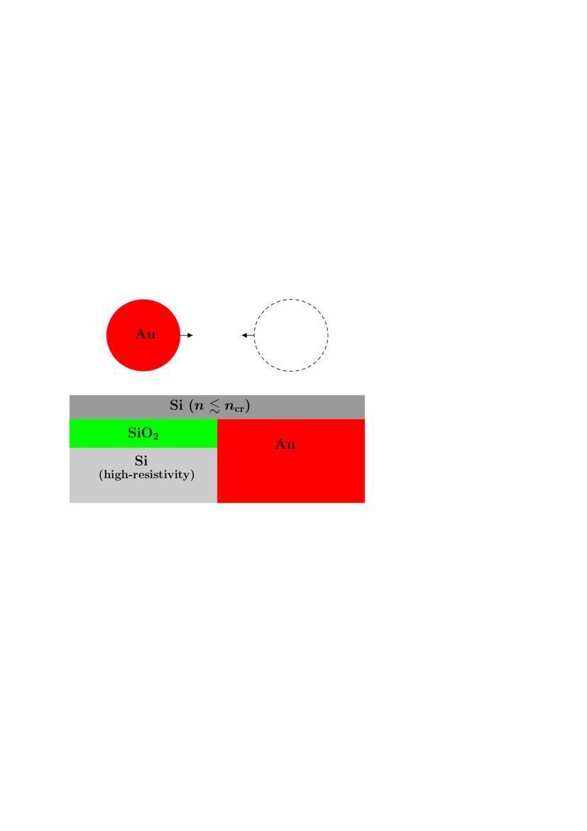
We consider the configuration of a Au-coated sapphire sphere with radius m in vacuum, at a separation from a structured plate at room temperature K. The thickness of the Au coating is assumed to exceed 100 nm, in such a way that it is legitimate to consider the sphere as if it were made entirely of gold, for the sake of computing the Casimir force. The structured plate consists of an overlayer made of P-doped Si of thickness nm covering two sections one of which is made of high-resistivity Si, while the other is made of Au (see Fig. 1). The thickness of both sections is large enough to consider them as two semispaces. We consider an overlayer with rather high electronic conductivity corresponding to the density of free charge carriers . This density is, however, slightly smaller than the critical density at which the dielectric-to-metal phase transition occurs 45 . Thus, both the overlayer and the underlying left section of the plate are made of dielectric materials although with quite different densities of free charge carriers.
We denote the materials of the sphere, of the overlayer, and of the left section of the plate as 1, 2, and 3, respectively. Then the material of the right section of the plate is also denoted as 1. We denote the vacuum gap as material 0. The respective dielectric permittivities at the pure imaginary Matsubara frequencies are
| (1) |
Here, , with and being the Boltzmann constant are the Matsubara frequencies, and are the dimensionless Matsubara frequencies. For a vacuum gap we have .
In the proposed experiment the sphere moves back and forth with sufficiently high frequency at some fixed separation from the plate. In this case not the Casimir forces and among the Au sphere and the left and right sections of the plate but only the difference between them is measured 38 ; 39 ; 40 :
| (2) |
This measurement should be repeated at different separations. Note that and are the forces acting when the sphere bottom is above some points deep in the left and right halves of the plate, respectively. Because of this, one can neglect the effect of sharp boundary between the left and right halves of the plate and consider each of them as infinitely large 44b .
Using the proximity force approximation 2 , which was recently shown to be sufficiently exact under the condition 46 ; 47 ; 48 , and the Lifshitz formula 2 ; 7 , the differential force (2) can be calculated by the following equation:
| (3) | |||
where the prime on the summation sign denotes that the term is taken with weight 1/2. Here, is the dimensionless variable connected with the projection of the wave vector onto the plane of the plate, , by
| (4) |
The summation in is made over the two independent polarizations of the electromagnetic field, transverse magnetic () and transverse electric (). The reflection coefficients on the structured plate covered with the overlayer are expressed as
| (5) |
where . Finally, the reflection coefficients on the boundary surfaces between two different materials are given by the familiar Fresnel formulas taken at the imaginary Matsubara frequencies:
| (6) |
where , and (2,3).
The contribution to Eq. (3) at zero Matsubara frequency requires special attention because the problems discussed in Sec. I are connected with different treatments of this contribution. The point is that the optical data for the complex index of refraction of all materials are available only for sufficiently large frequencies. Therefore, at low frequencies the available data should be supplemented with some theoretical model. Taking into account the relaxation properties of electrons in metals, the dielectric permittivities of our material 1 (Au) at the Matsubara frequencies can be represented in the form
| (7) |
Here, and are, respectively, the dimensionless plasma frequency and relaxation parameter of Au connected with the dimensional ones by
| (8) |
and is a contribution of the core (bound) electrons to the dielectric permittivity determined by the optical data. The upper index is used to underline that the permittivity (7) has the Drude form. Note that the relaxation parameter depends on temperature and goes to zero with vanishing by a power law. For metals with disregarded relaxation properties of free electrons the dielectric permittivity takes the plasma form
| (9) |
The plasma model is usually used in the region of infrared optics where .
For dielectric materials () with free charge carriers taken into account the dielectric permittivity at the Matsubara frequencies takes the form
| (10) |
where the dimensionless conductivity is connected with the dimensional one by
| (11) |
The conductivity of dielectrics is temperature-dependent. It vanishes exponentially fast when goes to zero. At room temperature it is customary to represent the frequency dependence of in terms of conventional Drude parameters, i.e., as
| (12) |
If the free charge carriers in dielectric materials are disregarded, it holds
| (13) |
For our dielectric materials with (P-doped Si) and (high-resistivity Si)
| (14) |
although and are significantly different. Note also that for both metals and dielectrics when .
At first, we assume that the free charge carriers in both dielectric materials (i.e., in the overlayer made of doped Si and in the plate section of high-resistivity Si) are disregarded. Then, at Eqs. (13) and (14) hold. In this case, from the first line of Eq. (6) one obtains and from Eq. (5) we have
| (15) |
Now, from the first line of Eq. (6), one can see that independently of whether Au is described by the Drude model of Eq. (7) or by the plasma model of Eq. (9). Then, Eq. (5) leads to
| (16) |
where is given by Eq. (15).
From the second line of Eq. (6) we have
| (17) |
Then, from Eq. (5) one obtains
| (18) |
As to the reflection coefficient , its value depends on whether Au is described by the Drude or the plasma model. If the Drude model (7) is used, the second line of Eq. (6) leads to and Eq. (5) results in
| (19) |
similar to Eq. (18). If, however, the plasma model (9) is used for Au, the second line of Eq. (6) leads to
| (20) |
and from Eq. (5) one obtains
| (21) |
Next, we assume an alternative assumption that the free charge carriers in dielectric materials are taken into account by Eq. (10). In this case and from Eq. (5) we have
| (22) |
Notice that the latter equation is valid irrespective of whether Au is described by the Drude or the plasma models. For the TE mode Eq. (17) is still valid leading to
| (23) |
The value of the coefficient depends on the model used for a description of Au. If the Drude model is used,
| (24) |
If, however, Au is described by the plasma model, one returns back to Eqs. (20) and (21), which preserve their validity when the free charge carriers in dielectric materials are taken into account.
From the above one can see that at zero Matsubara frequency the coinciding reflection coefficients with are obtained in the cases when the free charge carriers of the dielectric materials 2 and 3 are either disregarded or taken into account. In each case, however, the results for depend on the model used for a description of Au. Just the opposite situation holds for the coefficients calculated at . Here, the results do not depend on the model of a metal, but are different depending on whether or not the free charge carriers of dielectric materials are taken into account.
III Discrimination between different theoretical approaches
Now we perform numerical computations of the differential Casimir force (2) in the configuration of Sec. II by using Eqs. (3)–(5) and the explicit expressions for the reflection coefficients at zero Matsubara frequency provided in Eqs. (15), (16), (18), (19), (21)–(24) obtained in the framework of different theoretical approaches. The dielectric permittivities of Au and Si at the Matsubara frequencies were obtained using the tabulated optical data for the complex index of refraction 49 ; 50 and the Kramers-Kronig relation following Refs. 2 ; 3 . For Au the values of the plasma frequency rad/s and the relaxation parameter rad/s have been used.
For P-doped Si the chosen concentration of free electrons () corresponds to the plasma frequency
| (25) |
where the effective electron mass is . The chosen value of corresponds also to the resistivity cm 51 , i.e., s and conductivity . If one models the conductivity of P-doped Si at fixed K by means of the Drude model, this value of conductivity leads to the following relaxation parameter 52
| (26) |
Now we consider the material 3, i.e., high-resistivity Si whose conductivity is by about five orders of magnitude lower than that of our P-doped Si. If the free charge carriers in Si are disregarded, materials 2 and 3 become identical and their common dielectric permittivity is given by . Note, that for Si . Inclusion of free charge carriers for high-resistivity Si affects the dielectric permittivity only at the zero Matsubara frequency and results in nonzero dc conductivity. Now we take into account that according to Eqs. (18) and (23) the reflection coefficient takes the same value irrespective of whether one includes or neglects the contribution to the permittivity of free charge carriers in Si. On the contrary the value of the coefficient does depend on whether one includes or not the contribution of free charge carriers in the P-doped Si overlayer [see Eqs. (15) and (22)]. However, even in this case it does not depend on the conductivity properties of high-resistivity Si.
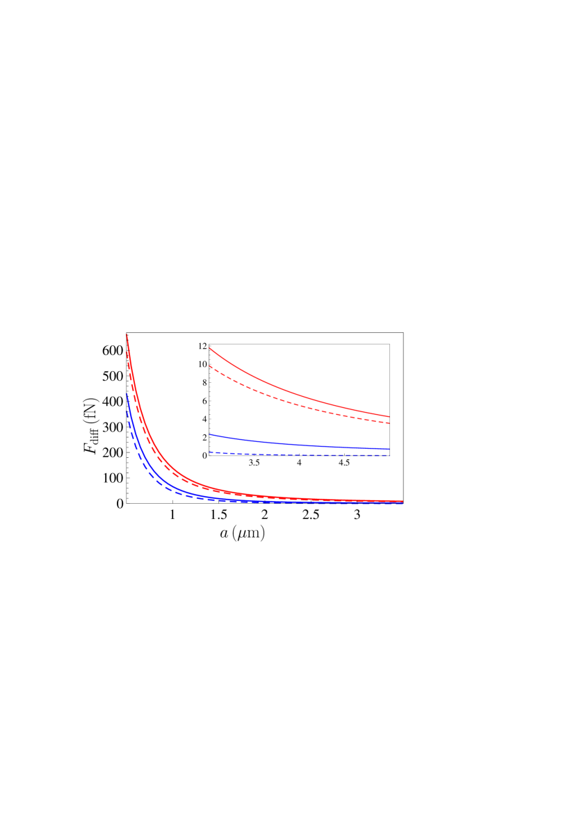
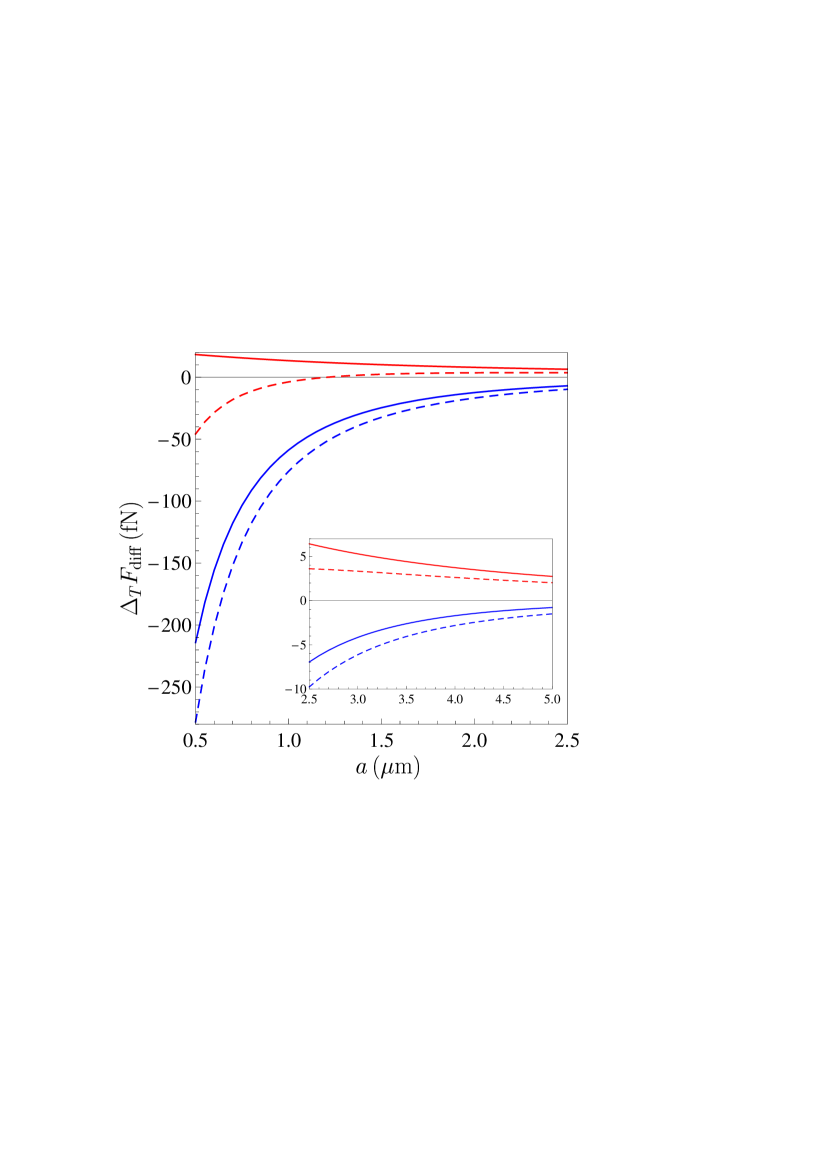
The results of the computations for the differential Casimir force (2) at K are presented in Fig. 2 as functions of separation in the range from 0.5 to m and, on an enlarged scale, in an inset in the range from 3 to m. The pair of top lines (solid and dashed) is computed using the plasma model (9) for Au. The free charge carriers in both the P-doped and high-resistivity Si are either disregarded according to Eq. (13) (the solid line) or taken into account according to Eq. (10) (the dashed line). In a similar way, the pair of solid and dashed bottom lines is computed using the Drude model (7) for Au. Here, the solid line is again computed by disregarding the free charge carriers in dielectric materials and the dashed line takes these charge carriers into account.
As it is seen in Fig. 2, the four theoretical approaches discussed in Sec. I lead to widely different predictions for the differential Casimir force. They can be easily discriminated experimentally keeping in mind that the sensitivity of difference force measurements of this type is equal to 1 fN 38 or even a fraction of 1 fN 40 . Thus, for m use of plasma model for Au results in fN and fN with disregarded and included free charge carriers, respectively, in both P-doped Si overlayer and high-resistivity Si (the top pair of lines). If Au is described by the Drude model and the free charge carriers are either disregarded or included one has fN or fN, respectively (the bottom pair of lines). It is seen that the four theoretical predictions are approximately 18, 54 and 18 fN apart, i.e., the force intervals between them far exceed the experimental sensitivity. Even for m we have fN and fN with disregarded and taken into account free charge carriers in Si materials, respectively, and fN and fN under the same assumptions about the free charge carriers. Here, the theoretical predictions are approximately 5, 16, and 4 fN apart, i.e., again can be experimentally discriminated (see Sec.V for additional information about errors and uncertainties in this experiment).
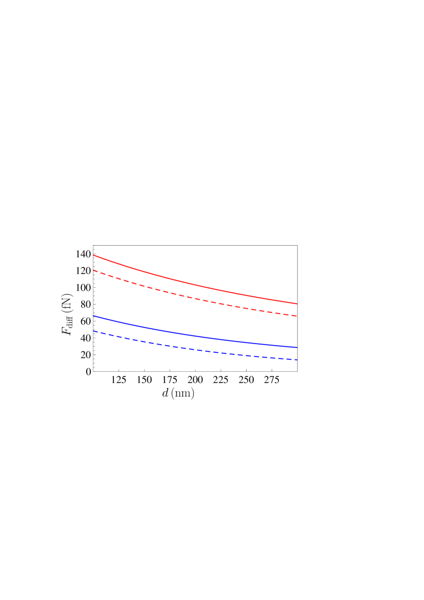
In the above computations, the P-doped Si overlayer of nm thickness has been used. It is interesting to determine the dependence of on . In Fig. 3 the computational results for the differential Casimir force at m, K are presented as a function of overlayer thickness using the four theoretical approaches described above (the top pair of the solid and dashed lines is computed using the plasma model for Au with disregarded and included free charge carriers in Si, respectively; the bottom pair of the solid and dashed lines is computed using the Drude model with either disregarded or included free charge carriers in Si). As it can be seen in Fig. 3, the differential Casimir force decreases monotonously with increasing , while the discrepancies between the theoretical predictions of the different models are almost independent on the thickness. This feature of the force makes a thicker overlayer (for instance, nm, see Sec. IV) preferable because in this case the relative error in the determination of becomes negligibly small and therefore it does not influence the value of . A more detailed analysis of theoretical errors is contained in Sec. V.
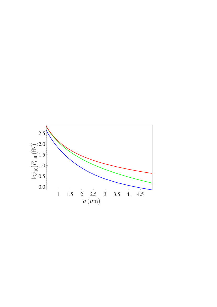
Now we show that the proposed experiment not only allows for an easy discrimination between the four theoretical approaches described above, but it can be used to measure the thermal effect in as well. First, we illustrate this statement for the case of Au described by either the Drude or the plasma model with disregarded free charge carriers in Si. In Fig. 4 the bottom (Drude model) and the top (plasma model) solid lines are reproduced from Fig. 2 using a logarithmic scale along the axis of . The middle line in Fig. 4 shows the computational results for obtained at K. For perfect crystal lattices the relaxation parameter , so that the theoretical results obtained using the Drude and plasma models coincide. For real metals, however, there is some small residual relaxation . We have used eV for Au and obtained the same middle line in Fig. 4 as given by the plasma model. Numerically, the computational results turned out to be very close. For example, at , 1.0 and m the differential Casimir forces computed at by using the Drude and the plasma models are equal to 643.11, 643.86 fN; 124.96, 125.19 fN; and 43.64, 43.76 fN, respectively.
As it can be seen in Fig. 4, at separations , 1.0, 1.5, 2.0, and m the thermal correction in
| (27) |
computed using the Drude model (i.e., the difference between the bottom and middle lines) is equal to –213.28, –58.59, –24.50, –12.34, and –6.5 fN, respectively. Note that the quantity in Eq. (27) is computed by the zero-temperature Lifshitz formula 2 ; 7 where one makes an integration over the continuous frequency instead of a summation over the discrete Matsubara frequencies and uses the zero-temperature values of all involved dielectric permittivities. The thermal correction in computed using the plasma model (i.e., the difference between the top and middle lines) is equal to 18.3, 13.35, 10.11, 7.95, and 6.42 fN. In all these cases the magnitudes of the thermal effect are far larger than the experimental sensitivity.
In Fig. 5 we present the computational results for the thermal correction (27) as functions of separation at K using the four theoretical approaches described above. The top pair of solid and dashed lines is computed using the plasma model for Au with omitted and included free charge carriers of dielectrics, respectively. The bottom pair of solid and dashed lines is also computed by including and disregarding the free charge carriers in dielectrics, but describing Au by the Drude model. The thermal corrections presented by the top and bottom solid lines (the plasma and Drude models for Au with omitted charge carriers in dielectrics) have been already discussed above on the basis of Fig. 4. The thermal correction shown by the bottom dashed line (the Drude model for Au with included free charge carriers in dielectrics) can be easily observed over the separation range from 0.5 to m and discriminated from the bottom solid line. As to the thermal correction shown by the top dashed line (the plasma model for Au with included free charge carriers in dielectrics), it can be observed within the separation range from 0.5 to m.
It is instructive to separate the thermal correction to the differential force (27) into two parts
| (28) |
Here, we have introduced the notations
| (29) |
where is calculated by Eq. (3) at K, but with the zero-temperature values of all dielectric permittivities. From Eq. (29) it is clear that represents the contribution to the thermal correction caused by a summation over the discrete Matsubara frequencies, whereas originates from the explicit dependence of dielectric permittivities on the temperature as a parameter.
At the end of this section, we briefly discuss the role of each of the two contributions to the thermal correction in the four theoretical models. If Au is described by the plasma model and free charge carriers in dielectrics are disregarded, it holds
| (30) |
because in this case all dielectric permittivities are temperature-independent.
If Au is described by the plasma model and free charge carriers in dielectrics are taken into account, we have
| (31) |
Note that the correction is given by the difference between dashed and solid top lines in Fig. 5. For example, at separations of 0.5 and m is equal to –64.1 and –17.1 fN, respectively.
If Au is desctibed by the Drude model and the free charge carriers in dielectrics are disregarded, the dominant contribution to is given by
| (32) |
The much smaller thermal correction originates from the difference between the values of the relaxation parameter of Au at and K. As an example, one has fN, fN at m and fN, fN at m.
Finally, if Au is described by the Drude model and the free charge carriers in dielectrics are taken into account, one obtains
| (33) |
The latter correction contributes significantly to the total thermal correction. For example, at and m is equal to –71.1 and –18.0 fN.
IV Experimental test with additional silica layer
The experimental scheme discussed above (see Fig. 1) allows for a good discrimination between the four theoretical approaches and for a measurement of the thermal effect in the differential Casimir force. However, a practical drawback of this scheme is that it is not easy to produce the structured plate considered in this experiment. Specifically, even a small step between the plate sections made of high-resistivity Si and Au leads to considerable uncertainties in the theoretical predictions 44a . To avoid this problem and simultaneously increase the relative difference between the different theoretical predictions, we consider a slightly different experimental scheme. In the modified setup, the left section of the structured plate below the overlayer contains an additional layer made of SiO2 (later denoted as material 4) of thickness followed by bulk high-resistivity Si (previously denoted as material 3). The modified experimental scheme is shown in Fig. 6. An advantage of the modified structured plate is that it can be manufactured from a commercial wafer of Si grown on an insulator (SiO2), i.e., a Si plate with a buried SiO2 layer, following the procedure described in Refs. 2 ; 29 .
The Lifshitz-type formula (3) for the differential Casimir force preserves its validity with the replacement
| (34) |
where denotes the reflection coefficient of the modified left half of the plate in Fig. 6, which now consists of the Si overlayer, covering the plate sections made of SiO2 and high-resistivity Si:
| (35) |
Here, the reflection coefficient of the SiO2 and Si sections of the plate is given by
| (36) |
Note that the coefficients are defined by Eq. (6) with the appropriately chosen upper indices.
Now we consider the behavior of the reflection coefficient (35) at zero Matsubara frequency. It is easily seen that irrespective of how one models the free charge carriers in the dielectric materials it holds
| (37) |
If the free charge carriers in the dielectric materials are taken into account, one obtains
| (38) |
The case of the TM reflection coefficient with disregarded free charge carriers in dielectric materials is the most interesting. In this case from Eq. (35) one arrives at
| (39) |
where is defined in Eq. (15). The reflection coefficient is given by
| (40) |
where
| (41) |
and we have used the obvious identity
| (42) |
Numerical computations of the differential Casimir force were made by using Eqs. (3), and (34)–(41). The dielectric permittivity of SiO2 with disregarded free charge carriers, , is approximated to high accuracy by the Ninham-Parsegian representation which takes into account the effects of electronic and ionic polarization 53 ; 54 . The oscillator parameters have been determined from a fit to optical data. The static dielectric permittivity of SiO2 is . Similar to the case of high-resistivity Si, an account of free charge carriers in SiO2 affects the dielectric permittivity only at the zero Matsubara frequency and results in some dc conductivity. Taking into consideration that due to Eq. (37) the coefficient does not depend on the account or neglect of free charge carriers, their impact is determined by the coefficient in accordance to Eqs. (38) and (39).
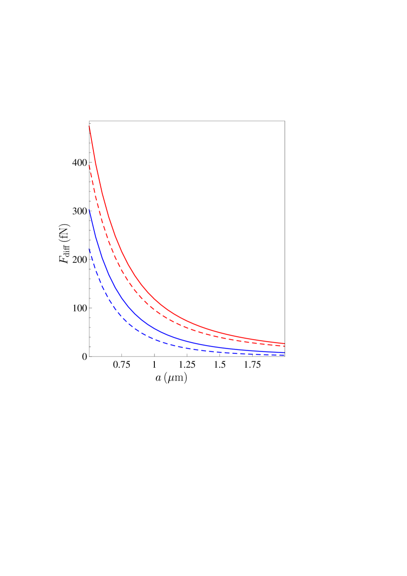
Computations have been performed at K taking for the thickness of the P-doped overlayer the value of nm and the value of nm for the thickness of the SiO2 layer. The computational results for the differential Casimir force are presented in Fig. 7 as functions of separation by the four lines corresponding to the four theoretical approaches (the top pair of solid and dashed lines is computed using the plasma model for Au with disregarded and taken into account free charge carriers in all dielectric materials, respectively, whereas the bottom pair of lines is obtained using the Drude model for Au and the same options for free charges in dielectrics).
As is seen in Fig. 7, all four theoretical approaches lead to widely distinct differential Casimir forces, which can be discriminated experimentally with certainty within the separation region from 0.5 to m. The computational results for the differential Casimir forces computed using the four theoretical approaches are presented in Table I over the separation region from 0.5 to m. The first column contains the value of separation. The second and third columns list the values of and computed using the plasma model for Au with disregarded and taken into account free charge carriers of dielectric materials, respectively. The fourth and fifth columns present the values of and obtained using the Drude model for Au with disregarded and taken into account free charge carriers of dielectric materials, respectively.
According to Table I, at m the differences between the predicted values and , between and , and between and are equal to 80.22, 92.06, and 80.17 fN, respectively. At and m the same differences are equal to 21.98, 38.86, and 21.98 fN and 8.49, 19.06, and 8.48 fN, respectively. All these values are far in excess of the experimental sensitivity.
If the plasma model for Au is used in computations, the relative deviation of the differential Casimir force obtained with disregarded free charge carriers in dielectrics from that found with taken free charge carriers into account is
| (43) |
From Table I one obtains that , 22.8%, and 24.7% at separations , 1.0, and m, respectively. The analogous deviation between the next two theoretical approaches defined as
| (44) |
is equal to 30.4%, 67.6%, and 124.4% at the same respective separations. Finally, the relative deviation of from is given by
| (45) |
At separation distances , 1.0, and m one obtains from Table I , 61.8%, and 124.0%, respectively. As to the relative deviation between the extreme two approaches, namely the one which disregards both the relaxation properties of electrons in metals and free charge carriers in dielectrics and the other which instead takes both into account, it is defined as
| (46) |
From Table I one obtains that , 233%, and 526.8% at the same respective separations. One can conclude that all the above relative deviations are sufficiently large for experimental discrimination between different theoretical approaches and all of them quickly increase with increasing separation.
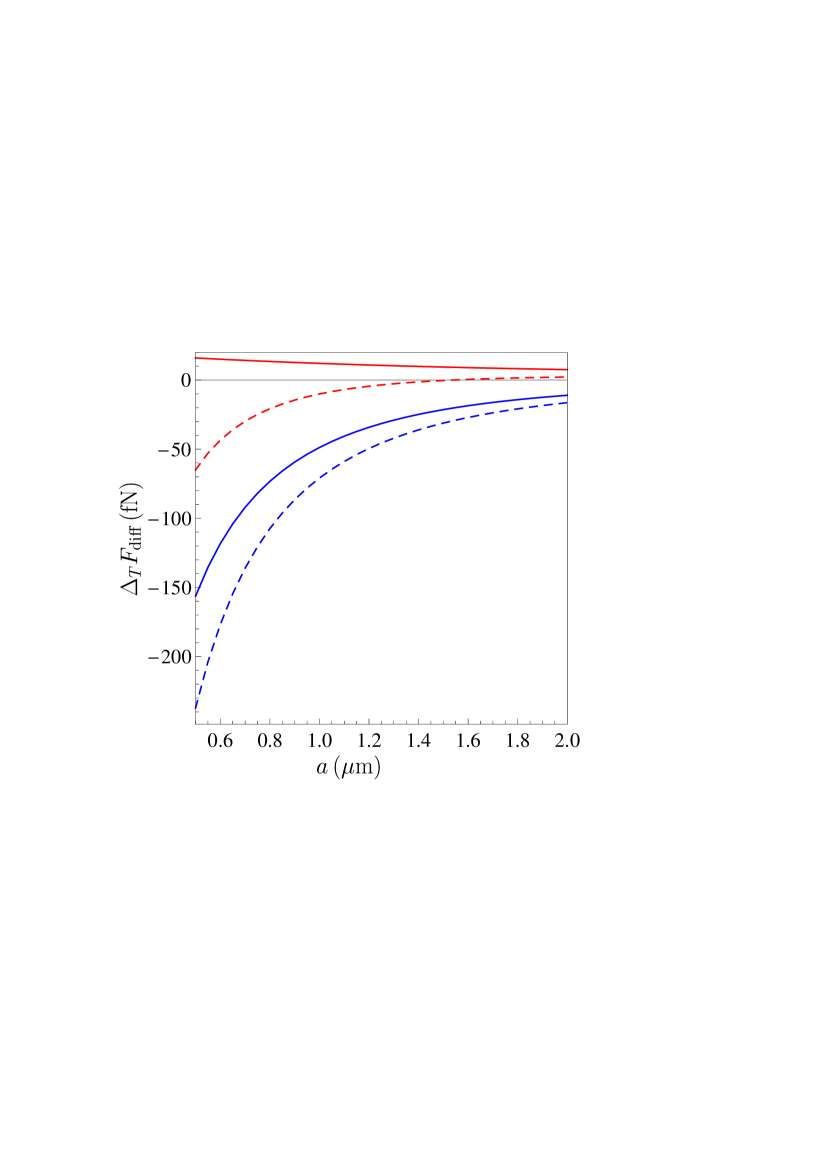
We have also computed the thermal correction (27) in the differential Casimir force in the configuration of Fig. 6 in the framework of the four theoretical approaches described above. The computational results at K are shown in Fig. 8 as functions of separation. The top pair of solid and dashed lines is obtained by using the plasma model for Au with disregarded and taken into account free charge carriers in dielectrics, respectively. The bottom pair of solid and dashed lines is computed by means of the Drude model for Au with respective neglect and inclusion of free charge carriers in dielectric materials. As can be seen in Fig. 8, over the separation range from 0.5 to m the thermal corrections predicted by the four theoretical approaches are significantly different and can be easily discriminated from each other taking into account the experimental sensitivity. Thus, at separations , 1.0, 1.5, and m the thermal correction using the plasma model with omitted conductivity of dielectrics, , is equal to 16.0, 12.1, 9.4, and 7.6 fN, respectively. In a similar way, for the remaining three theoretical approaches one has
| (47) | |||
at the same respective separations.
V Estimation of theoretical errors
Here, we present an estimation of errors inherent to the above computations. As was mentioned in Sec. III, a conservative estimation of the minimum detectable force in experiments of this type is fN. The total theoretical error in the determination of is contributed by several independent components and depends on separation.
We begin with a possible error in the concentration of free charge carriers in the P-doped overlayer (see Fig. 6). This error does not influence the computed values of and when the free charge carriers in dielectric materials are disregarded, but leads to the following errors if the free charge carriers are taken into account
| (48) |
where we present the values of errors at m and m. These results were obtained by repeating the computations of Sec. IV with .
The second error source in theoretical values of the differential Casimir force is uncertainty in the thickness of the SiO2 layer. For a commercial Si wafer nm leading to in our case. This leads to the following relative errors in our computational results:
| (49) | |||
The third source of theoretical errors is the error in the thickness of Si overlayer nm, i.e., resulting in
| (50) | |||
All these errors are random quantities characterized by a uniform distribution. In this case the total relative error is obtained by a summation of the respective errors (48)–(50) 2 ; 55
| (51) | |||
There is one more theoretical uncertainty originating from errors in the dielectric permittivities. At separations in the micrometer range, errors in the optical data do not lead to noticeable errors in the differential Casimir force. However, depending on the properties of a specific Au sample and its preparation process, the minimum possible value of the plasma frequency of Au was found to be eV 56 ; 57 . The corresponding value of the relaxation parameter is eV. In fact, different values of in the interval from 6.8 to 9.0 eV cannot be considered as random values of the measured quantity because they correspond to different samples. It would be preferable to determine the value of for the specific sample used in measurements of the Casimir force as it was done in Refs. 19 ; 20 . However, for illustrative purposes, here we present the relative deviations of the value of which would be obtained upon using for the plasma frequency the value instead of the value eV that was used above:
| (52) | |||
Some other effects which may influence the value of the differential force are the surface roughness and electrostatic patches. However, as it was noticed in Refs. 37 ; 37a ; 44a ; 44b ; 65 , the effect of patches is strongly suppressed in the differential force, whereas the effect of roughness is negligible in the micrometer separation range 2 ; 3 ; 37aa . Note that in comparison between the measurement data and theory in the proposed experiment one should correct the theoretical values in Table I for deviations from the proximity force approximation used in Eq. (3). This correction can be estimated as of about –0.2% of 21 ; 46 ; 47 ; 48 .
VI Conclusions and discussion
In the foregoing, we have suggested a universal setup allowing to directly measure the thermal effect in the Casimir force and to determine the role of free charge carriers in both metallic and dielectric materials, by a single experiment. According to our results, these aims can be achieved by measuring the differential Casimir force between a Au-coated sphere moving back and fourth above a structured plate covered with a conductive overlayer. One half of the plate is made of high-resistivity dielectric materials, while its other half is made of Au. The main novel feature of this setup is that the conductive overlayer is made of a doped semiconductor (P-doped Si in our case), whose concentration of free charge carriers is only slightly below the critical one, where the dielectric-to-metal phase transition occurs. Thus, the overlayer is made of a dielectric material possessing at room temperature a rather high conductivity, allowing for the electrostatic calibration required in precise measurements of the Casimir force.
We have considered two versions of the structured plate where the dielectric section is made either of bulk high-resistivity Si or of a layer of SiO2 followed by bulk high-resistivity Si. In both cases the differential Casimir force was calculated over the separation region from m to a few micrometers, i.e., in the domain where thermal effects determined by the zero-frequency term in the Lifshitz formula contribute considerably.
Computations have been performed within the four theoretical approaches discussed in the literature, i.e., Au at low frequencies is described by the plasma model and the free charge carriers in all dielectric materials (including the P-doped Si) are either disregarded or taken into account, or Au at low frequencies is described by the Drude model and the free charge carriers in all dielectric materials are again either disregarded or taken into account. We have also calculated the dependence of all differential forces on the thickness of the P-doped Si overlayer, determined the thermal contribution to the differential Casimir force at different separations and estimated all related errors and uncertainties.
The obtained results allow to conclude that all the four theoretical approaches lead to significantly different values of the differential Casimir force in the micrometer separation range, which are many times larger than both the experimental and theoretical errors. Thus, the proposed experiment is capable to provide an unequivocal confirmation to one of the above theoretical models and rule out the other three. Our calculation results show that the thermal effect in the differential Casimir force is up to two and one orders of magnitude larger than the minimum detectable signal when the Drude and plasma models are used, respectively. Because of this, the proposed experiment can not only lead to confirmation of one of the models, but it also allows reliable measurement of the thermal contribution to the observed signal.
One may guess which of the four above theoretical approaches has the best chances to be confirmed. As discussed in Sec. I, previous experiments with metallic test bodies 17 ; 18 ; 19 ; 20 ; 21 ; 22 ; 23 ; 38 are in agreement with the plasma model and exclude the Drude model, whereas only the experiment 25 leads to the opposite conclusion. Concurrently, several other experiments performed with dielectric test bodies 28 ; 29 ; 30 ; 31 ; 32 are in agreement with theory disregarding the free charge carriers and exclude theory taking the free charge carriers into account. On this basis, it is reasonable to expect that the proposed universal experiment may confirm the theoretical prediction obtained using the plasma model at low frequencies for Au with disregarded free charge carriers in dielectric materials. It should be underlined, however, that almost all of the abovementioned experiments (with exception of only Refs. 25 ; 28 ) are most precise at separations below m and use quite distinct experimental setups. This allows to conclude that the proposed universal experiment, which is capable to determine the role of free charge carriers in the Casimir force between any materials and measure the thermal effect in the micrometer separation range, will bring challenging results for the theory of electromagnetic fluctuations.
Acknowledgments
The work of V.M.M. was partially supported by the Russian Government Program of Competitive Growth of Kazan Federal University.
References
- (1) H. B. G. Casimir, Proc. Kon. Ned. Akad. Wet. B 51, 793 (1948).
- (2) M. Bordag, G. L. Klimchitskaya, U. Mohideen, and V. M. Mostepanenko, Advances in the Casimir Effect (Oxford University Press, Oxford, 2015).
- (3) G. L. Klimchitskaya, U. Mohideen, and V. M. Mostepanenko, Rev. Mod. Phys. 81, 1827 (2009).
- (4) A. W. Rodrigues, F. Capasso, and S. G. Johnson, Nature Photonics 5, 211 (2011).
- (5) L. M. Woods, D. A. R. Dalvit, A. Tkatchenko, P. Rodrigues-Lopez, A. W. Rodrigues, and R. Podgornik, Rev. Mod. Phys. 88, 045003 (2016).
- (6) V. A. Parsegian, Van der Waals Forces: A Handbook for Biologists, Chemists, Engineers, and Physicists (Cambridge University Press, Cambridge, 2005).
- (7) E. M. Lifshitz, Zh. Eksp. Teor. Fiz. 29, 94 (1955) [Sov. Phys. JETP 2, 73 (1956)].
- (8) M. Boström and Bo E. Sernelius, Phys. Rev. Lett. 84, 4757 (2000).
- (9) M. Bordag, B. Geyer, G. L. Klimchitskaya, and V. M. Mostepanenko, Phys. Rev. Lett. 85, 503 (2000).
- (10) V. B. Bezerra, G. L. Klimchitskaya, and V. M. Mostepanenko, Phys. Rev. A 65, 052113 (2002).
- (11) V. B. Bezerra, G. L. Klimchitskaya, and V. M. Mostepanenko, Phys. Rev. A 66, 062112 (2002).
- (12) V. B. Bezerra, G. L. Klimchitskaya, V. M. Mostepanenko, and C. Romero, Phys. Rev. A 69, 022119 (2004).
- (13) M. Bordag and I. G. Pirozhenko, Phys. Rev. D 82, 125016 (2010).
- (14) G. L. Klimchitskaya and C. C. Korikov, Phys. Rev. A 91, 032119 (2015); 92, 029902(E) (2015).
- (15) P. R. Buenzli and P. A. Martin, Phys. Rev. E 77, 011114 (2008).
- (16) G. Bimonte, Phys. Rev. A 79, 042107 (2009).
- (17) G. Bimonte, New J. Phys. 9, 281 (2007).
- (18) F. Intravaia and C. Henkel, Phys. Rev. Lett. 103, 130405 (2009).
- (19) F. Intravaia, S. A. Ellingsen, and C. Henkel, Phys. Rev. A 82, 032504 (2010).
- (20) R. S. Decca, E. Fischbach, G. L. Klimchitskaya, D. E. Krause, D. López, and V. M. Mostepanenko, Phys. Rev. D 68, 116003 (2003).
- (21) R. S. Decca, D. López, E. Fischbach, G. L. Klimchitskaya, D. E. Krause, and V. M. Mostepanenko, Ann. Phys. (N.Y.) 318, 37 (2005).
- (22) R. S. Decca, D. López, E. Fischbach, G. L. Klimchitskaya, D. E. Krause, and V. M. Mostepanenko, Phys. Rev. D 75, 077101 (2007).
- (23) R. S. Decca, D. López, E. Fischbach, G. L. Klimchitskaya, D. E. Krause, and V. M. Mostepanenko, Eur. Phys. J. C 51, 963 (2007).
- (24) C.-C. Chang, A. A. Banishev, R. Castillo-Garza, G. L. Klimchitskaya, V. M. Mostepanenko, and U. Mohideen, Phys. Rev. B 85, 165443 (2012).
- (25) A. A. Banishev, G. L. Klimchitskaya, V. M. Mostepanenko, and U. Mohideen, Phys. Rev. Lett. 110, 137401 (2013).
- (26) A. A. Banishev, G. L. Klimchitskaya, V. M. Mostepanenko, and U. Mohideen, Phys. Rev. B 88, 155410 (2013).
- (27) V. M. Mostepanenko, J. Phys.: Condens. Matter 27, 214013 (2015).
- (28) A. O. Sushkov, W. J. Kim, D. A. R. Dalvit, and S. K. Lamoreaux, Nature Phys. 7, 230 (2011).
- (29) V. B. Bezerra, G. L. Klimchitskaya, U. Mohideen, V. M. Mostepanenko, and C. Romero, Phys. Rev. B 83, 075417 (2011).
- (30) G. L. Klimchitskaya, M. Bordag, E. Fischbach, D. E. Krause, and V. M. Mostepanenko, Int. J. Mod. Phys. A 26, 3918 (2011).
- (31) J. M. Obrecht, R. J. Wild, M. Antezza, L. P. Pitaevskii, S. Stringari, and E. A. Cornell, Phys. Rev. Lett. 98, 063201 (2007).
- (32) F. Chen, G. L. Klimchitskaya, V. M. Mostepanenko, and U. Mohideen, Phys. Rev. B 76, 035338 (2007).
- (33) C.-C. Chang, A. A. Banishev, G. L. Klimchitskaya, V. M. Mostepanenko, and U. Mohideen, Phys. Rev. Lett. 107, 090403 (2011).
- (34) A. A. Banishev, C.-C. Chang, R. Castillo-Garza, G. L. Klimchitskaya, V. M. Mostepanenko, and U. Mohideen, Phys. Rev. B 85, 045436 (2012).
- (35) G. L. Klimchitskaya and V. M. Mostepanenko, J. Phys. A: Math. Theor. 41, 312002 (2008).
- (36) B. Geyer, G. L. Klimchitskaya, and V. M. Mostepanenko, Phys. Rev. D 72, 085009 (2005).
- (37) G. L. Klimchitskaya, U. Mohideen, and V. M. Mostepanenko, J. Phys. A: Math. Theor. 41, 432001 (2008).
- (38) B. Geyer, G. L. Klimchitskaya, and V. M. Mostepanenko, Ann. Phys. (N.Y.) 323, 291 (2008).
- (39) G. L. Klimchitskaya and C. C. Korikov, J. Phys.: Condens. Matter 27, 214007 (2015).
- (40) R. O. Behunin, D. A. R. Dalvit, R. S. Decca, C. Genet, I. W. Jung, A. Lambrecht, A. Liscio, D. López, S. Reynaud, G. Schnoering, G. Voisin, and Y. Zeng, Phys. Rev. A 90, 062115 (2014).
- (41) P. J. van Zwol, G. Palasantzas, and J. Th. M. De Hosson, Phys. Rev. B 77, 075412 (2008).
- (42) G. Bimonte, Phys. Rev. Lett. 112, 240401 (2014).
- (43) G. Bimonte, D. López, and R. S. Decca, Phys. Rev. B 93, 184434 (2016).
- (44) R. S. Decca, D. López, H. B. Chan, E. Fischbach, D. E. Krause, and C. R. Jamell, Phys. Rev. Lett. 94, 240401 (2005).
- (45) Y.-J. Chen, W. K. Tham, D. E. Krause, D. López, E. Fischbach, and R. S. Decca, Phys. Rev. Lett. 116, 221102 (2016).
- (46) G. L. Klimchitskaya and V. M. Mostepanenko, Phys. Rev. A 92, 042109 (2015).
- (47) G. L. Klimchitskaya and V. M. Mostepanenko, Phys. Rev. A 93, 042508 (2016).
- (48) G. L. Klimchitskaya and V. M. Mostepanenko, Phys. Rev. B 94, 045404 (2016).
- (49) G. L. Klimchitskaya and V. M. Mostepanenko, Phys. Rev. A 95, 012130 (2017).
- (50) G. Bimonte, Phys. Rev. Lett. 113, 240405 (2014).
- (51) G. Bimonte, Phys. Rev. B 91, 205443 (2015).
- (52) T. F. Rosenbaum, R. F. Milligan, M. A. Paalanen, G. A. Thomas, R. N. Bhatt, and W. Lin, Phys. Rev. B 27, 7509 (1983).
- (53) G. Bimonte, T. Emig, R. L. Jaffe, and M. Kardar, Europhys. Lett. 97, 50001 (2012).
- (54) G. Bimonte, T. Emig, and M. Kardar, Appl. Phys. Lett. 100, 074110 (2012).
- (55) L. P. Teo, Phys. Rev. D 88, 045019 (2013).
- (56) Handbook of Optical Constants of Solids, ed. E. D. Palik (Academic, New York, 1985).
- (57) Handbook of Optical Constants of Solids, vol. 2, ed. E. D. Palik (Academic, New York, 1991).
- (58) Quick Reference Manual for Silicon Integrated Circuit Technology, eds. W. E. Beadle, J. C. C. Tsai, and R. D. Plummer (Wiley, New York, 1985).
- (59) N. W. Ashcroft and N. D. Mermin, Solid State Physics (Saunders College, Philadelphia, 1976).
- (60) D. B. Hough and L. R. White, Adv. Coll. Interface Sci. 14, 3 (1980).
- (61) L. Bergström, Adv. Coll. Interface Sci. 70, 125 (1997).
- (62) S. G. Rabinovich, Measurement Errors and Uncertainties. Theory and Practice (Springer, New York, 2000).
- (63) V. B. Svetovoy, P. J. van Zwol, G. Palasantzas, and J. Th. M. De Hosson, Phys. Rev. B 77, 035439 (2008).
- (64) P. J. van Zwol, G. Palasantzas, M. van de Schootbrugge, and J. Th. M. De Hosson, Appl. Phys. Lett. 77, 054101 (2008).
- (65) R. O. Behunin, D. A. R. Dalvit, R. S. Decca, and C. C. Speake, Phys. Rev. D 89, 051301(R) (2014).
| (fN) | (fN) | (fN) | (fN) | |
|---|---|---|---|---|
| 0.5 | 474.57 | 394.35 | 302.29 | 222.12 |
| 0.6 | 336.31 | 278.28 | 202.96 | 144.96 |
| 0.7 | 248.13 | 204.43 | 141.86 | 98.18 |
| 0.8 | 189.07 | 155.13 | 102.39 | 68.46 |
| 0.9 | 147.94 | 120.90 | 75.88 | 48.86 |
| 1.0 | 118.36 | 96.38 | 57.52 | 35.54 |
| 1.2 | 80.00 | 64.72 | 34.94 | 19.67 |
| 1.4 | 57.27 | 46.10 | 22.56 | 11.40 |
| 1.6 | 42.87 | 34.38 | 15.32 | 6.84 |
| 1.8 | 33.26 | 26.61 | 10.86 | 4.21 |
| 2.0 | 26.56 | 21 22 | 7.98 | 2.64 |
| 2.2 | 21.72 | 17.34 | 6.07 | 1.68 |
| 2.4 | 18.11 | 14.46 | 4.74 | 1.09 |
| 2.6 | 15.36 | 12.26 | 3.80 | 0.71 |
| 2.8 | 13.20 | 10.55 | 3.12 | 0.46 |
| 3.0 | 11.48 | 9.19 | 2.61 | 0.31 |