Investigation of a possible electronic phase separation in the magnetic semiconductors Ga1-xMnxAs and Ga1-xMnxP by means of fluctuation spectroscopy
Abstract
We present systematic temperature-dependent resistance noise measurements on a series of ferromagnetic Ga1-xMnxAs epitaxial thin films covering a large parameter space in terms of the Mn content and other variations regarding sample fabrication. We infer that the electronic noise is dominated by switching processes related to impurities in the entire temperature range. While metallic compounds with % do not exhibit any significant change in the low-frequency resistance noise around the Curie temperature , we find indications for an electronic phase separation in films with % in the vicinity of , manifesting itself in a maximum in the noise power spectral density. These results are compared with noise measurements on an insulating Ga1-xMnxP reference sample, for which the evidence for an electronic phase separation is even stronger and a possible percolation of bound magnetic polarons is discussed. Another aspect addressed in this work is the effect of ion-irradiation induced disorder on the electronic properties of Ga1-xMnxAs films and, in particular, whether any electronic inhomogeneities can be observed in this case. Finally, we put our findings into the context of the ongoing debate on the electronic structure and the development of spontaneous magnetization in these materials.
pacs:
Valid PACS appear hereI Introduction
Diluted magnetic semiconductors (DMS) combine the benefits of semiconducting and magnetic materials and hence are most promising candidates for future spintronics applications Dietl and Ohno (2014); Dietl (2010). In particular, III-Mn-V DMS, as for instance the archetypal compound Ga1-xMnxAs, have been the subject of intensive research in the last two decades, motivated by both fundamental and technological interests Ohno (1998).
In Ga1-xMnxAs, as well as in the related compound Ga1-xMnxP, a few atomic percent of the nonmagnetic gallium host sublattice atoms are replaced with magnetic manganese atoms acting as acceptors. Both materials exhibit a long-range magnetic order of substitutional Mn ions mediated by holes Jungwirth et al. (2006, 2007); Scarpulla et al. (2005); Winkler et al. (2011). Crystalline defects—in particular Mn interstitials (MnI), which act as double donors and thereby compensate the hole doping, as well as As antisites (AsGa)—play a substantial role for both the strongly interrelated electronic and magnetic properties of DMS. Therefore, the preparation of high-quality samples is a delicate procedure and constitutes an obstacle to further enhancement of the Curie temperature beyond K for Ga1-xMnxAs Chen et al. (2009) and K for Ga1-xMnxP Farshchi et al. (2006).
Moreover, the effects of disorder Berciu and Bhatt (2001) and carrier-carrier interactions Richardella et al. (2010) make the theoretical description difficult Sato et al. (2010), and there is still no consensus on the development of spontaneous magnetization in these materials.
In literature, a broad spectrum of sometimes opposing theoretical approaches exists Samarth (2012), ranging from the assumption of free charge carriers König et al. (2003); Dietl et al. (2001, 2000); König et al. (2000) to the opposite case of strongly localized carriers Dobrowolska et al. (2012); Bhatt et al. (2002); Berciu and Bhatt (2001). While the first picture assumes the Fermi energy to lie within a merged band consisting of the valence band and a strongly broadened impurity band, the second model proposes the existence of a separate impurity band.
The latter, so-called impurity-band model is expected to be valid for weakly-doped samples. In this context, Kaminski and Das Sarma Kaminski and Sarma (2002, 2003) have developed an analytic polaron percolation theory for DMS ferromagnetism in the limit of strong charge carrier localization and for an inhomogeneous spatial distribution of magnetic impurities. In this model, the spins of localized charge carriers can polarize the surrounding magnetic impurities, leading to the emergence of bound magnetic polarons (BMP), which grow in size for decreasing temperatures and at low enough temperatures overlap until an infinite cluster is formed and spontaneous magnetization occurs Kumar et al. (2013).
Another conceivable scenario is that the p-d Zener model, which is equivalent to a weak-coupling RKKY picture and believed to be appropriate for more metallic systems with free charge carriers, can also be applied on the insulator side of the metal-insulator transition (MIT) of Ga1-xMnxAs. In this case, the hole localization length remains much greater than the average distance between the acceptors Ohno and Dietl (2008); Dietl (2006). Large mesoscopic fluctuations in the local value of the density of states near the MIT are expected to lead to a nano-scale phase separation into ferromagnetic and paramagnetic regions below , whereby the paramagnetic (hole-poor) regions can persist down to low temperatures, coexisting with ferromagnetic (hole-rich) bubbles.
Motivated by the still ongoing debate about the particular mechanisms of ferromagnetism and the crucial role of point defects, the present study focuses on a systematic investigation of low-frequency electronic transport properties on a series of Ga1-xMnxAs samples with different Mn contents and growth parameters. We apply fluctuation spectroscopy, a method which is sensitive to electric inhomogeneities on the nano- and micrometer scale and has been proven to be a versatile tool for identifying electronic phase separation and magnetically driven percolation, as observed, e.g., for perovskite manganites Podzorov et al. (2000) and more recently for the semimetallic ferromagnet EuB6 Das et al. (2012). Here, we aim to compare the noise behavior of metallic Ga1-xMnxAs films ( %) with rather insulating ( %) samples in order to gain further insight into possible percolative transitions and electronic phase separation. Moreover, we investigate another compound, Ga1-xMnxP, an even better candidate for the observation of a percolative transition. Despite its chemical similarity with Ga1-xMnxAs, Ga1-xMnxP has a Mn acceptor level lying four times deeper within the band gap, i.e. about eV above the valence band edge Clerjaud (1985). Therefore, it is obvious that the charge carriers are of a much more localized nature than in Ga1-xMnxAs. Nevertheless, hole-mediated ferromagnetism has also been demonstrated in Ga1-xMnxP Farshchi et al. (2006). In addition, Ga1-xMnxP is very similar to Ga1-xMnxAs concerning the magnetic anisotropy, spin-polarization and the scaling of as a function of the Mn concentration Zhou (2015). A comparison of weakly doped Ga1-xMnxAs with a Ga1-xMnxP sample ( %) may provide valuable information about possible commonalities and differences with regard to their noise characteristics and possible electronic inhomogeneities. Apart from varying the Mn content of the above mentioned compounds, an alternative approach for the control of magnetic and electronic properties is the irradiation with He ions, leading to the introduction of deep traps into the system and thereby to an increasing disorder. In this work, we therefore also address the question of which consequences ion irradiation has for the low-frequency resistance noise characteristics and whether signatures of an electronic phase separation or introduced defects can be observed for irradiated samples. It should be noted that fluctuation spectroscopy in general is highly suitable for studying the energy landscape of defects in semiconducting thin films Lonsky et al. (2016, 2015) and semiconductor heterostructures Müller et al. (2006a, b, 2015).
II Experimental Details
II.1 Sample Growth
Electronic transport measurements have been performed on a total of seven Ga1-xMnxAs thin film samples and one Ga1-xMnxP sample, see Table 1 for an overview. For all films, the corresponding Curie temperatures were determined by magnetization measurements Zhou et al. (2016); Hamida et al. (2014); Yuan et al. (2017); Zhou (2015). In general, a crucial parameter is the Mn content , but other factors as thermal annealing or induced disorder by ion irradiation also have a strong influence on the Curie temperature and the crystalline defect characteristics Hayashi et al. (2001); Potashnik et al. (2001); Esch et al. (1997); Sinnecker et al. (2010). The samples in this study were prepared in two different ways. Metallic Ga1-xMnxAs samples with % were grown by low-temperature molecular beam epitaxy (LT-MBE) on semi-insulating GaAs(001) substrates in a Mod Gen II MBE system with the lowest possible As2-partial pressure of about mbar at PTB in Braunschweig Hamida et al. (2014). After the growth of a nm high-temperature (HT) GaAs buffer layer at C, the temperature was decreased to C for the subsequent LT Ga1-xMnxAs growth. Post-growth annealing at C (18 hours in ambient atmosphere) was performed for one of the samples in order to enhance . The total Mn concentration was calculated from the molecular flux ratio of Mn and Ga measured in the MBE at the position of the wafer and compared with reflection high-energy electron diffraction (RHEED) and energy-dispersive X-ray spectroscopy (EDX) measurements. Moreover, three Ga1-xMnxAs samples with a nominal Mn concentration of % were grown by LT-MBE on semi-insulating GaAs(001) using a Veeco Mod III MBE system in Nottingham Zhou et al. (2016); Wang et al. (2008). In this case, thermal annealing was performed at C for 48 hours in ambient atmosphere and the Mn content was determined from the Mn/Ga flux ratio. Two of the films were irradiated with different doses of He ions after growth. This particular method allows to control the hole concentration and thus the electronic as well as the magnetic properties without changing the Mn content of a sample. The He-ion energy was chosen as keV. The fluences were cm-2 and cm-2 for the two irradiated samples. A better measure for the effect of irradiation on material properties than the fluence is the so-called displacement per atom (DPA), i.e. the number of times that an atom in the target is displaced during irradiation. This allows for a comparison with data reported in the literature, in which other ion species and energies are used. For the two irradiated samples, the DPA was and , respectively Zhou et al. (2016). During ion irradiation, the films were tilted by to avoid channeling. The irradiation parameters result in defects distributed roughly uniformly in the whole Ga1-xMnxAs layer as confirmed by simulations using the SRIM (Stopping and Range of Ions in Matter) code Ziegler et al. (1985). No measurable increase of Mn interstitials was observed by Rutherford backscattering spectroscopy (RBS) Zhou et al. (2016). Previous studies show that also the sheet concentration of substitutional Mn atoms remains constant Winkler et al. (2011), which is why we conclude that the main effect of He-ion irradiation is to introduce deep traps and thereby compensate the holes. It is well established that these defects reside in the As sublattice and most of them are primary defects related to vacancies and interstitials Sinnecker et al. (2010); Pons and Bourgoin (1985). In our case, atomic force microscopy (AFM) and RBS measurements do not show any indications of irradiation induced surface reconstruction. Further details can be found in Ref. Zhou et al. (2016). Finally, two Ga1-xMnxAs samples with low Mn contents of % and % as well as a Ga1-xMnxP sample with % were fabricated by ion implantation combined with pulsed laser melting in Dresden Yuan et al. (2017); Zhou (2015). Ion implantation is a common materials engineering technique for introducing foreign ions into a host material. In this case, Mn ions are implanted into GaAs or GaP wafers. The subsequent laser pulse drives a rapid liquid-phase epitaxial growth. The implantation energy was set to keV for GaAs Yuan et al. (2017) and keV for GaP Yuan et al. (2016); Zhou (2015). The wafer normal was tilted by with respect to the ion beam to avoid a channeling effect. A coherent XeCl laser (with nm wavelength and ns duration) was employed to recrystallize the samples, and the energy densities were optimized to achieve high crystalline quality and the highest Curie temperature. The optimal laser energy density is J/cm2 for Ga1-xMnxAs and J/cm2 for Ga1-xMnxP. The Mn concentration was determined by secondary ion mass spectroscopy. In contrast to films grown by LT-MBE, neither Mn interstitials nor As antisites are observed in samples prepared by ion implantation combined with pulsed laser melting Yuan et al. (2017); Cho et al. (2007). Transmission electron microscopy (TEM) studies prove the high crystalline quality of the films and exclude the presence of any extended lattice defects, amorphous inclusions and precipitates of other crystalline phases Yuan et al. (2017). For some selected films, an array of m2 Hall bars was defined by photolithography followed by wet chemical etching. The quality of Hall effect measurements thereby improves significantly due to a well-defined contact geometry and, as explained in more detail below, the resistance noise magnitude as the desired measurement signal increases due to smaller sample volumes according to Hooge’s law Hooge (1969, 1976). For all samples, electrical contacts were made by soldering In/Sn on top of the films. Charge carrier concentrations obtained from Hall effect measurements are given in Table 1. Due to the use of two different fabrication techniques and since the LT-MBE samples from Braunschweig and Nottingham were grown at different substrate temperatures and As-fluxes, care has to be taken in comparing the values for the hole concentration of films of different origin. Apart from that, as expected, the hole density increases after thermal annealing for the % samples and decreases with increasing ion irradiation dose for the % samples, cf. Section III.1 for more details. Furthermore, there is also a clear correlation between and . Finally, we point out that extensive studies on all present samples, including magnetization measurements and standard thin film characterization techniques, have been published elsewhere, cf. Ref. Hamida et al. (2014); Zhou et al. (2016); Yuan et al. (2017); Zhou (2015).
| Mn content | Fabrication | Source | Remarks | Thickness | ||
| Ga1-xMnxAs | ||||||
| 4.0 % | LT-MBE | PTB | as-grown, micro-structured | nm | K | |
| 4.0 % | LT-MBE | PTB | annealed (C, h), micro-structured | nm | K | |
| 6.0 % | LT-MBE | Nottingham | annealed (C, h) | nm | K | |
| 6.0 % | LT-MBE | Nottingham | annealed, He-ion irradiated (low dose) | nm | K | |
| 6.0 % | LT-MBE | Nottingham | annealed, He-ion irradiated (high dose) | nm | K | |
| 1.8 % | II+PLM | HZDR | as-grown, micro-structured | nm | K | |
| 1.2 % | II+PLM | HZDR | as-grown, micro-structured | nm | K | |
| Ga1-xMnxP | ||||||
| 3.5 % | II+PLM | HZDR | as-grown | nm | K |
II.2 Measurements
Electronic transport measurements have been performed using both AC and DC techniques. Experiments were carried out in a continuous-flow cryostat with variable temperature insert. Magnetic fields were applied perpendicular to the film plane. For some of the lithographically patterned Ga1-xMnxAs samples, low-frequency noise spectroscopy was conducted in a five-terminal AC setup, where the sample is placed in a bridge-circuit in order to suppress the constant DC voltage offset and to minimize external perturbations Scofield (1987). Other samples were measured in a four-terminal AC or DC setup. As a few samples showed a frequency-dependent resistivity at low temperatures, the excitation frequency was reduced from Hz down to Hz, or a DC noise measurement setup was utilized, which was verified to yield the same results as AC noise measurements. The fluctuating voltage signal is preamplified and processed by a spectrum analyzer yielding the voltage noise power spectral density (PSD) defined by:
| (1) |
where represents the fluctuating voltage drop across the sample and the angular frequency. Care was taken that all spurious sources of noise were minimized or eliminated. As required by Hooge’s empirical law Hooge (1969, 1976),
| (2) |
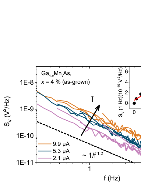
the magnitude of the voltage noise scales as , where represents the current flowing through the sample. Here, is the charge carrier density and the ’noisy’ sample volume, i.e. gives the total number of charge carriers in the material causing the observed noise. describes the frequency exponent which is commonly in the range for -type fluctuations. The Hooge parameter is widely used to compare the noise level of different systems and covers a range of – for different materials Raquet (2001). For bulk semiconductors, usually is of order –. Moreover, it is useful to normalize the magnitude of the voltage fluctuations with respect to the applied current, , and to the resistance of the sample, resulting in . Exemplary noise spectra for a Ga1-xMnxAs sample are presented in Fig. 1 for three different currents in a log-log plot. The dashed line represents a function with a slope of . The inset clarifies the quadratic scaling of with the current as predicted by Hooge’s law. Further details about the fluctuation spectroscopy technique can be found in Raquet (2001); Müller (2011).
III Results and Discussion
III.1 Ga1-xMnxAs films with high Mn content
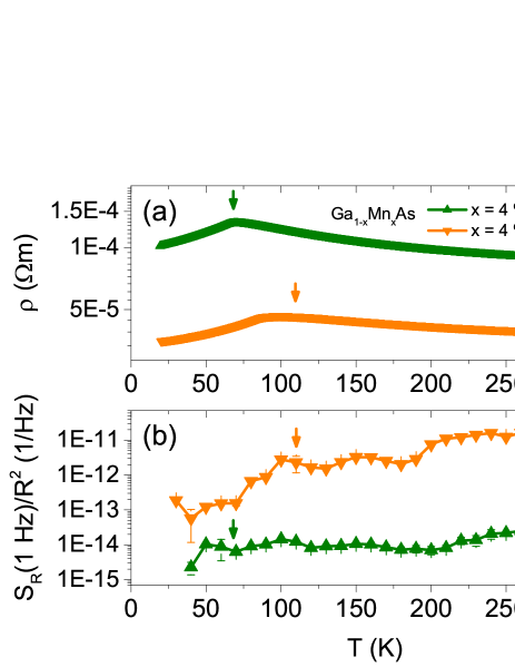
At first, we will discuss measurements on metallic films with Mn contents %. Resistivity curves of as-grown and annealed Ga1-xMnxAs samples with % are depicted in Fig. 2(a). As expected, typical maxima Matsukura et al. (1998) are observed in the vicinity of the samples’ respective Curie temperature . After post-growth annealing, the resistivity significantly decreases while increases compared to as-grown films. This effect can be explained by the out-diffusion of Mn interstitials to the film surface Edmonds et al. (2004). Commonly, these interstitials act as donors and compensate the hole-mediated ferromagnetism. Fig. 2(b) shows the corresponding normalized magnitude of the resistance fluctuations at Hz as a function of temperature in a semi-logarithmic representation. Remarkably, the PSD varies over several orders of magnitude for the two films and shows, in contrast to the resistivity, no significant features around . More specifically, there are no major changes in the noise behavior throughout the entire temperature range. In addition, a constant external out-of-plane magnetic field up to T does not lead to any changes in the normalized resistance noise (not shown, cf. Ref. Lonsky et al. (2017)). Possible contributions from mixed phases could be overshadowed by fluctuations related to thermally-activated impurity switching processes. However, more likely, due to the high concentration of Mn substitutional atoms, charge carriers are delocalized and the formation of magnetic polarons is not to be expected for these metallic samples. The observed -type noise is likely to be dominated by switching processes related to crystalline defects, which can also be seen in a strong variation of the Hooge parameter for the two different samples. At room temperature, we obtain for the as-grown and for the annealed film. Apparently, thermal annealing has a strong influence on the noise magnitude, leading to the presumption that slow fluctuation processes related to Mn interstitials might play an important role. Since thermal annealing reduces the density of Mn interstitials, one might expect a lower PSD for annealed samples, but the opposite is the case. The same behavior is observed for two % samples with a thickness of nm (not shown). Strikingly, for two further % films with a higher thickness of nm and similar values of , a slight decrease of the noise magnitude is observed after thermal annealing, indicating that the rearrangement of Mn interstitials due to diffusion processes towards the surface Edmonds et al. (2004), which become passivated due to oxidation or by binding with surplus As atoms, and concomitant surface effects may play an important role for the changes in the PSD after thermal annealing.
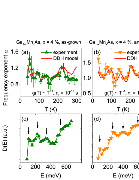
In order to deduce the characteristic energies of the switching processes contributing to the -type noise, we apply the phenomenological model of Dutta, Dimon and Horn (DDH) Dutta et al. (1979). In this model, a certain distribution of activation energies determines the temperature dependence of both the noise magnitude and the frequency exponent. An essential requirement for the applicability of this model is to check whether calculated after
| (3) |
agrees with the measured values. Here, represents an attempt time, usually between and s, corresponding to typical inverse phonon frequencies. Moreover, it is , where accounts for an explicit temperature dependence of the distribution of activation energies , which can be caused by a change of the number of thermally activated switching events (excitation of defect states) or of the coupling of fluctuations to the resistivity with temperature. As can be seen in Fig. 3(a) and (b), we find a good qualitative or even quantitative agreement between model and experiment for both % samples. This allows for calculating the distribution of activation energies,
| (4) |
of thermally activated fluctuators, which is shown in Fig. 3(c) and (d). Here, it is . Both samples show a similar behavior, namely an increase of towards higher activation energies, which we interpret as a superposition of several thermally activated processes with different energies, that can be attributed to various kinds of defects. In both cases, four local maxima in are observed and marked by black arrows in Fig. 3(c) and (d), whereby the values of the corresponding activation energies are remarkably similar for the two samples. It is plausible to assume that, due to the low growth temperatures utilized during LT-MBE, which are required in order to prevent phase separation within the material, a great variety of defects, such as Mn interstitials and As antisites, contribute to the distribution of activation energies. Although the energies of the local maxima are comparable to typical impurity binding energies in GaAs, care has to be taken when assigning the energies to specific defect states due to band gap renormalization in heavily doped semiconductors, which is accompanied by a shift of the respective binding energies.
Since no signatures of electronic phase separation can be identified for conventional metallic Ga1-xMnxAs samples with high Mn content ( %), we next focus on samples irradiated by He ions, whereby disorder in the films is enhanced by the introduction of deep traps, i.e. the Fermi level is shifted by means of carrier compensation in order to change the conductivity from metallic to insulating.
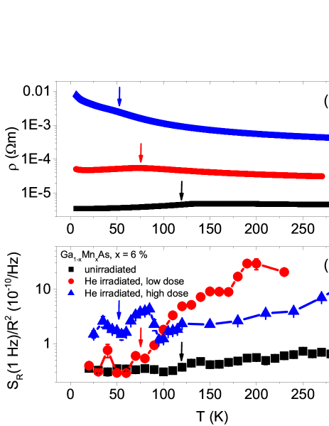
Fig. 4(a) shows resistivity data of three Ga1-xMnxAs samples with %. Point defects were introduced by the irradiation with an energetic He-ion beam using different doses as described in Section II.1 (fluences: cm-2 and cm-2, hereinafter referred to as ”low dose” and ”high dose”, respectively). The corresponding Curie temperatures determined from magnetization measurements are marked by arrows. While the unirradiated sample shows the lowest resistivity and metallic behavior with a relatively high of K, the resistivity increases strongly as a function of He-ion irradiation dose. At the same time, decreases down to K for the sample irradiated with a low He-ion dose and even further to K for a high irradiation dose. The typical maximum in resistivity Edmonds et al. (2002) becomes less pronounced for more insulating samples. These major changes in resistivity can be explained by an increase of the displacement per atom (DPA) for higher irradiation doses, which results in a decrease of the hole concentration. This is confirmed by Hall effect measurements at room temperature for the three samples (cf. Table 1).
The normalized temperature-dependent resistance noise PSD at Hz for the % samples is shown in Fig. 4(b) in a semi-logarithmic plot. The unirradiated sample has the lowest noise level over the entire temperature range. At temperatures below K, the PSD is nearly independent of temperature, followed by a slight increase above K towards room temperature. Likewise, below K, the film irradiated with a low He-ion dose shows the same constant noise magnitude, while there is a much stronger increase of nearly two orders of magnitude towards higher temperatures. The sample irradiated with the high dose shows the highest noise level of all three films below K, also followed by a characteristic increase for approaching room temperature. The great variation in the PSD for the different samples can be explained by the introduction of deep traps into the As sublattice. An exchange of charge carriers between such traps and the rest of the conducting material, resulting in fluctuations of the hole concentration, can cause the observed -type noise. As shown in previous studies Zhou et al. (2016), the concentration of Mn interstitials should not change as a function of irradiation dose, which implies that these interstitials are not the cause for the variation in the PSD as a function of He-ion irradiation dose, although they might still contribute to the noise. In addition, the noise data shown in Fig. 4(b) suggest a crossover between two temperature regimes: A temperature-independent region below about K and a characteristic increase of the noise magnitude, where the number of activated defects increases towards higher temperatures. The Hooge parameter at room temperature for these samples is of order – and therefore several orders of magnitude larger than for ’clean’ semiconductors. Furthermore, is also several orders of magnitude higher than for the % samples, presumably due to the higher Mn content, a higher concentration of traps in the case of the irradiated samples and different growth parameters (substrate temperature and annealing procedure).
Apart from that, no features around were observed except a slight increase below for the highest He-ion dose, which might be a hint for weak electronic phase separation or the increasing localization of charge carriers, and a pronounced peak at K. As shown in Ref. Lonsky et al. (2017), the application of the phenomenological model by Dutta, Dimon and Horn Dutta et al. (1979) allows to assign the enhanced noise magnitude at temperatures between 60 and 100 K to a distinct peak in the distribution of activation energies at energies of about meV. This energy can very likely be attributed to traps introduced by the strong He-ion irradiation. No changes in the normalized noise power were found in external magnetic fields up to T (cf. Ref. Lonsky et al. (2017)). Except the above-mentioned weak increase of the PSD below for the sample irradiated with the high dose, there are no indications for an electronic phase separation. As suggested by the large values of , possible contributions attributed to a percolative magnetic phase transition may be overshadowed by disorder effects or impurity switching processes. A different approach in order to find indications for a possible electronic phase separation is to tune the Mn content of Ga1-xMnxAs, which will be discussed in the following section.
III.2 Ga1-xMnxAs films with low Mn content and Ga1-xMnxP
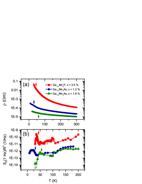
In this section, we focus on weakly doped Ga1-xMnxAs samples with localized charge carriers and compare the results with the metallic films and another insulating Ga1-xMnxP reference sample. Fig. 5(a) depicts the resistivity of two as-grown Ga1-xMnxAs samples with % and % and a Ga1-xMnxP film with %. In contrast to the metallic samples, no or only weak features around are visible in the resistivity. However, for all three films, the noise magnitude is significantly enhanced just below the respective Curie temperature, as can be seen in Fig. 5(b), where the normalized resistance noise at Hz is plotted versus temperature. For the % film, only a weak increase occurs around , followed by a sharp decrease towards lower temperatures. Although this compound is still to be considered as metallic, in the phase diagram it is located very close to the metal-insulator transition (MIT) Yuan et al. (2017), which is why weak signatures of an electronic phase separation are conceivable. The Ga1-xMnxAs film with % exhibits nearly the identical noise magnitude between and K, which is easily comprehensible since the same fabrication technique has been employed, the Mn content is very similar and hence the defect landscape contributing to the resistance noise is comparable. The calculated Hooge parameters at room temperature for both samples are also comparable, namely and for the % and the % films, respectively. However, the peak in the vicinity of is much more pronounced for the % sample, because this compound is situated right on the edge of the metal-insulator transition, cf. studies of electrical and magnetic properties on the present samples in Ref. Yuan et al. (2017). In detail, this sample still exhibits a global ferromagnetic behavior below , but electronic transport measurements indicate its insulating character. Within the framework of this study, no noise measurements on Ga1-xMnxAs samples situated on the insulating side of the MIT could be performed, because the maximum possible current was not sufficient to measure -type spectra reliably. Instead, the investigated Ga1-xMnxP sample is suggested to provide a reference example for the signatures of an electronic phase separation in fluctuation spectroscopy measurements of a diluted magnetic semiconductor with localized charge carriers. For this sample, the Hooge parameter at room temperature amounts to . As can be seen in Fig. 5(b), the Ga1-xMnxP film exhibits a pronounced peak just below , where the noise level increases by more than one order of magnitude in a small temperature interval. In analogy to previous studies on the semimetallic ferromagnet EuB6 Das et al. (2012), the diverging behavior of the resistance noise PSD for the Ga1-xMnxP sample can be described by a Lorentz function with a peak at K and a width K. In the case of EuB6, Das et al. attribute this sharp peak to a magnetic polaron percolation. As suggested by Kaminski and Das Sarma, such a behavior is also to be expected for Ga1-xMnxAs or Ga1-xMnxP samples with strongly localized charge carriers Kaminski and Sarma (2002, 2003). Due to the high defect concentration in DMS, it is assumed that the charge carrier concentration is highly inhomogeneous and as ferromagnetism is mediated by charge carriers, upon decreasing the temperature, the ferromagnetic transition will first occur locally within the regions with higher carrier concentration. Upon lowering the temperature, these finite-size clusters will grow and merge until the entire sample becomes ferromagnetic via a percolation transition.
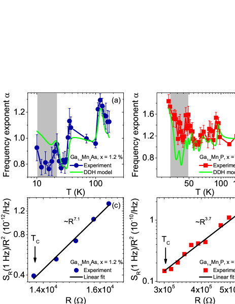
However, in contrast to semimetallic EuB6, where the ferromagnetic transition is accompanied by a drastic reduction of and a colossal magnetoresistance effect, the temperature dependence of the resistivity of the investigated insulating DMS samples is monotonic. For samples located in the vicinity of the metal-insulator transition, only a small kink is observable in around . In general, a ferromagnetic percolation transition is accompanied by an increase of the electrical conductivity, but, at the same time, this may be compensated by the increase of the resistivity with decreasing temperature due to the semiconducting nature of the material Kaminski and Sarma (2003). In the case of strongly localized charge carriers, the decrease in their hopping rate upon decreasing temperature overcomes the decrease in the hopping activation energy due to the ferromagnetic transition. Strikingly, although no features can be observed in the resistivity at , resistance noise, which is very sensitive to the microscopic current distribution in the sample, shows a strong peak for the Ga1-xMnxP sample. Due to the less localized nature of holes in the present weakly doped Ga1-xMnxAs samples, the possible percolation transition and thus the enhancement of the PSD are less pronounced. In addition, in the vicinity of the maximum in , we find a strong deviation between the calculated frequency exponents from Eq. (3) and the experimentally determined values, which is shown in Fig. 6(a) and (b) for the Ga1-xMnxAs ( %) and the Ga1-xMnxP samples, respectively. This non-applicability of the DDH model (marked by gray shaded areas) is another indication for a percolative transition Kogan (1996), since the assumptions of this phenomenological approach are not compatible with the nonlinear electronic transport behavior around the percolation threshold. The deviations between calculated and experimentally determined frequency exponents and the divergence in the PSD in the vicinity of the percolation threshold can be understood within the frame of a random resistor network (RRN) model Kogan (1996). The reduced number of effective current paths results in the suppression of cancellation of uncorrelated resistance fluctuations along different paths, which are abundant far away from Das et al. (2012). Around the current density is strongly inhomogeneous and the most significant contribution to the resistance noise comes from so-called bottlenecks which connect large parts of the infinite cluster. Here, the current density is higher than in other parts of the network. Rammal et al. have shown that near the percolation threshold , the PSD diverges as , while the resistance behaves as Rammal et al. (1985). Here, and are critical percolation exponents derived from a RRN model, and is the fraction of unbroken bonds of a RRN. Due to the non-accessibility of these exponents in an experiment, it is common to link the PSD and the resistance via with Yagil and Deutscher (1992). The corresponding analysis for the two relevant thin films is shown in Fig. 6(c) and (d), yielding a critical exponent for Ga1-xMnxP and for Ga1-xMnxAs ( %). While for Ga1-xMnxP this is in fair agreement with typical values for the exponent , e.g. for perovskite manganites Podzorov et al. (2000), the value for the Ga1-xMnxAs ( %) sample is exceptionally high. We note that no clear systematic changes of shape, position and height of the peak in the temperature-dependent PSD as a function of the applied out-of-plane magnetic field can be observed. It is assumed that possible changes as a function of the external field are too weak in order to be resolved.
We emphasize that the discussed picture of percolating bound magnetic polarons is expected to be only valid within the impurity-band model and is not compatible with the p-d Zener model, which assumes ferromagnetism being mediated by a Fermi sea of itinerant holes. The impurity-band model suggests that even for strong Mn doping the Fermi energy is located within the separate impurity band and only the degree of localization of the charge carriers will change. Our results support the view of holes being trapped in localized impurity band states for weakly doped Ga1-xMnxAs as well as for Ga1-xMnxP, whereas for metallic Ga1-xMnxAs samples with higher , where no signatures of a percolation mechanism were observed in the electronic noise, the widely-held view of delocalized holes within the valence band mediating ferromagnetism is more appropriate. We note that, for instance, DC transport and optical studies Jungwirth et al. (2007) as well as first-principle calculations Bae and Raebiger (2016) corroborate the applicability of the two different models on Ga1-xMnxAs for the respective Mn concentration ranges. Moreover, because of a strong variation of the Mn energy level among different III-Mn-V combinations, it is unlikely that all materials can be treated within a single model Khalid et al. (2014). As a consequence of the higher degree of hole localization in Ga1-xMnxP, the peak in is more pronounced as compared to the insulating Ga1-xMnxAs sample. An alternative interpretation of our findings for the Ga1-xMnxAs with small valid within the framework of the p-d Zener model could be an electronic phase separation in the vicinity of the metal-insulator transition Ohno and Dietl (2008); Dietl (2006), cf. Section I. In this case, the nano-scale phase separation results in the coexistence of ferromagnetic bubbles (metallic, hole-rich regime) and a paramagnetic matrix (insulating, hole-poor regime). However, this kind of electronic phase separation should persist in a broad temperature range below for insulating Ga1-xMnxAs samples with low Mn doping, which is not expected to result in such a pronounced and sharp peak in the temperature-dependent noise power spectral density as it was observed in this work. It should also be noted that all investigated samples show global ferromagnetism below , i.e. there are no mixed phases consisting of ferromagnetic clusters and superparamagnetic grains. Yuan et al. have shown that these mixed phases exist for Ga1-xMnxAs samples with %, but not for % Yuan et al. (2017). It is desirable to study the resistance noise behavior of such mixed phases in future.
IV Summary and Conclusion
In this work, we investigated the resistance noise on a series of Ga1-xMnxAs films with different manganese and defect concentrations and an insulating Ga1-xMnxP reference sample, all of which exhibit global ferromagnetism below . By applying the phenomenological model by Dutta, Dimon and Horn, we calculated the distribution of activation energies for several samples and discussed a superposition of different types of defects contributing to the measured -type noise. From the comparison of metallic and insulating samples we conclude that resistance noise in metallic Ga1-xMnxAs samples ( %) is mainly dominated by impurity switching processes and no prominent features occur around even in the presence of an external out-of-plane magnetic field, while insulating samples, in particular Ga1-xMnxP, show a sharp peak in the noise magnitude around which can be attributed to percolation processes in the material, for which we find a scaling behavior . Consequently, for Ga1-xMnxP, we infer that the picture of percolating magnetic polarons within the impurity-band model is applicable, while for Ga1-xMnxAs, this picture seems to be valid only for low Mn doping . These findings for samples with localized charge carriers are supported by clear deviations between the calculated (within the DDH model) and experimentally determined frequency exponents around the percolative transition. Besides varying the Mn content, another approach to tune Ga1-xMnxAs samples from the metallic side of the phase diagram towards the insulating regime is to irradiate the films with He ions. It was shown that fluctuation spectroscopy is sensitive to the changes in the defect landscape of irradiated samples, but no clear signs of electronic phase separation could be observed.
We have shown that a deeper understanding of defect physics and electronic phase separation in DMS can be obtained from fluctuation spectroscopy measurements. We suggest similar studies on other magnetic semiconductors which are supposed to exhibit percolation transitions or an electronic phase separation, like In1-xMnxAs or MnxGe1-x Park (2002).
Acknowledgements
The ion implantation was done at the Ion Beam Center (IBC) at HZDR. S. Z. acknowledges the financial support by the Helmholtz Association (VH-NG-713). We thank R. P. Campion from the University of Nottingham for supplying the Ga1-xMnxAs material for the He-ion irradiated samples.
References
- Dietl and Ohno (2014) T. Dietl and H. Ohno, Reviews of Modern Physics 86, 187 (2014).
- Dietl (2010) T. Dietl, Nature Materials 9, 965 (2010).
- Ohno (1998) H. Ohno, Science 281, 951 (1998).
- Jungwirth et al. (2006) T. Jungwirth, J. Sinova, J. Mašek, J. Kučera, and A. H. MacDonald, Reviews of Modern Physics 78, 809 (2006).
- Jungwirth et al. (2007) T. Jungwirth, J. Sinova, A. H. MacDonald, B. L. Gallagher, V. Novák, K. W. Edmonds, A. W. Rushforth, R. P. Campion, C. T. Foxon, L. Eaves, E. Olejník, J. Mašek, S.-R. E. Yang, J. Wunderlich, C. Gould, L. W. Molenkamp, T. Dietl, and H. Ohno, Phys. Rev. B 76, 125206 (2007).
- Scarpulla et al. (2005) M. A. Scarpulla, B. L. Cardozo, R. Farshchi, W. M. H. Oo, M. D. McCluskey, K. M. Yu, and O. D. Dubon, Phys. Rev. Lett. 95, 207204 (2005).
- Winkler et al. (2011) T. E. Winkler, P. R. Stone, T. Li, K. M. Yu, A. Bonanni, and O. D. Dubon, Appl. Phys. Lett. 98, 012103 (2011).
- Chen et al. (2009) L. Chen, S. Yan, P. F. Xu, J. Lu, W. Z. Wang, J. J. Deng, X. Qian, Y. Ji, and J. H. Zhao, Appl. Phys. Lett. 95, 182505 (2009).
- Farshchi et al. (2006) R. Farshchi, M. Scarpulla, P. Stone, K. Yu, I. Sharp, J. Beeman, H. Silvestri, L. Reichertz, E. Haller, and O. Dubon, Solid State Communications 140, 443 (2006).
- Berciu and Bhatt (2001) M. Berciu and R. N. Bhatt, Phys. Rev. Lett. 87, 107203 (2001).
- Richardella et al. (2010) A. Richardella, P. Roushan, S. Mack, B. Zhou, D. A. Huse, D. D. Awschalom, and A. Yazdani, Science 327, 665 (2010).
- Sato et al. (2010) K. Sato, L. Bergqvist, J. Kudrnovský, P. H. Dederichs, O. Eriksson, I. Turek, B. Sanyal, G. Bouzerar, H. Katayama-Yoshida, V. A. Dinh, T. Fukushima, H. Kizaki, and R. Zeller, Reviews of Modern Physics 82, 1633 (2010).
- Samarth (2012) N. Samarth, Nature Materials 11, 360 (2012).
- König et al. (2003) J. König, J. Schliemann, T. Jungwirth, and A. H. MacDonald, in Electronic Structure and Magnetism of Complex Materials (Springer Science Business Media, 2003) pp. 163–211.
- Dietl et al. (2001) T. Dietl, H. Ohno, and F. Matsukura, Phys. Rev. B 63, 195205 (2001).
- Dietl et al. (2000) T. Dietl, H. Ohno, F. Matsukura, J. Cibert, and D. Ferrand, Science 287, 1019 (2000).
- König et al. (2000) J. König, H.-H. Lin, and A. H. MacDonald, Phys. Rev. Lett. 84, 5628 (2000).
- Dobrowolska et al. (2012) M. Dobrowolska, K. Tivakornsasithorn, X. Liu, J. K. Furdyna, M. Berciu, K. M. Yu, and W. Walukiewicz, Nature Materials 11, 444 (2012).
- Bhatt et al. (2002) R. N. Bhatt, M. Berciu, M. P. Kennett, and X. Wan, Journal of Superconductivity: Incorporating Novel Magnetism 15, 71 (2002).
- Kaminski and Sarma (2002) A. Kaminski and S. D. Sarma, Phys. Rev. Lett. 88, 247202 (2002).
- Kaminski and Sarma (2003) A. Kaminski and S. D. Sarma, Phys. Rev. B 68, 235210 (2003).
- Kumar et al. (2013) S. Kumar, W. Paschoal, A. Johannes, D. Jacobsson, C. Borschel, A. Pertsova, C.-H. Wang, M.-K. Wu, C. M. Canali, C. Ronning, L. Samuelson, and H. Pettersson, Nano Letters 13, 5079 (2013).
- Ohno and Dietl (2008) H. Ohno and T. Dietl, Journal of Magnetism and Magnetic Materials 320, 1293 (2008).
- Dietl (2006) T. Dietl, Physica E: Low-dimensional Systems and Nanostructures 35, 293 (2006).
- Podzorov et al. (2000) V. Podzorov, M. Uehara, M. E. Gershenson, T. Y. Koo, and S.-W. Cheong, Phys. Rev. B 61, R3784 (2000).
- Das et al. (2012) P. Das, A. Amyan, J. Brandenburg, J. Mueller, P. Xiong, S. von Molnár, and Z. Fisk, Phys. Rev. B 86, 184425 (2012).
- Clerjaud (1985) B. Clerjaud, Journal of Physics C: Solid State Physics 18, 3615 (1985).
- Zhou (2015) S. Zhou, Journal of Physics D: Applied Physics 48, 263001 (2015).
- Lonsky et al. (2016) M. Lonsky, S. Heinz, M. V. Daniel, M. Albrecht, and J. Müller, J. Appl. Phys. 120, 142101 (2016).
- Lonsky et al. (2015) M. Lonsky, S. Heinz, M. Daniel, M. Albrecht, and J. Müller, in 2015 International Conference on Noise and Fluctuations (ICNF) (Institute of Electrical and Electronics Engineers (IEEE), 2015).
- Müller et al. (2006a) J. Müller, S. von Molnár, Y. Ohno, and H. Ohno, Phys. Rev. Lett. 96, 186601 (2006a).
- Müller et al. (2006b) J. Müller, Y. Li, S. von Molnár, Y. Ohno, and H. Ohno, Phys. Rev. B 74, 125310 (2006b).
- Müller et al. (2015) J. Müller, B. Körbitzer, A. Amyan, M. Pohlit, Y. Ohno, and H. Ohno, in 2015 International Conference on Noise and Fluctuations (ICNF) (IEEE, 2015).
- Zhou et al. (2016) S. Zhou, L. Li, Y. Yuan, A. W. Rushforth, L. Chen, Y. Wang, R. Böttger, R. Heller, J. Zhao, K. W. Edmonds, R. P. Campion, B. L. Gallagher, C. Timm, and M. Helm, Phys. Rev. B 94, 075205 (2016).
- Hamida et al. (2014) A. B. Hamida, S. Sievers, F. Bergmann, A. Racu, M. Bieler, K. Pierz, and H. W. Schumacher, Phys. Status Solidi B 251, 1652 (2014).
- Yuan et al. (2017) Y. Yuan, C. Xu, R. Hübner, R. Jakiela, R. Böttger, M. Helm, M. Sawicki, T. Dietl, and S. Zhou, Physical Review Materials 1, 054401 (2017).
- Hayashi et al. (2001) T. Hayashi, Y. Hashimoto, S. Katsumoto, and Y. Iye, Appl. Phys. Lett. 78, 1691 (2001).
- Potashnik et al. (2001) S. J. Potashnik, K. C. Ku, S. H. Chun, J. J. Berry, N. Samarth, and P. Schiffer, Appl. Phys. Lett. 79, 1495 (2001).
- Esch et al. (1997) A. V. Esch, L. V. Bockstal, J. D. Boeck, G. Verbanck, A. S. van Steenbergen, P. J. Wellmann, B. Grietens, R. Bogaerts, F. Herlach, and G. Borghs, Phys. Rev. B 56, 13103 (1997).
- Sinnecker et al. (2010) E. H. C. P. Sinnecker, G. M. Penello, T. G. Rappoport, M. M. Sant’Anna, D. E. R. Souza, M. P. Pires, J. K. Furdyna, and X. Liu, Phys. Rev. B 81, 245203 (2010).
- Wang et al. (2008) M. Wang, R. P. Campion, A. W. Rushforth, K. W. Edmonds, C. T. Foxon, and B. L. Gallagher, Applied Physics Letters 93, 132103 (2008).
- Ziegler et al. (1985) J. Ziegler, J. Biersack, and U. Littmark, The Stopping and Range of Ions in Solids (Pergamon Press, New York, 1985).
- Pons and Bourgoin (1985) D. Pons and J. C. Bourgoin, Journal of Physics C: Solid State Physics 18, 3839 (1985).
- Yuan et al. (2016) Y. Yuan, R. Hübner, F. Liu, M. Sawicki, O. Gordan, G. Salvan, D. R. T. Zahn, D. Banerjee, C. Baehtz, M. Helm, and S. Zhou, ACS Applied Materials & Interfaces 8, 3912 (2016).
- Cho et al. (2007) Y. J. Cho, M. A. Scarpulla, X. Liu, Y. Y. Zhou, O. D. Dubon, and J. K. Furdyna, in AIP Conference Proceedings (AIP, 2007).
- Hooge (1969) F. Hooge, Physics Letters A 29, 139 (1969).
- Hooge (1976) F. Hooge, Physica B 83, 14 (1976).
- Scofield (1987) J. H. Scofield, Rev. Sci. Instrum. 58, 985 (1987).
- Raquet (2001) B. Raquet, in Spin Electronics, Chapter: ”Electronic Noise in Magnetic Materials and Devices” (Springer, Heidelberg, 2001) pp. 232–273.
- Müller (2011) J. Müller, ChemPhysChem 12, 1222 (2011).
- Matsukura et al. (1998) F. Matsukura, H. Ohno, A. Shen, and Y. Sugawara, Phys. Rev. B 57, R2037 (1998).
- Edmonds et al. (2004) K. W. Edmonds, P. Bogusławski, K. Y. Wang, R. P. Campion, S. N. Novikov, N. R. S. Farley, B. L. Gallagher, C. T. Foxon, M. Sawicki, T. Dietl, M. B. Nardelli, and J. Bernholc, Phys. Rev. Lett. 92, 037201 (2004).
- Lonsky et al. (2017) M. Lonsky, J. Teschabai-Oglu, K. Pierz, S. Sievers, H. W. Schumacher, Y. Yuan, R. Böttger, S. Zhou, and J. Müller, Acta Physica Polonica A (accepted) (2017).
- Dutta et al. (1979) P. Dutta, P. Dimon, and P. M. Horn, Phys. Rev. Lett. 43, 646 (1979).
- Edmonds et al. (2002) K. W. Edmonds, K. Y. Wang, R. P. Campion, A. C. Neumann, C. T. Foxon, B. L. Gallagher, and P. C. Main, Appl. Phys. Lett. 81, 3010 (2002).
- Kogan (1996) S. Kogan, Electronic Noise and Fluctuations in Solids (Cambrigde University Press, 1996).
- Rammal et al. (1985) R. Rammal, C. Tannous, P. Breton, and A. M. S. Tremblay, Phys. Rev. Lett. 54, 1718 (1985).
- Yagil and Deutscher (1992) Y. Yagil and G. Deutscher, Phys. Rev. B 46, 16115 (1992).
- Bae and Raebiger (2016) S. Bae and H. Raebiger, Phys. Rev. B 94, 241115 (2016).
- Khalid et al. (2014) M. Khalid, E. Weschke, W. Skorupa, M. Helm, and S. Zhou, Phys. Rev. B 89, 121301 (2014).
- Park (2002) Y. D. Park, Science 295, 651 (2002).