Band nesting, massive Dirac Fermions and Valley Lande and Zeeman effects in transition metal dichalcogenides: a tight–binding model
Abstract
We present here the minimal tight–binding model for a single layer of transition metal dichalcogenides (TMDCs) MX2 (M–metal, X–chalcogen) which illuminates the physics and captures band nesting, massive Dirac Fermions and Valley Lande and Zeeman magnetic field effects. TMDCs share the hexagonal lattice with graphene but their electronic bands require much more complex atomic orbitals. Using symmetry arguments, a minimal basis consisting of 3 metal d–orbitals and 3 chalcogen dimer p–orbitals is constructed. The tunneling matrix elements between nearest neighbor metal and chalcogen orbitals are explicitly derived at , and points of the Brillouin zone. The nearest neighbor tunneling matrix elements connect specific metal and sulfur orbitals yielding an effective Hamiltonian giving correct composition of metal and chalcogen orbitals but not the direct gap at points. The direct gap at , correct masses and conduction band minima at points responsible for band nesting are obtained by inclusion of next neighbor Mo–Mo tunneling. The parameters of the next nearest neighbor model are successfully fitted to MX2 (M=Mo, X=S) density functional (DFT) ab–initio calculations of the highest valence and lowest conduction band dispersion along line in the Brillouin zone. The effective two–band massive Dirac Hamiltonian for MoS2, Lande g–factors and valley Zeeman splitting are obtained.
pacs:
I Introduction
There is currently renewed interest in understanding the electronic and optical properties of transition metal dichalcogenides (TMDCs) with formula MX2 (M - metal from group IV to VI, X=S, Se, Te) Connell et al. (1969); Bollinger et al. (2001); Mak et al. (2010); Splendiani et al. (2010); Radisavljevic et al. (2011); Kadantsev and Hawrylak (2012); Cheiwchanchamnangij and Lambrecht (2012); Xiao et al. (2012); Mak et al. (2012); Cao et al. (2012); Sallen et al. (2012); Kioseoglou et al. (2012); Wang et al. (2012); Jones et al. (2013); Ross et al. (2013); Mitioglu et al. (2013); Carvalho et al. (2013); Geim and Grigorieva (2013); Xu et al. (2014); Zhang et al. (2014a); Ye et al. (2014); Zhang et al. (2014b); Scrace et al. (2015); Withers et al. (2015); He et al. (2014); Wang et al. (2015a); Zhang et al. (2015); Arora et al. (2015); Jones et al. (2016). Recent experiments and ab–initio calculations show that while bulk TMDCs are indirect gap semiconductors, single layers are direct gap semiconductors with direct gaps at points of the Brillouin zone Connell et al. (1969); Bollinger et al. (2001); Mak et al. (2010); Splendiani et al. (2010); Radisavljevic et al. (2011); Kadantsev and Hawrylak (2012); Cheiwchanchamnangij and Lambrecht (2012); Xiao et al. (2012); Mak et al. (2012); Cao et al. (2012); Sallen et al. (2012); Kioseoglou et al. (2012); Wang et al. (2012); Jones et al. (2013); Ross et al. (2013); Mitioglu et al. (2013); Carvalho et al. (2013); Geim and Grigorieva (2013); Xu et al. (2014); Zhang et al. (2014a); Ye et al. (2014); Zhang et al. (2014b); Scrace et al. (2015); Withers et al. (2015); He et al. (2014); Wang et al. (2015a); Zhang et al. (2015); Arora et al. (2015); Jones et al. (2016). The existance of the gaps at points of the Brillouin zone (BZ) could be anticipated from graphene, as the two materials share the hexagonal lattice. If in graphene we were to replace one sublattice with metal atoms and second with chalcogen dimers, we might expect band structure similar to graphene but with opening of a gap at points in the BZ. If this analogy was correct, the gap opening in a spectrum of Dirac Fermions would lead to massive Dirac Fermions and nontrivial topological properties associated with broken inversion symmetry and valley degeneracy. However, in graphene the bandstructure can be understood in terms of a tight binding model with electrons tunneling between nearest neighbor’s orbitals. The results of ab–initio calculations Bollinger et al. (2001); Mak et al. (2010); Splendiani et al. (2010); Kadantsev and Hawrylak (2012); Cheiwchanchamnangij and Lambrecht (2012); Carvalho et al. (2013); Zhang et al. (2014a); Ye et al. (2014); Scrace et al. (2015) for MX2 show that the conduction band (CB) minima and valence band (VB) maxima wavefunctions are composed primarily of metal d–orbitals, i.e., next–nearest neighbors. If only metal orbitals are retained the lattice structure changes from hexagonal to triangular and the physics changes. Additional complication is the presence of secondary conduction band minima at points, at intermediate wavevectors between and points. These minima lead to conduction and valence band nesting which significantly enhances interactions of TMDCs with light Kadantsev and Hawrylak (2012); Carvalho et al. (2013). A tight–binding model which illuminates these aspects and allows for inclusion of magnetic field, confinement and many–body interactions is desirable.
There are already several tight-binding approaches to TMDCs by, e.g., Rostami et al. (2013), Liu et al. (2013), Cappelluti et al. (2013), Zahid et al. (2013), Fang et al. (2015) and others Ho et al. (2014); Liu et al. (2015); Ridolfi et al. (2015); Shanavas and Satpathy (2015); Silva-Guillen et al. (2016); Pearce et al. (2016); Wu et al. (2015) as well as approaches by Kormányos et al. (2015). Each contribution brings new physics and adds on to our understanding of TMDCs. In this work we build on previous theoretical works as well as our ab–initio results Kadantsev and Hawrylak (2012); Scrace et al. (2015) to develop the simplest tight–binding model which illuminates the physics of TMDCs, especially the role of hexagonal lattice, tunneling from metal to dimer orbitals, band nesting, effective two band massive Dirac Fermion model, Lande g–factors and valley Zeeman splitting and Landau levels.
II The model
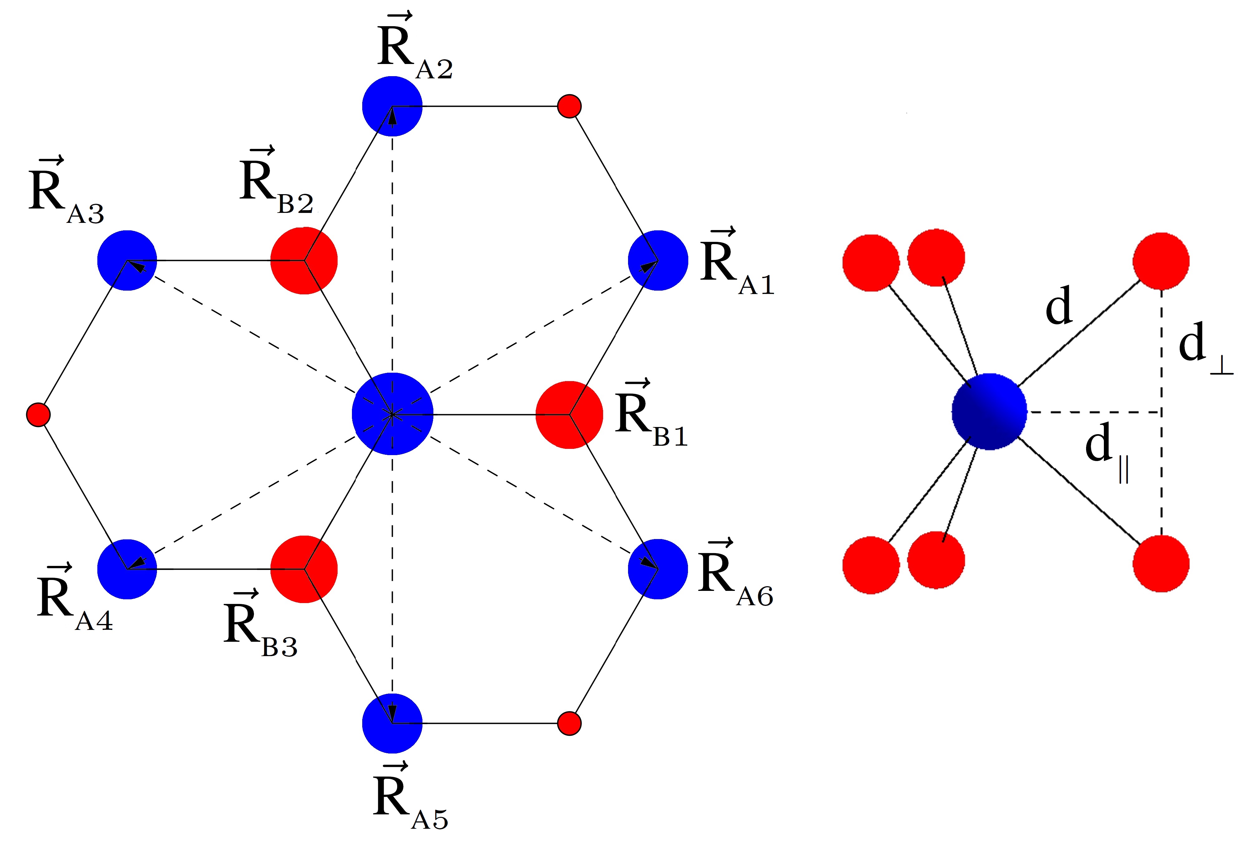
We start with the structure of a single layer of MX2 and for definiteness we focus on MoS2. Fig. 1 shows the top view of a fragment of MoS2 hexagonal lattice, with Mo positions marked with blue circles and sulfur dimers marked with red circles. The lattice structure is almost identical to graphene, the differences are visible in the side view showing the sulfur dimers and three, sulfur - metal - sulfur, layers of a single layer of MoS2. Fig. 1 shows a central metal atom (large blue circle) of sublattice A surrounded by three first neighbor sulfur dimers of sublattice B marked with positions , and . The positions of second neighbors belonging to metal sublattice A are marked with ,…,. We now construct the wavefunction out of orbitals localized on metal atoms and sulfur dimers. We start by selecting orbitals on a metal atom. Guided by results of ab–initio calculations Kadantsev and Hawrylak (2012) we first consider d–orbitals ,with . Out of 5 orbitals, orbitals with are even with respect to the Mo layer. We select three d–orbitals localized on i-th Mo atom of sublattice A at . For a sulfur dimer we select 3 p orbitals with on lower (L) and upper (U) sulfur atoms. We first construct dimer orbitals which are even with respect to the Mo plane:
and
We note the minus sign in the orbital due to odd character of orbital. With 3 orbitals on Mo atom we can write the wavefunctions on the sublattice A for each wavevector and orbital as:
| (1) |
where is number of unit cells. In the same way we can write the three wavefunctions for sublattice B of sulfur dimers:
| (2) |
We now seek the LCAO electron wavefunction with coefficients , for band and wavevector to be obtained by diagonalizing the Hamiltonian matrix in the space of wavefunctions and .
III The nearest-neighbor tunneling Hamiltonian
We now proceed to construct matrix elements of the Hamiltonian describing tunneling from Mo orbitals to sulfur dimer orbitals. The matrix elements for tunneling from Mo atom in Fig. 1 to it’s 3 nearest–neighbors , and can be explicitly written in analogy to graphene:
| (3) |
where is a potential on sublattice A. We can evaluate matrix elements, Eq. 3, at the point of the Brillouin zone to obtain
| (4) |
where is a Slater–Koster matrix element for tunneling from Mo atom orbital to nearest sulfur dimer orbital . We see in Eq. 4 that tunneling from central Mo atom to three nearest neighbor sulfur dimers generates additional phase factors which depend on the angular momentum of orbitals involved. The pairs of orbitals giving non–vanishing tunneling matrix element must satisfy selection rule . The only pairs of orbitals which satisfy this rule at point are:
| (5) |
Hence the Hamiltonian at the point is block–diagonal. Similar calculations lead to different selection rules at the nonequivalent point:
| (6) |
while at the point different pairs of orbital are coupled:
| (7) |
We see that the three orbitals are coupled to a different dimer orbital each. Which pairs are coupled depends on the and points. This has important consequences for the response to magnetic field discussed later. We can now write tunneling Hamiltonian with first– nearest–neighbor tunneling only. Here we put together the group of 3 degenerate d orbitals of Mo and a group of three degenerate p-orbitals of S2. The tunneling matrix elements depend on tunneling amplitudes with dependence on expressed by functions . The function is the only function finite at . Looking at the tunneling matrix elements of Hamiltonian, Eq. 14, containing gives the coupled pairs of orbitals given by Eq. 5. Explicit forms of and are given in the Appendix A.
| (14) |
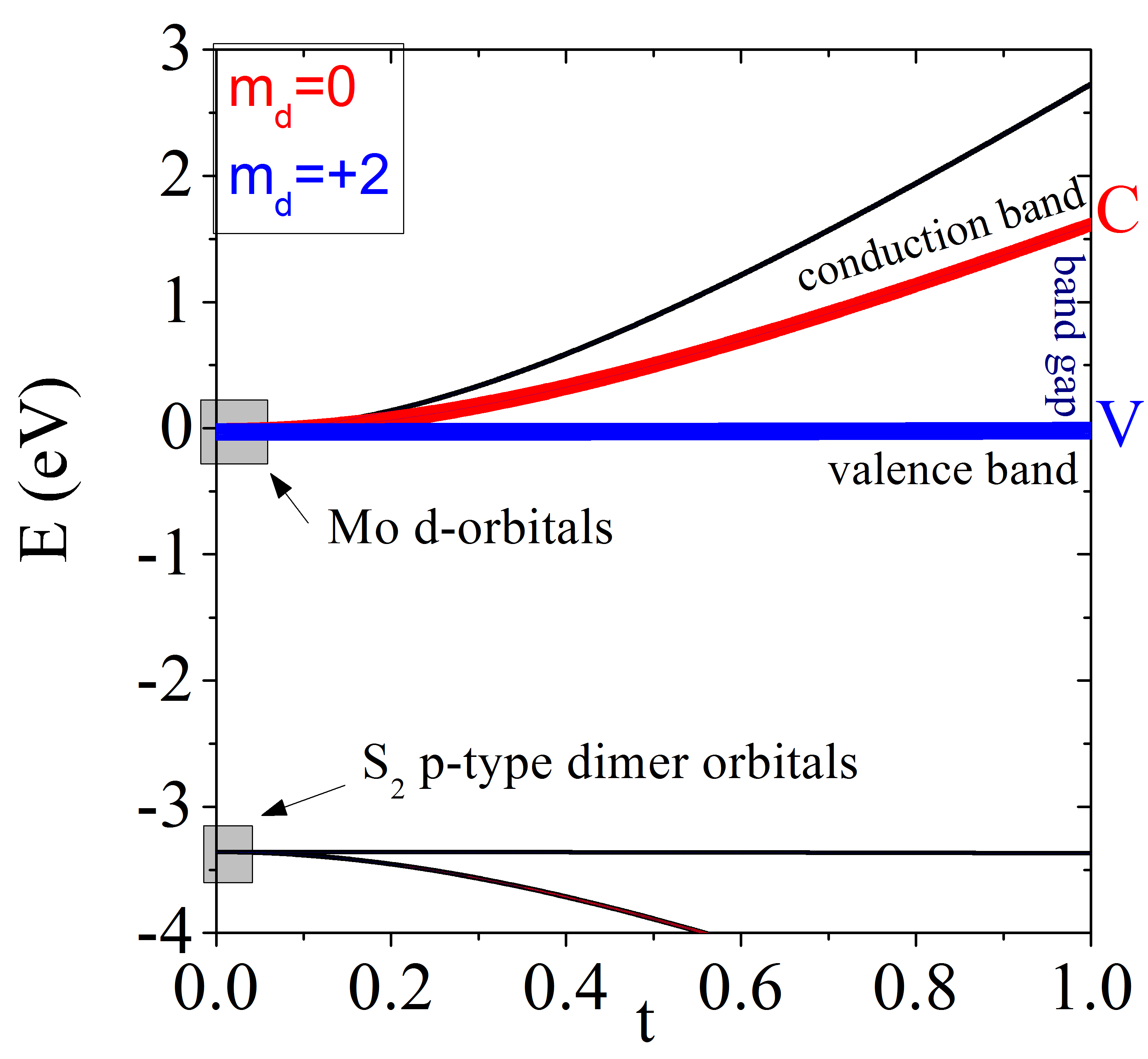
We parameterize tunneling matrix elements, , of Eq. 14 with tunneling parameter . means no tunneling and means full tunneling matrix, Eq. 14. Fig. 2 shows the evolution of the energy spectrum of the first–nearest–neighbor Hamiltonian at K point, Eq. 14, as a function of tunneling strength . At we have 3 degenerate -orbitals with energies and 3 degenerate -orbitals on sulfur dimers with energy . As the tunneling from Mo to S2 orbitals is turned on the degeneracy of -orbitals is removed as they start hybridizing with -orbitals. The orbital is the lowest energy valence band orbital. The evolves as a conduction band orbital and gives rise to the higher energy conduction band orbital. The magnitude of the bandgap is fitted to the ab–initio result using ABINIT and ADF Kadantsev and Hawrylak (2012); Scrace et al. (2015).
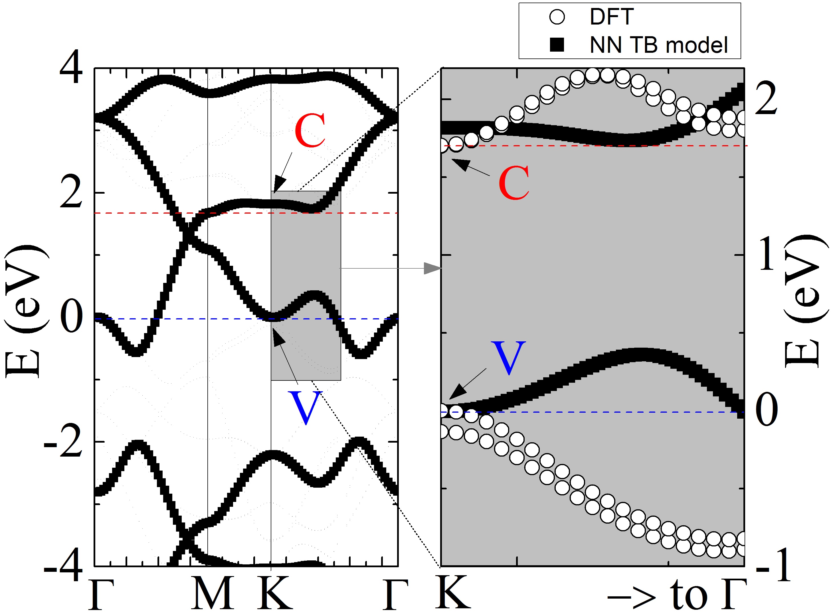
Fig. 3 shows the energy bands across the BZ obtained by fitting the first neighbor Hamiltonian, Eq. 14, using genetic algorithm to ab–initio results obtained using ABINIT Kadantsev and Hawrylak (2012); Scrace et al. (2015). We see that such a simple Hamiltonian predicts a correct, finite, gap at point but it also predicts closing of the gap in the Brillouin zone, here shown between and points. The closing of the gap is a consequence of the reversal of the role of d–orbital: it is a conduction band orbital at point but valence band orbital at . Therefore without level repulsion there must be closing of the gap. In the right panel we also show close up of the dispersion of valence and conduction band along the line. We see that the gap at point is correct but the masses of holes and electrons are incorrect, leading to the lowest energy gap away from the point and a lack of CB maximum at the point. Hence the simplest nearest-neighbor tunneling model which successfully describes Dirac Fermions in graphene captures the opening of the gap at point of the BZ and composition of VB and CB wavefunctions in terms of –Mo and –S2 orbitals. However, it fails to capture important properties of CB and VB away from the points. In order to capture the effective masses of CB and VB bands and CB maximum leading to band nesting we need to include tunneling between second neighbor Mo atoms.
IV The first and second neighbor tunneling Hamiltonian
We now consider tunneling from Mo atom to its 6 nearest neighbors Mo atoms as illustrated in Fig. 1, with same for sulfur dimers. The second neighbor tunneling matrix elements are parameterized by tunneling amplitudes with dependence on expressed by functions . Explicit forms of and are given in the Appendix B. The explicit form of the Hamiltonian contains now dispersion of and coupling between and orbitals:
| (21) |
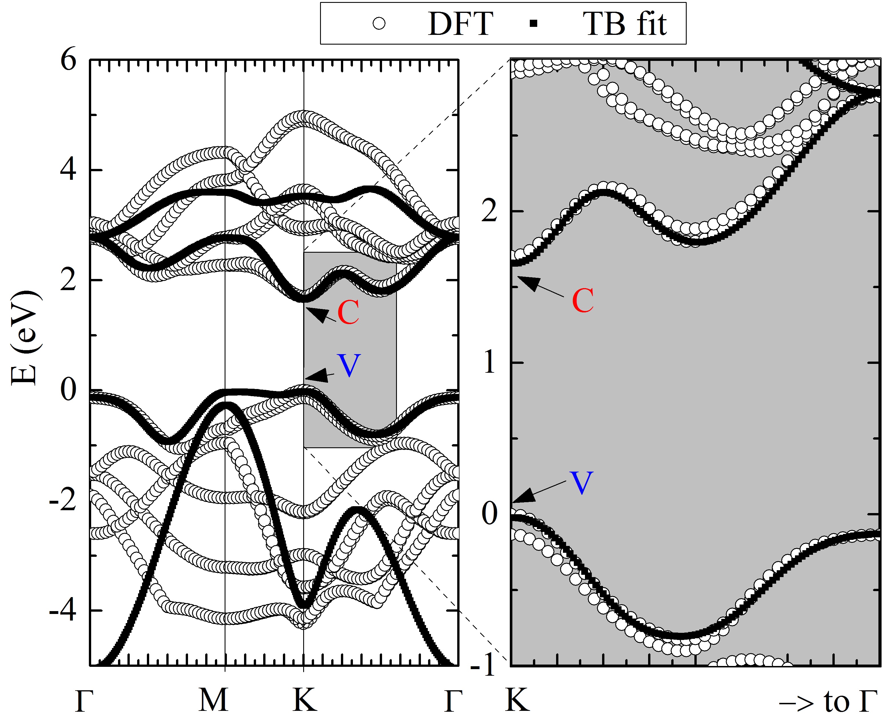
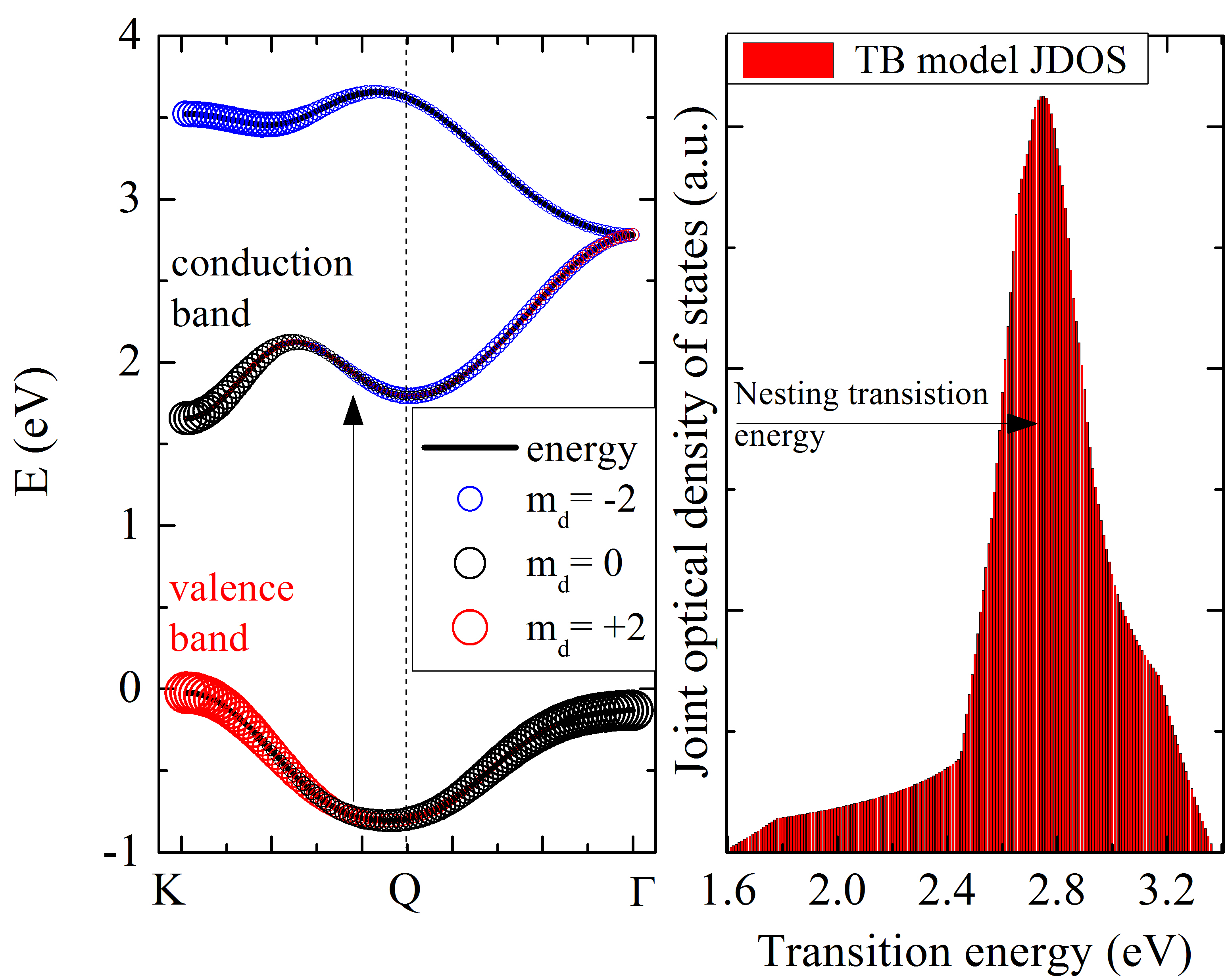
Fig. 4 shows the energy bands obtained using first and second neighbor Hamiltonian, Eq. 21, black squares, and ab–initio energy bands without spin–orbit (SO) coupling. We see that the gap opens up across the entire BZ due to direct interaction of –orbitals. The right hand side of the figure shows excellent agreement of ab–initio and TB, Eq. 21, conduction (CB) and valence (VB) energy bands. In particular, we see the second minimum in the CB at point. The origin of the minimum at point is analyzed in the left panel of Fig. 5 where different colors mark contributions from different -orbitals. The size of circles denotes the contribution of different orbitals. At the point the top of the VB is composed mainly of orbital and bottom of CB has character. At point top of the VB has character and bottom of the CB has character. Hence the higher energy band with character has to cross the CB. The crossing of and bands leads to a maximum in the conduction band followed by a second minimum at . Around the minimum at point the conduction and valence bands are parallel. The nesting of CB and VB leads to a maximum in joint optical density of states, shown in the right panel of Fig. 5 and discussed already by, e.g., Castro–Neto and co–workers Carvalho et al. (2013).
V Effective two-band massive Dirac fermion model
With the 6-band model understood we now proceed to fit our results to the two–band massive Dirac Fermion model applicable in the vicinity of points. Following Kormányos et al. (2015) we write our two–band Hamiltonian as a function of deviation from the wavector as:
| (22) |
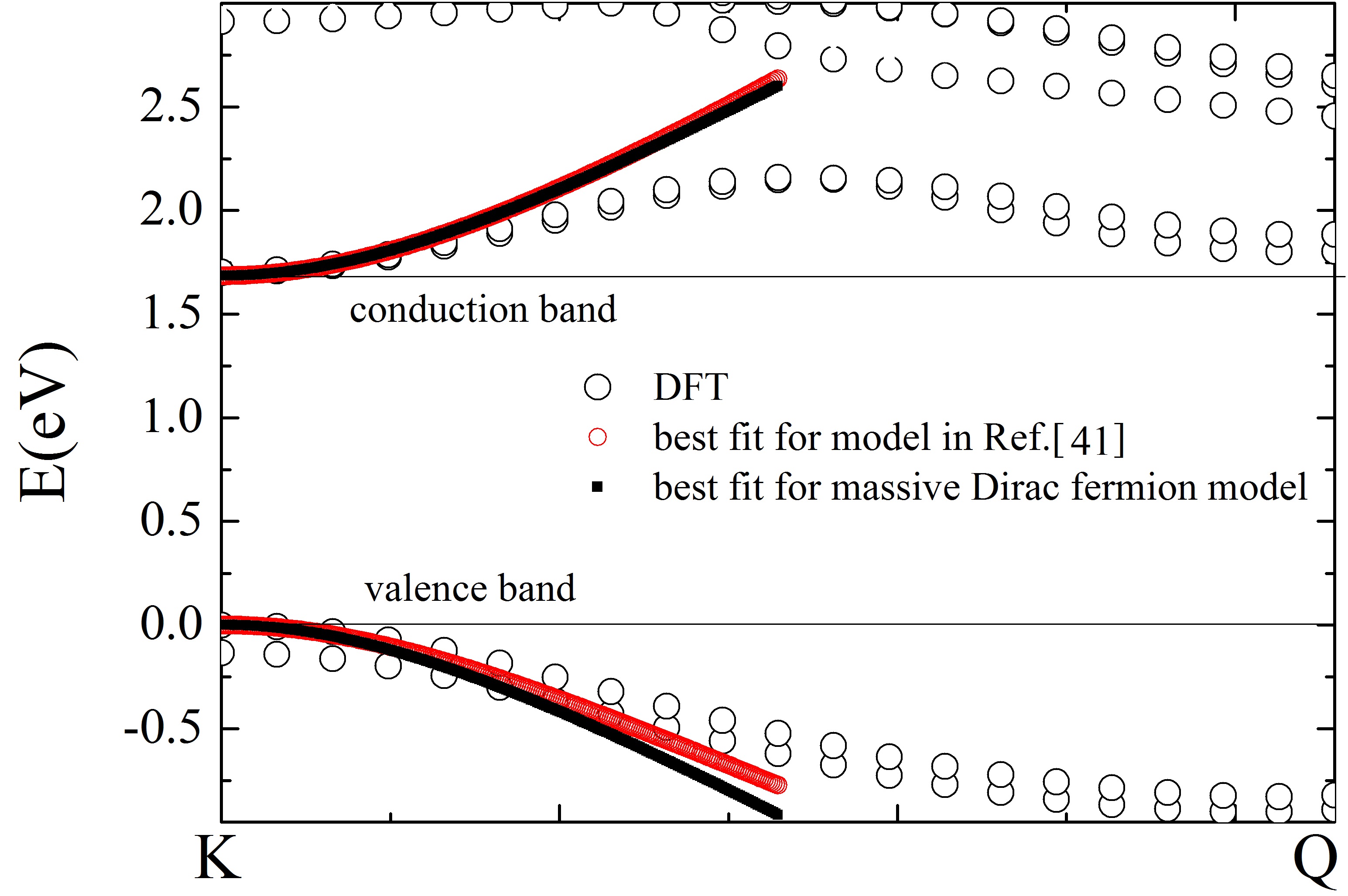
where and for , valley’s. Fig. 6 shows the results of fitting eigenenergies of Eq. 22 to our ab–initio results and results obtained by theory of Kormányos et al. (2015). We see a good agreement of all three results. The two–band model parameters used in Fig. 6 are Å, eV, eV, eVÅ2, eVÅ2, eVÅ2, eVÅ3. For Eq. 22 reduces to a massive Dirac Fermion model proposed by Xiao et al.[8] for the description of conduction and valence bands close to the point. Note that wavevector is measured from the point. Best parameters for massive Dirac Fermion model are Å, eV and eV.
VI Magnetic field - Lande g-factors
We now describe response of TMDC’s to the applied magnetic field Sallen et al. (2012); Scrace et al. (2015); Ho et al. (2014); Shanavas and Satpathy (2015); Goerbig et al. (2006); Xiao et al. (2007); Stier et al. (2016); Wang et al. (2015b); MacNeill et al. (2015); Li et al. (2014); Aivazian et al. (2015); Srivastava et al. (2015); Zeng et al. (2012); Plechinger et al. (2016); Mitioglu et al. (2016); Wang et al. (2016a, b); Cai et al. (2013). The perpendicular magnetic field couples to the orbital angular momentum as . From symmetry analysis at the point the wavefunctions of conduction band are composed of and orbitals as:
| (23) |
With details of the analysis found in the Appendix C the energy of electron in CB at point is given by the contributions from the orbital, equal to zero, and finite contribution from orbital as
At point the energy of electron in CB is given by the contributions from the orbital (no contribution) and contribution from orbital as
The valley Lande energy splitting in the conduction band is given by
| (24) |
where we used the fact that orbital compositions of orbitals at and are equal. A similar analysis carried out for the valley Lande energy splitting in the valence band gives . Using results from the 6 band model, Eq. 21, gives the effective Lande g–factors of in the conduction band and . By comparison, values deduced from Ref.[Fang et al., 2015] give and those from Ref.[Cappelluti et al., 2013] give .
VII Magnetic field - valley Zeeman and Landau g-factors
We now discuss valley Zeeman splitting due to Landau quantization. We start with the massive Dirac Hamiltonian for point derived in Eq. 22:
| (25) |
With magnetic field in the symmetric gauge, vector potential . We substitute , measure length in units of magnetic length , where . Transformation into creation and annihilation operators Hawrylak (1993)
| (26) |
gives massive Dirac Fermion Hamiltonian in magnetic field as
| (27) |
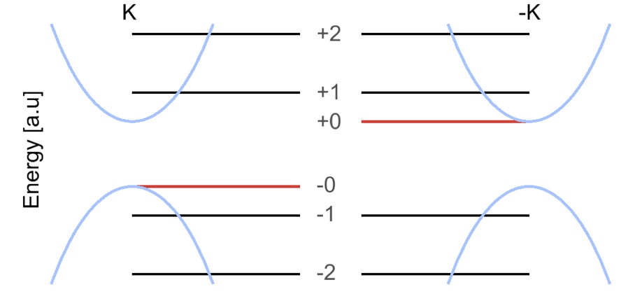
where . The eigenfunctions of Hamiltonian, Eq. 27, are spinors in the basis of CB and VB states at (), with eigenenergies of the n Landau level . Here, massive Dirac Fermion nature manifests itself in eigenvectors expressed as a combination of states with different , which differs for both valleys. The energy spectrum contains three types of states for and points: positive (negative) energies with for conduction (valence) band states indicated by indices C(V) and Landau level (0LL) in each valley. The key result Goerbig et al. (2006); Xiao et al. (2007) is that in the valley the 0LL is attached to the top of the valence band (negative energy) while in the valley 0LL is attached to the bottom of the conduction band (positive energy). Fig. 7 shows the energy spectrum for and valleys, with LL shown in red.
The valley Zeeman splitting in the conduction band is given by the energy difference between electron in valley, and electron in the valley :
| (28) |
where is the cyclotron energy. We see that valley Zeeman splitting is proportional to the cyclotron energy and the ratio of Fermi velocity to the energy gap Cai et al. (2013).
We can now compare the valley Lande and Zeeman contributions for MoS2. For magnetic field T, we obtain the following values of splitting:
| (29) |
| (30) |
| (31) |
First two values are in excellent agreement with recently reported Stier et al. (2016) experimental Lande splitting of approximately meV .
We now discuss the effect of spin-orbit interaction on the Landau level spectrum. The Hamiltonian for both spin down and up at the point can be written as:
| (36) |
where is the spin splitting for conduction (valence) band. In analogy with Eq. 27 we obtain the eigenvectors for and eigenvectors for the valley. The corresponding eigenvalues are given by , where for spin up or down. The LL spectrum becomes even more asymmetric between the valleys. Because of the interaction between valence and conduction band the strong SO coupling in the valence band leads to spin splitting in the conduction band.
VIII Conclusions
We presented here a tight–binding theory of transition metal dichalcogenides. We derived an effective tight binding Hamiltonian and elucidated the electron tunneling from metal to dichalcogenides orbitals at different points of the BZ. This allowed us to discuss the band gaps at points in the BZ, the origin of secondary conduction band minima at points and their role in band nesting and strong light matter interaction. The Lande and Zeeman valley splitting as well as the effective mass Dirac Fermion Hamiltonian in the magnetic field was determined.
Acknowledgements.
MB acknowledges financial support from National Science Center (NCN), Poland, grant Sonata No. 2013/11/D/ST3/02703. L.SZ and P.H. acknowledge support from NSERC and uOttawa University Research Chair in Quantum Theory of Materials, Nanostructures and Devices. One of us (PH) thanks J. Kono, S. Crooker, A. Stier and M. Potemski for discussions.Appendix A Nearest neighbor matrix elements
Matrix elements of nearest neighbor tunneling Hamiltonian, Eq. 14, are expressed by -independent parameters
| (37) |
and -dependent factors
| (38) |
Appendix B Next nearest neighbor matrix elements
Parameters of the second neighbor tunneling in Eq. 21 are given by -independent terms
| (39) |
and -dependent functions
| (40) |
Slater-Koster parameters found by fitting our second nearest neighbor model to DFT bandstructure used to create Fig. 4 and Fig. 5 are given in Table 1.
| parameter | best fit (in eV) | parameter | best fit (in eV) |
|---|---|---|---|
| -0.03 | -1.10 | ||
| -3.36 | 0.76 | ||
| -4.78 | 0.27 | ||
| -3.39 | 1.19 | ||
| 1.10 | -0.83 |
Appendix C Lande g–factor
To calculate Lande g–factor in perpendicular magnetic field we first analyze expectation value of operator for wavefunctions of A and B sublattices written as:
| (41) |
For we have therefore
| (42) |
where . To evaluate Eq. (C2) we introduce new variables to analyze the action of operator on orbitals localized at
| (43) |
Using this and shifting variables on sites B as we obtain
| (44) |
First term on RHS of Eq. (C4) can be more transparently written as
| (45) |
while the second term vanishes
| (46) |
because the sum over is taken over an isotropic system. Finally, we get
| (47) |
which is used to calculate Lande energy splitting, e.g. for conduction band . Analogous analysis can be performed for the valence band.
References
- Connell et al. (1969) G. Connell, J. Wilson, and A. Yoffe, Journal of Physics and Chemistry of Solids 30, 287 (1969), ISSN 0022-3697, URL http://www.sciencedirect.com/science/article/pii/0022369769903102.
- Bollinger et al. (2001) M. V. Bollinger, J. V. Lauritsen, K. W. Jacobsen, J. K. Nørskov, S. Helveg, and F. Besenbacher, Phys. Rev. Lett. 87, 196803 (2001), URL https://link.aps.org/doi/10.1103/PhysRevLett.87.196803.
- Mak et al. (2010) K. F. Mak, C. Lee, J. Hone, J. Shan, and T. F. Heinz, Phys. Rev. Lett. 105, 136805 (2010), URL https://link.aps.org/doi/10.1103/PhysRevLett.105.136805.
- Splendiani et al. (2010) A. Splendiani, L. Sun, Y. Zhang, T. Li, J. Kim, C.-Y. Chim, G. Galli, and F. Wang, Nano Letters 10, 1271 (2010), pMID: 20229981, eprint http://dx.doi.org/10.1021/nl903868w, URL http://dx.doi.org/10.1021/nl903868w.
- Radisavljevic et al. (2011) B. Radisavljevic, A. Radenovic, J. Brivio, V. Giacometti, and A. Kis, Nat. Nano. p. 147 150 (2011), URL http://www.nature.com/nnano/journal/v6/n3/full/nnano.2010.279.html#correction1.
- Kadantsev and Hawrylak (2012) E. S. Kadantsev and P. Hawrylak, Solid State Communications 152, 909 (2012), ISSN 0038-1098, URL http://www.sciencedirect.com/science/article/pii/S0038109812000889.
- Cheiwchanchamnangij and Lambrecht (2012) T. Cheiwchanchamnangij and W. R. L. Lambrecht, Phys. Rev. B 85, 205302 (2012), URL https://link.aps.org/doi/10.1103/PhysRevB.85.205302.
- Xiao et al. (2012) D. Xiao, G.-B. Liu, W. Feng, X. Xu, and W. Yao, Phys. Rev. Lett. 108, 196802 (2012), URL https://link.aps.org/doi/10.1103/PhysRevLett.108.196802.
- Mak et al. (2012) K. F. Mak, K. He, J. Shan, and T. F. Heinz, Nat. Nano. 7, 494 (2012), URL http://dx.doi.org/10.1038/nnano.2012.96.
- Cao et al. (2012) T. Cao, G. Wang, W. Han, H. Ye, C. Zhu, J. Shi, Q. Niu, P. Tan, E. Wang, B. Liu, et al., Nat. Comm. 3, 887 (2012), URL http://dx.doi.org/10.1038/ncomms1882.
- Sallen et al. (2012) G. Sallen, L. Bouet, X. Marie, G. Wang, C. R. Zhu, W. P. Han, Y. Lu, P. H. Tan, T. Amand, B. L. Liu, et al., Phys. Rev. B 86, 081301 (2012), URL https://link.aps.org/doi/10.1103/PhysRevB.86.081301.
- Kioseoglou et al. (2012) G. Kioseoglou, A. T. Hanbicki, M. Currie, A. L. Friedman, D. Gunlycke, and B. T. Jonker, Applied Physics Letters 101, 221907 (2012), eprint http://dx.doi.org/10.1063/1.4768299, URL http://dx.doi.org/10.1063/1.4768299.
- Wang et al. (2012) Q. H. Wang, K. Kalantar-Zadeh, A. Kis, J. N. Coleman, and M. S. Strano, Nat. Nano. 7, 699 (2012), URL http://dx.doi.org/10.1038/nnano.2012.193.
- Jones et al. (2013) A. M. Jones, H. Yu, N. J. Ghimire, S. Wu, G. Aivazian, J. S. Ross, B. Zhao, J. Yan, D. G. Mandrus, D. Xiao, et al., Nat. Nano. 8, 634 (2013), URL http://dx.doi.org/10.1038/nnano.2013.151.
- Ross et al. (2013) J. S. Ross, S. Wu, H. Yu, N. J. Ghimire, A. M. Jones, G. Aivazian, J. Yan, D. G. Mandrus, D. Xiao, W. Yao, et al., Nat. Nano. p. 1474 (2013), URL http://dx.doi.org/10.1038/ncomms2498.
- Mitioglu et al. (2013) A. A. Mitioglu, P. Plochocka, J. N. Jadczak, W. Escoffier, G. L. J. A. Rikken, L. Kulyuk, and D. K. Maude, Phys. Rev. B 88, 245403 (2013), URL https://link.aps.org/doi/10.1103/PhysRevB.88.245403.
- Carvalho et al. (2013) A. Carvalho, R. M. Ribeiro, and A. H. Castro Neto, Phys. Rev. B 88, 115205 (2013), URL https://link.aps.org/doi/10.1103/PhysRevB.88.115205.
- Geim and Grigorieva (2013) A. K. Geim and I. V. Grigorieva, Nature 499, 419 (2013), URL http://dx.doi.org/10.1038/nature12385.
- Xu et al. (2014) X. Xu, W. Yao, D. Xiao, and T. F. Heinz, Nature Physics 10, 343 (2014), URL http://dx.doi.org/10.1038/nphys2942.
- Zhang et al. (2014a) Y. Zhang, T.-R. Chang, B. Zhou, Y.-T. Cui, H. Yan, Z. Liu, F. Schmitt, J. Lee, R. Moore, Y. Chen, et al., Nature nanotechnology 9, 111 (2014a), URL http://dx.doi.org/10.1038/nnano.2013.277.
- Ye et al. (2014) Z. Ye, T. Cao, K. O Brien, H. Zhu, X. Yin, Y. Wang, S. G. Louie, and X. Zhang, Nature 513, 214 (2014), URL http://dx.doi.org/10.1038/nature13734.
- Zhang et al. (2014b) Y. Zhang, T. Oka, R. Suzuki, J. Ye, and Y. Iwasa, Science 344, 725 (2014b), URL http://dx.doi.org/10.1126/science.1251329.
- Scrace et al. (2015) T. Scrace, Y. Tsai, B. Barman, L. Schweidenback, A. Petrou, G. Kioseoglou, I. Ozfidan, M. Korkusinski, and P. Hawrylak, Nature nanotechnology 10, 603 (2015), URL http://dx.doi.org/10.1038/nnano.2015.78.
- Withers et al. (2015) F. Withers, O. Del Pozo-Zamudio, S. Schwarz, S. Dufferwiel, P. M. Walker, T. Godde, A. P. Rooney, A. Gholinia, C. R. Woods, P. Blake, et al., Nano Letters 15, 8223 (2015), pMID: 26555037, eprint http://dx.doi.org/10.1021/acs.nanolett.5b03740, URL http://dx.doi.org/10.1021/acs.nanolett.5b03740.
- He et al. (2014) K. He, N. Kumar, L. Zhao, Z. Wang, K. F. Mak, H. Zhao, and J. Shan, Phys. Rev. Lett. 113, 026803 (2014), URL https://link.aps.org/doi/10.1103/PhysRevLett.113.026803.
- Wang et al. (2015a) G. Wang, E. Palleau, T. Amand, S. Tongay, X. Marie, and B. Urbaszek, Applied Physics Letters 106, 112101 (2015a), eprint http://dx.doi.org/10.1063/1.4916089, URL http://dx.doi.org/10.1063/1.4916089.
- Zhang et al. (2015) X.-X. Zhang, Y. You, S. Y. F. Zhao, and T. F. Heinz, Phys. Rev. Lett. 115, 257403 (2015), URL https://link.aps.org/doi/10.1103/PhysRevLett.115.257403.
- Arora et al. (2015) A. Arora, K. Nogajewski, M. Molas, M. Koperski, and M. Potemski, Nanoscale 7, 20769 (2015), URL http://dx.doi.org/10.1039/C5NR06782K.
- Jones et al. (2016) A. M. Jones, H. Yu, J. R. Schaibley, J. Yan, D. G. Mandrus, T. Taniguchi, K. Watanabe, H. Dery, W. Yao, and X. Xu, Nature Physics 12, 323 (2016), URL http://dx.doi.org/10.1038/nphys3604.
- Rostami et al. (2013) H. Rostami, A. G. Moghaddam, and R. Asgari, Phys. Rev. B 88, 085440 (2013), URL https://link.aps.org/doi/10.1103/PhysRevB.88.085440.
- Liu et al. (2013) G.-B. Liu, W.-Y. Shan, Y. Yao, W. Yao, and D. Xiao, Phys. Rev. B 88, 085433 (2013), URL https://link.aps.org/doi/10.1103/PhysRevB.88.085433.
- Cappelluti et al. (2013) E. Cappelluti, R. Roldan, J. A. Silva-Guillen, P. Ordejon, and F. Guinea, Phys. Rev. B 88, 075409 (2013), URL https://link.aps.org/doi/10.1103/PhysRevB.88.075409.
- Zahid et al. (2013) F. Zahid, L. Liu, Y. Zhu, J. Wang, and H. Guo, AIP Advances 3, 052111 (2013), eprint http://dx.doi.org/10.1063/1.4804936, URL http://dx.doi.org/10.1063/1.4804936.
- Fang et al. (2015) S. Fang, R. Kuate Defo, S. N. Shirodkar, S. Lieu, G. A. Tritsaris, and E. Kaxiras, Phys. Rev. B 92, 205108 (2015), URL https://link.aps.org/doi/10.1103/PhysRevB.92.205108.
- Ho et al. (2014) Y.-H. Ho, Y.-H. Wang, and H.-Y. Chen, Phys. Rev. B 89, 155316 (2014), URL https://link.aps.org/doi/10.1103/PhysRevB.89.155316.
- Liu et al. (2015) G.-B. Liu, D. Xiao, Y. Yao, X. Xu, and W. Yao, Chem. Soc. Rev. 44, 2643 (2015), URL http://dx.doi.org/10.1039/C4CS00301B.
- Ridolfi et al. (2015) E. Ridolfi, D. Le, T. S. Rahman, E. R. Mucciolo, and C. H. Lewenkopf, Journal of Physics: Condensed Matter 27, 365501 (2015), URL http://dx.doi.org/10.1088/0953-8984/27/36/365501.
- Shanavas and Satpathy (2015) K. V. Shanavas and S. Satpathy, Phys. Rev. B 91, 235145 (2015), URL https://link.aps.org/doi/10.1103/PhysRevB.91.235145.
- Silva-Guillen et al. (2016) J. A. Silva-Guillen, P. San-Jose, and R. Roldan, Applied Sciences 6, 284 (2016), URL http://dx.doi.org/10.3390/app6100284.
- Pearce et al. (2016) A. J. Pearce, E. Mariani, and G. Burkard, Phys. Rev. B 94, 155416 (2016), URL https://link.aps.org/doi/10.1103/PhysRevB.94.155416.
- Wu et al. (2015) F. Wu, F. Qu, and A. H. MacDonald, Phys. Rev. B 91, 075310 (2015), URL https://link.aps.org/doi/10.1103/PhysRevB.91.075310.
- Kormányos et al. (2015) A. Kormányos, G. Burkard, M. Gmitra, J. Fabian, V. Zólyomi, N. D. Drummond, and V. Fal’ko, 2D Materials 2, 022001 (2015), URL http://dx.doi.org/10.1088/2053-1583/2/2/022001.
- Goerbig et al. (2006) M. O. Goerbig, R. Moessner, and B. Douçot, Phys. Rev. B 74, 161407 (2006), URL https://link.aps.org/doi/10.1103/PhysRevB.74.161407.
- Xiao et al. (2007) D. Xiao, W. Yao, and Q. Niu, Phys. Rev. Lett. 99, 236809 (2007), URL https://link.aps.org/doi/10.1103/PhysRevLett.99.236809.
- Stier et al. (2016) A. V. Stier, K. M. McCreary, B. T. Jonker, J. Kono, and S. A. Crooker, Nature Comm. 7, 10643 (2016), URL http://dx.doi.org/10.1038/ncomms10643.
- Wang et al. (2015b) G. Wang, L. Bouet, M. M. Glazov, T. Amand, E. L. Ivchenko, E. Palleau, X. Marie, and B. Urbaszek, 2D Materials 2, 034002 (2015b), URL http://stacks.iop.org/2053-1583/2/i=3/a=034002.
- MacNeill et al. (2015) D. MacNeill, C. Heikes, K. F. Mak, Z. Anderson, A. Kormányos, V. Zólyomi, J. Park, and D. C. Ralph, Phys. Rev. Lett. 114, 037401 (2015), URL https://link.aps.org/doi/10.1103/PhysRevLett.114.037401.
- Li et al. (2014) Y. Li, J. Ludwig, T. Low, A. Chernikov, X. Cui, G. Arefe, Y. D. Kim, A. M. van der Zande, A. Rigosi, H. M. Hill, et al., Phys. Rev. Lett. 113, 266804 (2014), URL https://link.aps.org/doi/10.1103/PhysRevLett.113.266804.
- Aivazian et al. (2015) G. Aivazian, Z. Gong, A. M. Jones, R.-L. Chu, J. Yan, D. G. Mandrus, C. Zhang, D. Cobden, W. Yao, and X. Xu, Nature Physics (2015), URL http://dx.doi.org/10.1038/nphys3201.
- Srivastava et al. (2015) A. Srivastava, M. Sidler, A. V. Allain, D. S. Lembke, A. Kis, and A. Imamoğlu, Nature Physics (2015), URL http://dx.doi.org/10.1038/nphys3203.
- Zeng et al. (2012) H. Zeng, J. Dai, W. Yao, D. Xiao, and X. Cui, Nature Nano. 7, 490 (2012), URL http://dx.doi.org/10.1038/nnano.2012.95.
- Plechinger et al. (2016) G. Plechinger, P. Nagler, A. Arora, A. Granados del Aguila, M. V. Ballottin, T. Frank, P. Steinleitner, M. Gmitra, J. Fabian, P. C. M. Christianen, et al., Nano Letters 16, 7899 (2016), URL http://dx.doi.org/10.1021/acs.nanolett.6b04171.
- Mitioglu et al. (2016) A. A. Mitioglu, K. Galkowski, A. Surrente, L. Klopotowski, D. Dumcenco, A. Kis, D. K. Maude, and P. Plochocka, Phys. Rev. B 93, 165412 (2016), URL https://link.aps.org/doi/10.1103/PhysRevB.93.165412.
- Wang et al. (2016a) Z. Wang, J. Shan, and K. F. Mak, Nature Nanotechnology (2016a), URL https://link.aps.org/doi/10.1038/nnano.2016.213.
- Wang et al. (2016b) G. Wang, X. Marie, B. L. Liu, T. Amand, C. Robert, F. Cadiz, P. Renucci, and B. Urbaszek, Phys. Rev. Lett. 117, 187401 (2016b), URL https://link.aps.org/doi/10.1103/PhysRevLett.117.187401.
- Cai et al. (2013) T. Cai, S. A. Yang, X. Li, F. Zhang, J. Shi, W. Yao, and Q. Niu, Phys. Rev. B 88, 115140 (2013), URL https://link.aps.org/doi/10.1103/PhysRevB.88.115140.
- Hawrylak (1993) P. Hawrylak, Phys. Rev. Lett. 71, 3347 (1993), URL https://link.aps.org/doi/10.1103/PhysRevLett.71.3347.