Thermocompression Bonding Technology for Multilayer Superconducting Quantum Circuits
Abstract
Extensible quantum computing architectures require a large array of quantum devices operating with low error rates. A quantum processor based on superconducting quantum bits can be scaled up by stacking microchips that each perform different computational functions. In this article, we experimentally demonstrate a thermocompression bonding technology that utilizes indium films as a welding agent to attach pairs of lithographically-patterned chips. We perform chip-to-chip indium bonding in vacuum at with indium film thicknesses of . We characterize the dc and microwave performance of bonded devices at room and cryogenic temperatures. At , we find a dc bond resistance of . Additionally, we show minimal microwave reflections and good transmission up to in a tunnel-capped, bonded device as compared to a similar uncapped device. As a proof of concept, we fabricate and measure a set of tunnel-capped superconducting resonators, demonstrating that our bonding technology can be used in quantum computing applications.
pacs:
03.67.-a, 03.67.Lx, 07.50.Ek, 85.40.Ls, 84.40.LjThe field of quantum computing Ladd et al. (2010) is experiencing major growth thanks to the development of architectures with ten or more quantum bits (qubits). Monz et al. (2011); Kelly et al. (2015) The biggest challenge in the realization of a universal quantum computer is the implementation of extensible architectures where qubit operations can be performed with low error rates. Martinis (2015) Among many promising qubit architectures, Jones et al. (2012); Monroe and Kim (2013); O’Gorman et al. (2016); Lekitsch et al. (2017) those based on superconducting quantum circuits Clarke and Wilhelm (2008) are rapidly reaching a level of maturity sufficient to demonstrate supremacy of a digital quantum computer over the state-of-the-art classical supercomputer. Boixo et al. (2017) Elements of quantum-error correcting codes Gottesman (2010); Fowler et al. (2012) have already been demonstrated in a variety of experiments using superconducting qubits Córcoles et al. (2015); Ristè et al. (2015); Kelly et al. (2015) and a quantum memory has been realized with quantum states of microwave fields. Ofek et al. (2016)
In order to build an extensible quantum computer, however, many technological advances must first be demonstrated. Among these, three-dimensional integration and packaging of superconducting quantum circuits is emerging as a critical area of study for the realization of larger and denser qubit architectures. This approach allows the departure from the two-dimensional confinement of a single microchip to a richer configuration where multiple chips are overlaid. Three-dimensional integration, thus, provides a flexible platform for more advanced classical manipulation of qubits and qubit protection from the environment. In this framework, an architecture based on multilayer microwave integrated quantum circuits has been proposed Brecht et al. (2016) and some of its basic elements realized, showing that high-quality micromachined cavities Brecht et al. (2015) can be used to implement three-dimensional superconducting qubits. Brecht et al. (2017) Leveraging the extensive body of work developed in the context of classical integrated circuits, flip chip technology has been adopted to bond pairs of microchips containing superconducting circuits. O’Brien et al. (2017); Rosenberg et al. (2017); Kelly et al. (2017) Microfabricated air bridges have been utilized to reduce on-chip electromagnetic interference. Chen et al. (2014) High-frequency through-silicon vias Versluis et al. (2016) and a quantum socket based on three-dimensional wires Béjanin et al. (2016) have been developed to attain dense connectivity on a two-dimensional array of qubits.
In this article, we demonstrate the experimental implementation of a two-layer integrated superconducting circuit where two microchips are attached by means of thermocompression bonding in vacuum. The structures on the surface of the bottom chip (or base chip) and on the underside of the top chip (or cap) are fabricated using standard photolithography techniques. Instead of a discrete set of indium bump bonds, a continuous thin film of molten indium serves as bonding medium between the chips. We perform a detailed electrical characterization of a variety of bonded devices from room temperature to at both dc and microwave frequencies, showing that the bonding technology can be used in quantum computing applications.
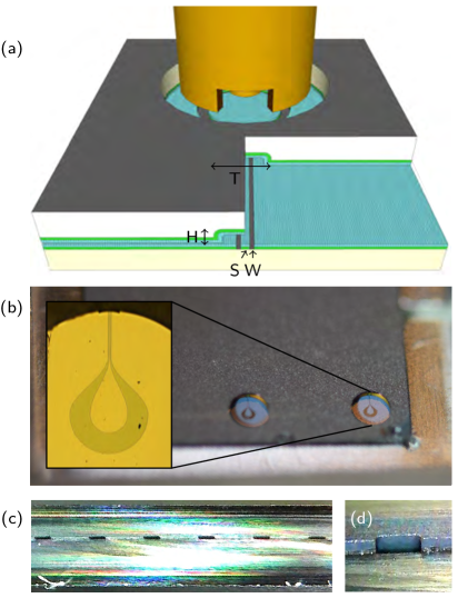
Figure 1 (a) illustrates the geometric characteristics of a capped device. The base chip consists of an intrinsic silicon substrate of thickness coated by an aluminum film with thickness followed by an indium film of equal thickness. These films are sputtered in situ in an ATC-Orion 5 sputter system from AJA International, Inc. The coplanar waveguide (CPW) transmission line visible in Fig. 1 (a) and other on-chip structures are defined by optical lithography followed by a wet-etch in Transene A aluminum etchant. 111We find that Transene A works well to etch indium thin films as well as aluminum.
The cap consists of a thick silicon wafer with tunnels trenched by isotropic reactive-ion etching (RIE) and through holes formed using a deep RIE process. After etching, the cap underside is metallized with the same aluminum-indium process as the base chip.
The bonding procedure is realized in a custom-made vacuum chamber with the aid of an aligning and compressing fixture (see details in the supplementary material). The base chip and cap are aligned with a horizontal accuracy of less than , significantly smaller than the device’s maximum allowed tolerances. The chips are subsequently compressed by applying vertical pressure with the fixture lid. At a system pressure of approximately , the chamber is placed for on a hot plate at , above the indium melting temperature (). Heating in vacuum prevents the formation of thick indium oxide Schoeller et al. (2006) and results in a strong mechanical bond without chemical or physical cleaning of the indium films prior to bonding. In fact, we found that bonded samples can withstand several minutes of high-power sonication and multiple cooling cycles to and . Images of a bonded device are shown in Figs. 1 (b), 1(c), and 1(d).
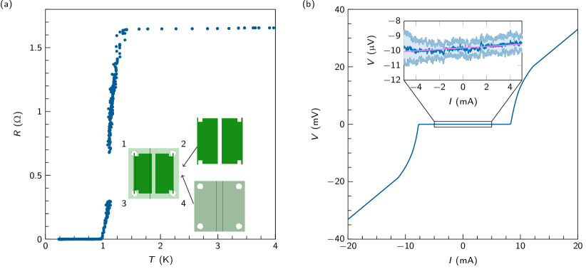
The dc electrical behavior of a bonded device is characterized using the base chip and cap layouts shown in the inset of Fig. 2. 222This design guarantees that a dc current flows through the indium bond and the metallized tunnel when measuring the resistance between the two base-chip islands. By applying a dc current through ports and and measuring the voltage across ports and , we find a room temperature dc resistance . This resistance is due to the room temperature resistance of the aluminum-indium films on both the base chip and cap as well as the bond resistance between the two chips. We realize detailed numerical simulations of the device under test (DUT) by means of ANSYS Q3D Extractor 333http://www.ansys.com/Products/Electronics/ANSYS-Q3D-Extractor and find a theoretical . The discrepancy between the measured and simulated resistance is likely due to the bond resistance (not included in the Q3D model), bond inhomogeneity, or both; possible contributors to these effects are the presence of native indium oxide before bonding, inter-diffusion of aluminum and indium, or a tilt between base chip and cap.
Bond inhomogeneity can be understood by modeling the five metallic layers of a bonded device – aluminum, indium, bond region, indium, and aluminum – as a large set of flux tubes directed from the base chip to the cap. At room temperature, each tube has a resistance ; the total resistance is approximately the parallel resistance of all flux tubes. Flux tubes in an unbonded region are open circuits with resistance and cause to increase. Following this model, the ratio between measured and simulated resistance indicates that approximately of the DUT is bonded. This result is verified by breaking apart bonded devices and inspecting optically the surfaces of the bond region (see supplementary material).
Figure 2 (a) shows a four-point measurement of as a function of temperature for the bonded device shown in the inset. Below the superconducting transition temperature of aluminum, , is approximately the bond resistance. The data points in the figure are obtained by measuring the device’s current-voltage (I-V) characteristic curves at various temperatures and fitting their slope. Figure 2 (b) shows the I-V curve measured at . We find a critical current intensity for the aluminum-indium films, . An ensemble of measurements well below is reported in the inset of Fig. 2 (b). From the least-squares best fit, we obtain a bond resistance , which is less than approximately assuming a bond area. This resistance is likely due to the native indium oxide film initially present on the chips, preventing the bond region from becoming superconductive at low temperatures.
Figure 3 displays the microwave characterization of three capped and uncapped devices with layouts shown in the insets. The measurements are realized by means of a vector network analyzer (VNA) from Keysight Technologies Inc., model PNA-X N5242A; details on the measurement setups can be found in Béjanin et al. Béjanin et al. (2016)
The measurements in Fig. 3 (a) demonstrate that the bonding process and the addition of the cap – including the tunnel mouth – do not noticeably increase reflections, which are instead dominated by the three-dimensional wires. Béjanin et al. (2016)
Figure 3 (b) shows a measurement of the isolation coefficient between two adjacent transmission lines (see inset). At microwave frequencies a signal injected at port or can leak to ports and , generating signal crosstalk. Due to the three-dimensional wires, signal crosstalk for the uncapped device is already very low. Béjanin et al. (2016) The cap further reduces crosstalk by more than across the entire measurement bandwidth. These results may have important implications to quantum computing, where crosstalk has been identified as a major source of error. Najafi-Yazdi, Kelly, and Martinis (2017)
Reflection and isolation measurements are performed at room temperature in order to maintain the DUT reference planes as close as possible to the VNA ports. However, the line shown in the inset of Fig. 3 (c) is characterized by a room-temperature loss sufficiently large to mask any abnormalities in transmission measurements at microwave frequencies. We therefore measure this line at , where both the indium and aluminum films are in the superconducting state.
Figure 3 (c) shows clean transmission for both uncapped and capped devices up to . At higher frequencies, we observe a series of pronounced resonances in the transmission coefficient of the capped device. The simulations in Fig. S3 of the supplementary material and the results in Fig. 3 (a) indicate that these resonances are not due to the presence of the tunnel. We believe they are caused by bond inhomogeneity, shown in Fig. S2 of the supplementary material, resulting in unwanted resonances similar to the slotline modes observed by Wenner et al. Wenner et al. (2011)
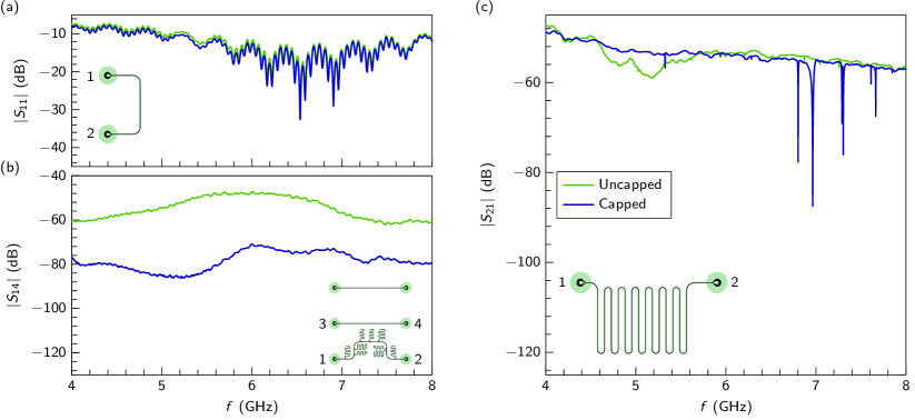
As a proof of concept for quantum computing applications, we fabricate and measure a set of capped superconducting CPW resonators. The device layout is sketched in the inset of Fig. 3 (b), which shows nine -wave resonators coupled to line in a multiplexed design. Béjanin et al. (2016)
The resonators are characterized by measuring their internal quality factor at and for a mean photon occupation number , similar to the excitation power used in quantum computing operations. The main resonator parameters are reported in Table 1. 444Five of the nine capped resonators were damaged during fabrication and, thus, their parameters are not reported in Table 1. The fits for the last two capped resonators in the table are poor; the corresponding quality factors are not shown. The measured data and fits for the second pair of resonators in Table 1 are shown in Fig. S4 of the supplementary material. Note that the resonance frequency of an uncapped resonator shifts with the addition of the cap.
In the supplementary material, we determine that the internal quality factor of a capped resonator is approximately larger than that of an uncapped resonator due to the vacuum participation. However, this effect is significantly smaller than the quality factor fluctuations over time 555By measuring a resonator over a time period of ten hours, we found a standard deviation as large as half of the mean quality factor. Neill et al. (2013) and, thus, it cannot be resolved in our measurements. In fact, accounting for time fluctuations, the quality factors for capped and uncapped resonators in Table 1 are approximately equal.
| () | () | |||
|---|---|---|---|---|
In conclusion, we have developed and characterized a hot thermocompression bonding technology in vacuum using indium thin films as bonding agent. Our results show that this technology can be readily used to implement an integrated multilayer architecture, combining the fabrication advantages of two-dimensional superconducting qubits Clarke and Wilhelm (2008) and the long coherence of micromachined three-dimensional cavities. Brecht et al. (2015) This bonding technology is compatible with the quantum socket design, paving the way toward the implementation of extensible quantum computing architectures as proposed by Béjanin et al. Béjanin et al. (2016)
In future implementations, we will improve the bonding procedure by including a cleaning step with an acid buff to remove native indium oxide prior to bonding. Additionally, we will use slightly thicker indium films (), a lower bonding pressure (), in vacuo chip alignment and compression, as well as a higher and more homogeneous compression by means of an hydraulic press. Finally, we will add an inter-diffusion barrier between the aluminum and indium films.
See supplementary materials for details on the thermocompression bonding setup, bond inhomogeneity, transmission simulations, resonator data and fits, and vacuum participation.
We acknowledge the Natural Sciences and Engineering Research Council of Canada and the Canadian Microelectronics Corporation Microsystems. We thank the Quantum NanoFab Facility at the University of Waterloo as well as the Toronto Nanofabrication Centre for their support with device fabrication, as well as F. Deppe and J.Y. Mutus for fruitful discussions.
References
- Ladd et al. (2010) T. D. Ladd, F. Jelezko, R. Laflamme, Y. Nakamura, C. Monroe, and J. L. O’Brien, “Quantum computers,” Nature 464, 45–53 (2010).
- Monz et al. (2011) T. Monz, P. Schindler, J. T. Barreiro, M. Chwalla, D. Nigg, W. A. Coish, M. Harlander, W. Hänsel, M. Hennrich, and R. Blatt, “14-qubit entanglement: Creation and coherence,” Physical Review Letters 106, 130506 (2011).
- Kelly et al. (2015) J. Kelly, R. Barends, A. G. Fowler, A. Megrant, E. Jeffrey, T. C. White, D. Sank, J. Y. Mutus, B. Campbell, Y. Chen, Z. Chen, B. Chiaro, A. Dunsworth, I.-C. Hoi, C. Neill, P. J. O’Malley, C. Quintana, P. Roushan, A. Vainsencher, J. Wenner, A. N. Cleland, and J. M. Martinis, “State preservation by repetitive error detection in a superconducting quantum circuit,” Nature 519, 66–69 (2015).
- Martinis (2015) J. M. Martinis, “Qubit metrology for building a fault-tolerant quantum computer,” npj Quantum Information 1, 15005 (2015).
- Jones et al. (2012) N. C. Jones, R. V. Meter, A. G. Fowler, P. L. McMahon, J. Kim, T. D. Ladd, and Y. Yamamoto, “Layered architecture for quantum computing,” Phys. Rev. X 2, 031007 (2012).
- Monroe and Kim (2013) C. Monroe and J. Kim, “Scaling the ion trap quantum processor,” Science 339, 1164–1169 (2013).
- O’Gorman et al. (2016) J. O’Gorman, N. H. Nickerson, P. Ross, J. J. Morton, and S. C. Benjamin, “A silicon-based surface code quantum computer,” npj Quantum Information 2, 15019 (2016).
- Lekitsch et al. (2017) B. Lekitsch, S. Weidt, A. G. Fowler, K. Mølmer, S. J. Devitt, C. Wunderlich, and W. K. Hensinger, “Blueprint for a microwave trapped ion quantum computer,” Science 3, 1–11 (2017).
- Clarke and Wilhelm (2008) J. Clarke and F. K. Wilhelm, “Superconducting quantum bits,” Nature 453, 1031–1042 (2008).
- Boixo et al. (2017) S. Boixo, S. V. Isakov, V. N. Smelyanskiy, R. Babbush, N. Ding, Z. Jiang, M. J. Bremner, J. M. Martinis, and H. Neven, “Characterizing quantum supremacy in near-term devices,” (2017), arXiv:1608.00263 .
- Gottesman (2010) D. Gottesman, “An introduction to quantum error correction and fault-tolerant quantum computation,” Quantum Information Science and Its Contributions to Mathematics, Proceedings of Symposia in Applied Mathematics 68, 13–58 (2010).
- Fowler et al. (2012) A. G. Fowler, M. Mariantoni, J. M. Martinis, and A. N. Cleland, “Surface codes: Towards practical large-scale quantum computation,” Phys. Rev. A 86, 032324 (2012).
- Córcoles et al. (2015) A. D. Córcoles, E. Magesan, S. J. Srinivasan, A. W. Cross, M. Steffen, J. M. Gambetta, and J. M. Chow, “Demonstration of a quantum error detection code using a square lattice of four superconducting qubits,” Nature Communications 6, 6979 (2015).
- Ristè et al. (2015) D. Ristè, S. Poletto, M.-Z. Huang, A. Bruno, V. Vesterinen, O.-P. Saira, and L. DiCarlo, “Detecting bit-flip errors in a logical qubit using stabilizer measurements,” Nature Communications 6, 6983 (2015).
- Ofek et al. (2016) N. Ofek, A. Petrenko, R. Heeres, P. Reinhold, Z. Leghtas, B. Vlastakis, Y. Liu, L. Frunzio, S. M. Girvin, L. Jiang, M. Mirrahimi, M. H. Devoret, and R. J. Schoelkopf, “Extending the lifetime of a quantum bit with error correction in superconducting circuits,” Nature 536, 441–445 (2016).
- Brecht et al. (2016) T. Brecht, W. Pfaff, C. Wang, Y. Chu, L. Frunzio, M. H. Devoret, and R. J. Schoelkopf, “Multilayer microwave integrated quantum circuits for scalable quantum computing,” npj Quantum Information 2, 16002 (2016).
- Brecht et al. (2015) T. Brecht, M. Reagor, Y. Chu, W. Pfaff, C. Wang, L. Frunzio, M. H. Devoret, and R. J. Schoelkopf, “Demonstration of superconducting micromachined cavities,” Appl. Phys. Lett. 107, 192603 (2015).
- Brecht et al. (2017) T. Brecht, Y. Chu, C. Axline, W. Pfaff, J. Z. Blumoff, K. Chou, L. Krayzman, L. Frunzio, and R. J. Schoelkopf, “Micromachined integrated quantum circuit containing a superconducting qubit,” (2017), arXiv:1611.02166 .
- O’Brien et al. (2017) W. O’Brien, A. Bestwick, M. Vahidpour, J. T. Whyland, J. Angeles, D. Scarabelli, M. Villiers, M. Curtis, A. Polloreno, M. Selvanayagam, A. Papageorge, N. Rubin, and C. Rigetti, “Engineering signal integrity in multi-qubit devices: Part i,” (2017), C46.00011 .
- Rosenberg et al. (2017) D. Rosenberg, D. Kim, D.-R. Yost, J. Mallek, J. Yoder, R. Das, L. Racz, D. Hover, S. Weber, A. Kerman, and W. Oliver, “3D integration for superconducting qubits,” (2017), H46.00001 .
- Kelly et al. (2017) J. Kelly, J. Mutus, E. Lucero, B. Foxen, R. Graff, P. Klimov, Z. Chen, B. Chiaro, A. Dunsworth, C. Neill, C. Quintana, J. Wenner, and J. M. Martinis, “3D integration of superconducting qubits with bump bonds: Part 2,” (2017), H46.00007 .
- Chen et al. (2014) Z. Chen, A. Megrant, J. Kelly, R. Barends, J. Bochmann, Y. Chen, B. Chiaro, A. Dunsworth, E. Jeffrey, J. Y. Mutus, P. J. J. O’Malley, C. Neill, P. Roushan, D. Sank, A. Vainsencher, J. Wenner, T. C. White, A. N. Cleland, and J. M. Martinis, “Fabrication and characterization of aluminum airbridges for superconducting microwave circuits,” Applied Physics Letters 104, 052602 (2014).
- Versluis et al. (2016) R. Versluis, S. Poletto, N. Khammassi, N. Haider, D. J. Michalak, A. Bruno, K. Bertels, and L. DiCarlo, “Scalable quantum circuit and control for a superconducting surface code,” (2016), arXiv:1612.08208 .
- Béjanin et al. (2016) J. Béjanin, T. McConkey, J. Rinehart, C. Earnest, C. McRae, D. Shiri, J. Bateman, Y. Rohanizadegan, B. Penava, P. Breul, S. Royak, M. Zapatka, A. Fowler, and M. Mariantoni, “Three-dimensional wiring for extensible quantum computing: The quantum socket,” Physical Review Applied 6 (2016), 10.1103/PhysRevApplied.6.044010.
- Note (1) We find that Transene A works well to etch indium thin films as well as aluminum.
- Schoeller et al. (2006) H. Schoeller, J. Kim, S. Park, and J. Cho, “Thermodynamics and kinetics of oxidation of pure indium solders,” MRS Proceedings 968 (2006), 10.1557/PROC-0968-V03-07.
- Note (2) This design guarantees that a dc current flows through the indium bond and the metallized tunnel when measuring the resistance between the two base-chip islands.
- Note (3) http://www.ansys.com/Products/Electronics/ANSYS-Q3D-Extractor.
- Najafi-Yazdi, Kelly, and Martinis (2017) A. Najafi-Yazdi, J. Kelly, and J. Martinis, “High fidelity, numerical investigation of cross talk in a multi-qubit xmon processor,” (2017), C46.00009 .
- Wenner et al. (2011) J. Wenner, M. Neeley, R. C. Bialczak, M. Lenander, E. Lucero, A. D. O’Connell, D. Sank, H. Wang, M. Weides, A. N. Cleland, and J. M. Martinis, “Wirebond crosstalk and cavity modes in large chip mounts for superconducting qubits,” Superconductor Science and Technology 24, 065001 (2011).
- Note (4) Five of the nine capped resonators were damaged during fabrication and, thus, their parameters are not reported in Table 1. The fits for the last two capped resonators in the table are poor; the corresponding quality factors are not shown.
- Note (5) By measuring a resonator over a time period of ten hours, we found a standard deviation as large as half of the mean quality factor. Neill et al. (2013).
- Neill et al. (2013) C. Neill, A. Megrant, R. Barends, Y. Chen, B. Chiaro, J. Kelly, J. Y. Mutus, P. J. J. O’Malley, D. Sank, J. Wenner, T. C. White, Y. Yin, A. N. Cleland, and J. M. Martinis, “Fluctuations from edge defects in superconducting resonators,” Applied Physics Letters 103, 072601 (2013).
Supplementary Materials for “Thermocompression Bonding Technology for Multilayer Superconducting Quantum Circuits”
In this supplementary materials, we provide further details on the thermocompression bonding setup. We characterize bond inhomogeneity with optical imaging. We present numerical simulations of the transmission coefficient at microwave frequencies for various configurations of capped and uncapped coplanar waveguide (CPW) transmission lines. We show the measured data and fits for a capped and uncapped superconducting resonator at . Finally, we calculate the ratio of the internal quality factor for a capped and uncapped resonator, thus estimating the effect of vacuum participation.
S1: THERMOCOMPRESSION BONDING SETUP AND PROCEDURE
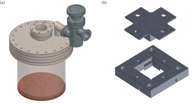
Figure S1 shows a computer-aided design of the custom-made vacuum chamber and aligning-compressing fixture used for the thermocompression bonding. The bottom of the chamber is made from a thick copper plate, ensuring a high thermal conductivity and heat capacity. The bottom surface of the plate is mirror polished each time before placing the chamber on the hot plate. The top surface features a set of threaded screw holes, where aligning-compressing fixtures with different dimensions can be fixed; the chamber is designed to process up to -in. wafers. The chamber’s wall is a high, thick hollow cylinder made from stainless steel, the low thermal conductivity of which ensures little or no heating of the top part of the chamber. The top edge of the cylindrical wall is welded to a -in. ConFlat (CF) flange made from 304L stainless steel. 666A new chamber is being designed made from 316LN stainless steel with low magnetic permeability , reducing magnetic contamination of the samples. The CF flange features a knife-edge seal mechanism; the sealing element is a fully annealed copper gasket. The gasket is made from hard, high purity, oxygen-free (OFHC) copper, which allows for system pressures as low as at operating temperatures up to . A ultra-high vacuum, temperature-resistant valve is used to connect the CF flange to a pump. A CF flanged Kodial glass viewport (sealed with a silver plated copper gasket) permits the observation of the chamber’s interior during processing.
The aligning-compressing fixture is a square washer with inner dimensions made from stainless steel and featuring an adjustable edge corner. This corner can be moved along a groove at the bottom of the washer, allowing alignment between the base chip and cap. In this work, we use square chips with dimensions . Note that the base chip is in direct contact with the copper plate, guaranteeing good thermalization. The aligning procedure comprises three steps: First, the base chip is placed inside the washer at the bottom of the chamber and pushed against the washer’s corner opposite to the adjustable corner; second, the cap is manually dropped on the base chip, pre-aligning the chips as accurately as possible; third, the two chips are aligned with the adjustable corner, which is finally fixed to the chamber with a screw. The manual pre-alignment in step two is sufficient to prevent damage of the on-chip structures due to relative dragging of the chips during step three. The lid shown in Fig. S1 (b) is used to apply pressure on the aligned chips by means of four screws. We find that little pressure is required to obtain a mechanically strong bond.
After closing the chamber, we evacuate it with a molecular pump from Pfeiffer Vacuum GmbH for to reach a system pressure of . While pumping we monitor the chamber leak rate, which is typically on the order of . Once the chamber is placed on the hot plate, the temperature initially fluctuates reaching a steady state in approximately ; at that time we start counting . Pumping is continued during the entire heating process, as well as during a cooling period when the chamber is placed to rest on a thick aluminum plate.
Our bonding procedure is simple and highly reproducible, with a yield of for a total of bonded samples.
When performing thermocompression bonding of devices with superconducting qubits, the Josephson tunnel junctions that make the qubits will be heated at high temperature. In order to verify whether this process damages the Josephson junctions, we fabricate a set of aluminum-aluminum oxide-aluminum junctions using e-beam lithography and evaporation. The junctions’ area is and their room temperature resistance . We perform a preliminary test by heating the junctions to for at atmospheric pressure, finding that most of the junctions survive the process. In addition, we find that the post-heat room temperature resistance decreases to approximately . A complete study of heating effects on submicron sized Josephson junctions was performed by Koppinen et al. Koppinen, Väistö, and Maasilta (2006) By heating the junctions up to in high vacuum (less than ), the authors found a stabilization of the junctions’ tunneling resistance as well as a reduction of the junctions’ rate of aging. These results are very encouraging, indicating that the hot bonding process may even improve the quality of the Josephson junctions.
S2: BOND INHOMOGENEITY
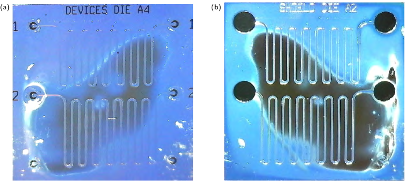
Bond inhomogeneity can be characterized by breaking apart a bonded device and imaging the base chip and cap bond surfaces optically, as shown in Fig. S2. The images refer to the device outlined in the inset of Fig. 3 (c) in the main text and are taken by means of a handheld digital microscope.
The indium film within the boundary of the through holes on the base chip [see Fig. S2 (a)] is heated during the bonding process, but not bonded to the cap. We can thus use the color of the indium film in this region as a reference to discern bonded from not bonded regions. We determine that the region near the center of the base chip and cap was bonded well, whereas the area around the edges of the two chips was not bonded. In this case, approximately of the chips’ area was bonded well. We find similar results in other devices. This effect is likely due to the compressing fixture lid that was designed to be smaller than the chips’ area, thus applying pressure only to the center of the chips. In the conclusions of the main text we propose a remedy to this issue.
S3: TUNNEL MOUTH MICROWAVE SIMULATIONS
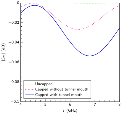
The edge of a through hole where the cap tunnel begins (the tunnel mouth) represents a boundary condition for the electromagnetic field associated with a capped transmission line. The line shown in the inset of Fig. 3 (c) in the main text is characterized by two of such boundary conditions. In order to determine whether these conditions generate unwanted resonance modes, we simulate the transmission coefficient for this line and compare it to that of an uncapped line and of a capped line without tunnel mouths (i.e., covered by an infinitely long tunnel). The numerical simulations are performed with ANSYS HFSS, 777http://www.ansys.com/products/electronics/ansys-hfss assuming perfect conductors and lossless CPW transmission lines with equal geometric characteristics.
The graphs displayed in Fig. S3 reveal almost perfect transmission for the three simulated configurations, with less than of loss due to slight impedance mismatch. We can safely conclude that the unwanted resonances shown in Fig. 3 (c) of the main text are not due to the presence of the tunnel mouths.
S4: CAPPED SUPERCONDUCTING CPW RESONATORS
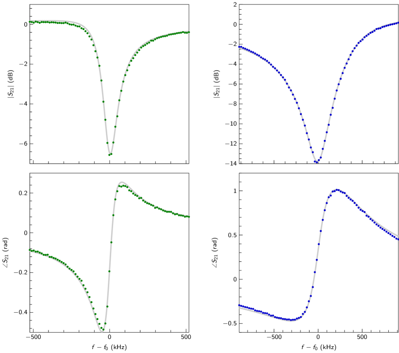
Figure S4 shows data and fits for the second pair of uncapped and capped superconducting resonators reported in Table 1 of the main text. The displayed data for the capped resonator is the ensemble average of measured traces, whereas only one trace is measured for the uncapped resonator. In both cases, each data point is obtained setting the vector network analyzer (VNA) to an intermediate frequency bandwidth .
S5: VACUUM CONTRIBUTION TO CAPPED RESONATORS QUALITY FACTOR
In this section, we estimate the effect of a metallized cap on the internal quality factor of a superconducting CPW transmission line resonator. The addition of a grounded cap above a CPW resonator forces some of the electric field lines to be distributed from the base chip to the cap, away from the base chip substrate. This increases the contribution of vacuum to the mode volume of a capped resonator compared to the case of an uncapped resonator. Assuming all metallic structures to be perfect conductors, the internal quality factor is solely due to dielectric losses and, thus, it can be found by inverting the loss tangent as, Simons (2001)
| (1) |
where is the effective electric complex permittivity of the CPW transmission line with real and imaginary parts and , respectively ().
The effective electric permittivity of a capped CPW transmission line can be calculated using Eq. (2.39) in Simons Simons (2001)
| (2) |
where is the partial filling factor dependent on the device geometry [see Eq. (2.40) in Simons Simons (2001)] and is the relative electric complex permittivity of the base chip substrate (in our case silicon) with thickness . Hereafter, we assume (a reasonable approximation as the silicon substrates are thick, much thicker than any of the other structures; see main text for all relevant dimensions). Note that Eq. (2) is applicable as the tunnel sidewalls are much farther away from the conductor than the in-plane ground planes, (see Fig. 1 in the main text).
In the case of an uncapped CPW transmission line, the effective electric permittivity is given by Simons (2001)
| (4) |
and the internal quality factor is given by
| (5) |
The ratio between the uncapped and capped internal quality factors is thus
| (6) |
Using the dimensions , , and reported in the main text and assuming for silicon, we find and, thus, . As a consequence, the increase in vacuum participation due to the addition of the cap increases the internal quality factor by approximately . This is a very small effect for the devices presented in this work, where other loss mechanisms such as the presence of native indium oxide on both the base chip and cap, the low quality thin-film sputter deposition, and possibly the bonding procedure itself outweigh the benefits of a higher vacuum participation. However, a careful design and a suitable fabrication and cleaning process may be used to take advantage of this effect to make capped devices (e.g., qubits) with lower error rates than similar uncapped devices.
References
- Note (1) A new chamber is being designed made from 316LN stainless steel with low magnetic permeability , reducing magnetic contamination of the samples.
- Koppinen, Väistö, and Maasilta (2006) P. J. Koppinen, L. M. Väistö, and I. J. Maasilta, “Effects of annealing to tunnel junction stability,” AIP Conference Proceedings 850, 1639–1640 (2006).
- Note (2) http://www.ansys.com/products/electronics/ansys-hfss.
- Béjanin et al. (2016) J. Béjanin, T. McConkey, J. Rinehart, C. Earnest, C. McRae, D. Shiri, J. Bateman, Y. Rohanizadegan, B. Penava, P. Breul, S. Royak, M. Zapatka, A. Fowler, and M. Mariantoni, “Three-dimensional wiring for extensible quantum computing: The quantum socket,” Physical Review Applied 6 (2016), 10.1103/PhysRevApplied.6.044010.
- Simons (2001) R. N. Simons, Coplanar Waveguide Circuits, Components, and Systems (John Wiley & Sons, Inc., Hoboken, NJ, USA, 2001).