MOVPE growth, transmission electron microscopy and magneto-optical spectroscopy of individual InAsxP1-x/Ga0.5In0.5P quantum dots
Abstract
We report on growth and characterization of individual InAsxP1-x/GaInP quantum dots with variable nominal As molar fraction. Magneto-photoluminescence experiments reveal QD emission in a wide range from 1.3 to 1.8 eV confirming incorporation of As into quantum dots. Transmission electron microscopy reveals a core-cap structure of InAsP quantum dots with an InAs-rich core capped by an InP-rich layer. Inside the core, an As molar fraction up to =0.12 is observed. The heavy hole -factor is found to be strongly dependent on As molar fraction, while the electron -factor is close to the InP values. This suggests type-II carrier confinement in the studied InAsP dots with holes (electrons) localized in the core (cap) region. Finally, dynamic nuclear polarization is observed which allows for further insight into structural properties using nuclear magnetic resonance.
I Introduction
Semiconductor quantum dots (QDs) play a crucial role in emerging semiconductor device technologies such as single photon sources and detectors, quantum memories and logic gates Bimberg and Pohl (2011). Their electronic properties can be tailored by modifying their size and composition. For example, electronic properties of QDs can be engineered using ternary alloys. In this context, ternary IIIxIII1-xV QD systems have received most attention. Self-assembled Stranski-Krastanov InxGa1-xAs/GaAs quantum dots are the most studied system, in which the alloy composition and dot size can be modified to obtain a broad range of emission energies Sugawara (1999); Bimberg and Kirstaedter (1997); Shumway et al. (2001).
On the other hand, ternary III VxV1-x Stranski-Krastanov QDs have not been studied in detail. InAsxP1-x QDs grown by self-assembly in Ga0.5In0.5P is the system considered in the present work. Due to the significant difference between the bandgaps of InAs and Ga0.5In0.5P (1.5 eV at room temperature), a pronounced increase in confinement energy can be expected for InAsP/GaInP QDs compared to InP/GaInP QDs, favouring robust performance of QDs at elevated temperatures. The first report on Stranski-Krastanow growth of InAsP QDs in GaInP by metalorganic vapour phase epitaxy (MOVPE) was published by Vinokurov et al. Vinokurov and Kapitonov (1998). However, no significant red-shift of luminescence was observed compared to InP QDs which could be a result of either inefficient As incorporation into QDs, or the reduction of QD sizes under As incorporation. By contrast, Fuchi et al. have grown InAsP QDs using droplet hetero-epitaxy technique and observed a significant red-shift and broadening of the ensemble QD emission with increased As fraction Fuchi et al. (2008). Ribeiro et al. reported experiments on InAsP/GaAs structures, where quantum dot emission at 77 K was found to be around 1.25 eV , which lies above the emission energy of InAs/GaAs measured under the same conditions Ribeiro and Maltez (2002). In the work of Ribeiro et al. the electronic properties of InAsP/GaAs QDs were controlled by the PH3 flux during the MOVPE process: as the flux was increased, the QD emission energy increased towards the InP QD energy Maltez and Ribeiro (2003). In our work we follow a similar approach and use the flux of AsH3 to control the QD properties. Some recent examples of QD growth using ternary InAsP alloy also include demonstration of the InAsP QD lasers Karomi et al. (2015); Krysa et al. (2016) and observation of ultraclean emission from InAsP QDs embedded in InP nanowires Dalacu et al. (2012).
To the best of our knowledge, here we present the first report on growth, transmission electron microscopy and magneto-optical studies of individual InAsP/GaInP quantum dots, which offer deeper confinement potential energies compared to the previously studied InP/GaInP and InAsP/GaAs QDs. Magneto-photoluminescence (magneto-PL) studies reveal detailed information of the electron and hole -factor dependence on quantum dot emission energy which varies in a wide range between 1.3 and 1.8 eV. Such knowledge of the -factors is key for development of technologies that employ QD spins Kosaka and Kiselev (2001); van Bree et al. (2012); Witek et al. (2011). A combination of results from magneto-PL and transmission electronic microscopy (TEM) imaging suggests type-II carrier confinement in the studied InAsxP1-x QDs with sufficiently large As molar fraction . Recently, type-II QDs have attracted considerable attention as potential candidates for efficient QD solar cells due to their increased carrier lifetime and suppressed Auger recombination Kim et al. (2003); Laghumavarapu et al. (2007); Ning et al. (2011); Tayagaki and Sugaya (2016).
II Samples and experimental methods
Our samples of ternary InAsxP1-x QDs embedded in Ga0.5In0.5P matrix, were grown by low pressure (150 Torr) MOVPE in a horizontal flow reactor, on (100) GaAs substrates with a miscut angle of 3∘ towards (10). Trimethylgallium (TMGa) and Trimethylindium (TMIn) were used as precursors for group III elements, and arsine (AsH3) and phosphine (PH3) were used as precursors of group V. Hydrogen was used as carrier gas. The GaAs buffer layer and the subsequent GaInP barrier were grown at 690∘C. The growth rates were maintained at 0.76 nm/s for the GaAs buffer layers and GaInP barriers. QDs were deposited at a lower nominal growth rate of 0.11 nm/s. During the growth of the GaInP barriers and quantum dots the PH3 flow was kept constant at 300 sccm, while the composition of the InAsP QDs was controlled by the flow rate of AsH3. Before the deposition of the QDs, the growth was halted, and the susceptor temperature was lowered to 650∘C. The growth of the QDs included three steps: The first step involved deposition of a nominally binary InP for 1 s, this was followed by InAsP deposition for 3 s during which arsine was introduced to the reactor, finally a nominally binary InP was grown again for 1 s. The sample with pure InP/GaInP dots (0 sccm arsine flux) was produced by growing InP for 5 s in a single step. In what follows we label the samples by the arsine flux used during the dot growth.
In order to assess the nominal molar fractions of arsenic in QDs grown with different AsH3 flows, four InAsP/InP superlattice (SL) samples have been grown on InP substrates under the same growth conditions as for QD structures. The growth times of the InAsP layers were 5 s or 10 s and the total growth times of one complete SL period were 60 s or 120 s, respectively. The SL structures were examined by means of X-ray diffractometry as described in Krysa et al. (2016). The molar fractions were derived from the position of the zero order SL peak with respect to the peak from the InP substrate. The resulting arsenic molar fractions in the InAsP layers are 0.06, 0.072, 0.084, and 0.108 for AsH3 flows of 5.9 sccm, 10.6 sccm, 16.7 sccm, and 20.2 sccm respectively.
Optical characterization of QDs was carried out using a micro-photoluminescence (PL) setup equipped with a confocal low-temperature optical microscope system. An external magnetic field up to 10 T parallel (Faraday geometry) or perpendicular (Voigt geometry) to the sample growth axis was applied using a superconducting magnet. In most experiments PL was excited using either HeNe laser ( eV) or diode laser ( eV), with additional diode lasers ( eV, eV) used for experiments on nuclear spin effects. Photoluminescence signal was collected with a 0.85 m double spectrometer and a liquid nitrogen cooled charge coupled device (CCD). All optical spectroscopy experiments were carried out at a sample temperature of 4.2 K. Microscopy characterisation of the QDs presented in section III.1 was conducted using a composition-sensitive high-resolution transmission electron microscopy (TEM), the details of this methods are described on Ref. Karomi et al. (2015).
III Results and discussion
III.1 Transmission Electron Microscopy
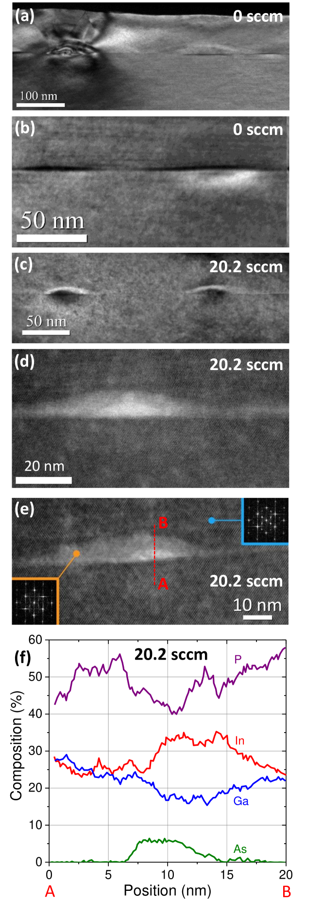
We carried out transmission electron microscopy (TEM) studies in order to examine the morphology and chemical composition of the quantum dots. Fig. 1(a) shows a conventional TEM image taken under 002 dark field conditions on a sample grown without As (0 sccm). Contrast in these images is sensitive to the difference in the mean atomic number of the group III and V superlattices. Two types of InP/GaInP quantum dots are observed; large pyramid-shaped dots (e.g. left side of the image) and smaller disk shaped dots (e.g. right side of the image). Further examples of disk shaped InP/GaInP dots are shown in Fig. 1 (b). Similar 002 dark field TEM images of InAsP/GaInP dots (20.2 sccm sample) are shown in Fig. 1(c). It is apparent that these InAsP dots are pyramid shaped and have smaller lateral dimensions of 40 nm as opposed to 80 nm for both types of InP dots in Figs. 1(a, b).
In order to examine the chemical composition, further studies on InAsP/GaInP dots (20.2 sccm sample) were conducted using aberration-corrected scanning TEM (AC-STEM). Representative images taken under annular dark field (ADF) conditions are shown in Figs. 1(d, e). In these images brighter areas correspond to elements with larger atomic number . It is apparent that a typical InAsP dot consists of a core containing heavy elements covered by a cap of lighter elements. The image is aligned with the (001) planes horizontal, showing the QD has formed preferentially in a local steepening of the 3∘ offcut surface. Cu-Pt type ordering in the InGaP matrix is evident from the fast Fourier transform (FFT) shown in top right box in Fig. 1(e); no such ordering is observed in the QD core or cap (FFT in bottom left box).
In order to quantify segregation of elements with different inside QDs, we have performed energy-dispersive X-ray analysis (EDX): the results of the scan along the dashed line for the quantum dot shown in Fig. 1(e) are presented in Fig. 1(f). It can be seen that the quantum dot consists of a bottom ”core” region that is rich in As and In (which substitute P and Ga of the Ga0.5In0.5P barrier respectively), and the top ”cap” region that is rich in In only. Taking the arsenic/phosphorus ratio in Fig. 1(f) we can estimate the arsenic fraction to be , which is in good agreement with derived from X-ray diffractometry on the reference superlattice sample grown with the same arsine flow rate of 20.2 sccm.
In summary, TEM imaging shows that the sample growth with AsH3 flow results in arsenic incorporated into quantum dots. The resulting InAsP dots have notably smaller lateral dimensions than InP dots and exhibit a core-cap structure, resembling the core-shell structure of colloidal dots Kim et al. (2003). As we show below, these findings agree with the measurements of diamagnetic shifts and carrier -factors in individual dots. Furthermore, we present experimental results that point to type-II confinement in such core-cap geometry with electrons localized in the InP-rich cap and and holes occupying the InAs-rich core.
III.2 Effect of arsenic incorporation on quantum dot photoluminescence
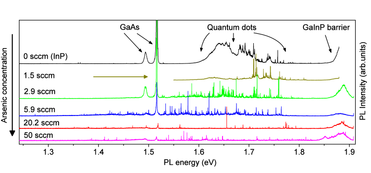
Figure 2 shows the PL spectra of six InAsP QDs samples grown with different nominal As concentrations. The spectra were measured in a wide range of energies (1.3 - 1.85 eV). The relative concentrations of As are given in terms of AsH3 flux in standard cubic centimeters per minute (sccm) on the left side of the graph. The top spectrum (black line) shows QD emission of the sample without arsenic (InP/GaInP). The spectrum is similar to those reported previously Elliott et al. (2010): the sharp peaks at 1.67 - 1.8 eV are attributed to the disk shaped quantum dots [see Fig. 1(b)], while broad emission features centered at 1.65 eV most likely originate from the large pyramidal quantum dots [see Fig. 1(a)]. When the AsH3 flux is increased (spectra from top to bottom) the spectral range of quantum dot emission peaks progressively widens, extending below the GaAs substrate emission at 1.52 eV for As concentrations above 2.9 sccm. The samples with the largest AsH3 flux (20.2 sccm and 50 sccm) exhibit single-dot emission in a wide range spanning from 1.3 to 1.8 eV. Importantly, there are quantum dots with emission energies below the bulk band gap of InP (1.421 eV at =4.2 K). Such pronounced shift of PL emission to lower energies is a clear sign that arsenic is incorporated into quantum dots.
It follows from the spectra of Fig. 2, that quantum dot PL intensity decreases with increasing arsenic concentration. As we explain later, we ascribe such behaviour to the transition from type-I to type-II carrier confinement for quantum dots with high arsenic concentration.
Even for the highest As fraction, the typical luminescence linewidths of the studies QDs are less than 50eV suggesting that As incorporation does not deteriorate the optical quality of the InAsP/InP dots.
III.3 Magneto-photoluminescence spectroscopy
In this section we present results of PL spectroscopy in external magnetic fields for quantum dot samples with different As concentration. Using these data we explore how electron and hole states are modified by incorporation of As into InP QDs. As we show, such studies also provide information on the chemical composition and structure of the InAsP QDs, complementary to TEM imaging.
III.3.1 Derivation of the quantum dot charge states and -factors
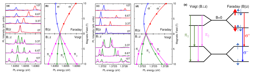
We first present magneto-PL spectroscopy data which reveals information on the charge states of the QDs. Two different geometries were used in our measurements: in Faraday (Voigt) geometry magnetic field is applied parallel (perpendicular) to the sample growth axis (). Figure 3(a) shows PL spectra of a single quantum dot in a sample with large As concentration (20.2 sccm) detected in two circular polarizations in Faraday geometry and in two orthogonal linear polarizations in Voigt geometry. Magnetic field dependence of the spectral positions of the peaks observed in Fig. 3(a) is shown in Fig. 3(b) by the symbols. Zeeman splitting and diamagnetic shift are observed both for and . In Faraday geometry the QD emission line splits into a circularly polarized ( and ) doublet, whereas in Voigt geometry a quadruplet of linearly polarized ( and ) lines is observed.
In order to describe the dependence of PL peak energies on magnetic field we use the following equations Bayer et al. (2002):
| (1) | |||||
| (2) |
where is the emission energy at , the Bohr magneton, and are the diamagnetic shifts in Faraday and Voigt geometry, ) is the exciton -factor in Faraday geometry, () is the heavy hole -factor along (perpendicular to) the sample growth axis, and electron -factor is assumed to be isotropic. We performed simultaneous least-square fitting of the data measured in Faraday (Voigt) geometry to Eq. 1 (Eq. 2). The fitting results for the data in Figs. 3(a,b) are shown by the lines in Fig. 3(b) and yield = +1.592, =+3.175, = +1.58, =0.737, =2.67 eV/T2 and =1.12 eV/T2. The same analysis is presented in Figs. 3(c,d) for another single dot from the same sample emitting at lower energy. Once again the data is well described by equations Eqs. 1-2 but with notable difference in -factors and diamagnetic shifts which is discussed in more detail in Subsections III.3.2 and III.3.3. Due to the signs in Eqs. 1-2 there is potential ambiguity in the signs of the fitted -factors. However, the signs of , are reliably established by comparing with the previous studies on neutral InP/GaInP quantum dotsChekhovich et al. (2010a) and bulk InPGotschy et al. (1989). By contrast the sign of is not defined and only the absolute value can be found from the fitting.
The patterns of spectral components in Figs. 3(a,c) as well as their good description within the model of Eqs. 1-2 prove that the observed emission arises from singly-charged quantum dots Bayer et al. (2002): In particular, in Voigt geometry, all four peaks maintain similar intensities and converge to the same energy in the limit of as opposed to the behaviour of ”dark” excitons in neutral quantum dots Bayer et al. (2002); Chekhovich et al. (2011a). The origin of two (four) spectral peaks in Faraday (Voigt) geometry is illustrated in Fig. 3(c) where spin states and optical transitions are shown schematically for a negatively charged exciton.
All narrow spectral peaks that have been examined, exhibit similar trion behaviour in all of the studied samples. This suggests that all of the studied dots emit from a charged state, which can be ascribed to the combined effect of background doping and optical excitation above the GaInP barrier bandgap. Distinguishing between positively and negatively singly charged dots using PL spectroscopy alone is difficult. However, we note that high magnetic field ( T) applied in Faraday geometry leads to unequal intensities of the two Zeeman PL components – a sign of relaxation between electron or hole spin Zeeman levels. We observe dots where both high- and low- energy peak becomes dominant in high field [compare Figs. 3(a,c)], suggesting that both positively and negatively charged quantum dots are encountered in the studied samples.
III.3.2 Effect of arsenic incorporation on diamagnetic shifts
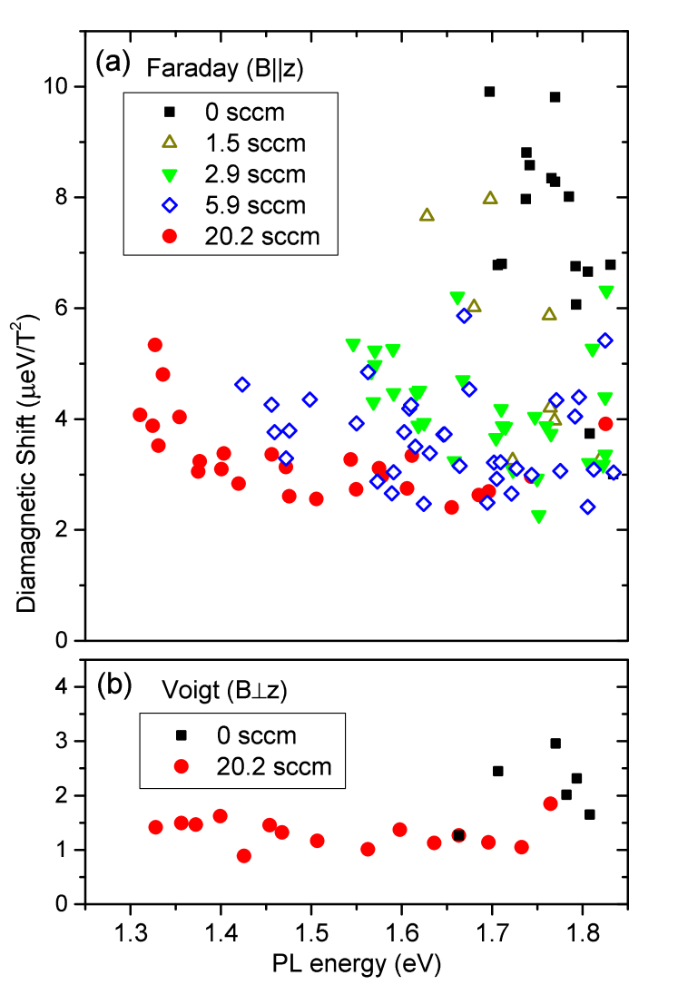
Measurements of exciton diamagnetic shifts and exciton -factors () have been carried out for 120 QDs that have been selected for relatively bright PL and narrow linewidths in five samples with different As concentration (AsH3 flux between 0 - 20.2 sccm). Figures 4(a) and (b) show the exciton diamagnetic shifts and measured in Faraday and Voigt geometries respectively. The measurements of and allow the effect of arsenic incorporation on quantum dot size and shape to be examined. The diamagnetic shift is related to the radius of the exciton wavefunction in the plane perpendicular to the external magnetic field by the following equation Walck and Reinecke (1998):
| (3) |
where is the electron charge and is the reduced exciton mass.
It can be seen in Fig. 4(a) that the largest diamagnetic shifts in Faraday geometry 8eV/T2 are observed for pure InP dots (0 sccm sample). Increased arsenic concentration results in reduced for the dots emitting at the same energies. This trend in diamagnetic shifts suggests that incorporation of arsenic into InAsP quantum dots results in reduction of their lateral dimensions. Such conclusion agrees with the TEM results presented in Section III.1. Furthermore in the sample with large As fraction (20.2 sccm) tends to increase for quantum dots with smaller emission energy suggesting their increased lateral dimensions. The diamagnetic shifts in Voigt geometry presented in Fig. 4(b) are notably smaller than agreeing with the disk-shape nature of the dots revealed by TEM.
III.3.3 Effect of arsenic incorporation on -factors and analysis of carrier confinement
In order to gain deeper insight into the spin properties of InAsP QDs, we extract the magnitudes of -factors for samples with different arsenic content. As we show below, these data provides useful information about quantum dot composition and structure and suggests type-II carrier confinement.
The symbols in Figure 5 show the out-of-plane exciton -factors measured in Faraday geometry as a function of the QD ground state emission energy in five samples. Linear fits are plotted by the lines to visualize the trends in exciton -factors for samples with different As compositions; the fitting parameters are listed in Table I. It can be seen from Fig. 5 that increased AsH3 flux leads to systematic increase in exciton -factors at all energies where QD luminescence is observed. Furthermore, the slopes of the dependencies decrease for large As concentration. These pronounced variations in signify the change in the chemical composition in the QD volume where exciton wavefunction is localized and thus confirm successful incorporation of As into the dots.
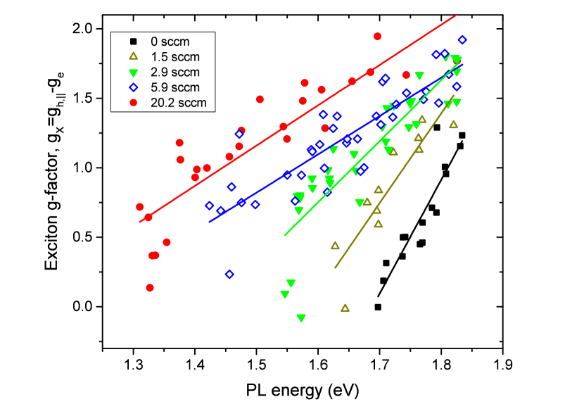
| Sample | m (eV-1) | at eV |
|---|---|---|
| 0 sccm | 8.18567 | 0.904 |
| 1.5 sccm | 6.459 | 1.381 |
| 2.9 sccm | 4.400 | 1.640 |
| 5.9 sccm | 2.758 | 1.640 |
| 20.2 sccm | 2.899 | 2.012 |
In order to gain further insight we examine the contributions of the electron and hole -factors to the variation of the exciton observed in Figure 5. For this purpose we focus on two samples with zero and large (20.2 sccm) arsenic concentration and conduct magneto-PL measurements where the same dots are measured both in Faraday and Voigt geometry allowing electron and hole -factors to be derived as described in Subsection III.2. Figure 6 shows the extracted -factors for the 0 sccm sample (open symbols) and the 20.2 sccm sample (solid symbols). The thin solid lines are linear fits which can be used as guides to an eye. We first note the large spread in the values, which is expected since heavy hole in-plane -factors depend strongly on the anisotropy of shape and strain of each particular dot Bayer et al. (2002). The results for out-of-plane heavy hole -factors and for electron -factors are more robust and show a striking difference: while values follow the same trend for both samples, there is a pronounced deviation in values. It is thus evident that it is the heavy-holes which are the most sensitive to incorporation of arsenic into the InAsP dots, whereas electrons have similar properties in structures with and without arsenic.
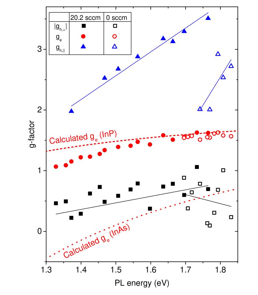
For quantitative analysis we use the result of Roth et al Roth et al. (1959) that electron -factor is determined mainly by the bandgap of the semiconductor. While it was derived originally for bulk materials this result has been extended successfully to quantum wells and quantum dots Sirenko et al. (1997); Yugova et al. (2007); Syperek et al. (2012). Thus we write for electron -factor:
| (4) |
where is the band gap, is the spin-orbit splitting and is the Kane energy parameter. (We use =0.38 eV, =21.11 eV for InAs and =0.11 eV, =17.0 eV for InP as reported in the literature Bastard (1991); Peter Y. Yu (2005).) Equation 4 is plotted in Fig. 6 by the dashed line for InP and by the dotted line for InAs. The simple theoretical equation is in excellent agreement with experimental values if we assume pure InP parameters. We thus conclude that both in InAsP and InP dots the electron behaves as if the dot consists of nearly pure InP, with small deviation developing only for the dots with the lowest ground state energy. While can not be calculated in a simple way, it is generally proportional to the and parameters of the valence band Lawaetz (1971) and can thus be expected to be larger for InAs than for InP. Therefore, the increase in observed for the 20.2 sccm sample in Fig. 6 is attributed to the increased fraction of arsenic ”sampled” by the hole wavefunction in the InAsP dots. To summarize, our observations strongly suggest that electrons and holes are localized in spatially separated parts of the quantum dot.
We propose the following interpretation that agrees with the observed -factor values, reduced luminescence intensity of QDs with large As concentration, and TEM results of Section III.1: The growth conditions favour the formation of core-cap QDs where InP-rich cap region localizes the electron and is separated from the InAs-rich core region where the hole is predominantly localized. Such spatial separation of electrons and holes may give rise to type-II QD behaviour. This conclusion is non-trivial since electronic band alignment at InAsP/InP interface is expected to be of type-I (Ref. Vurgaftman et al. (2001)). The most likely explanation is that large inhomogeneous strain characteristic of self-assembled QDs can lead to significant shift in energy levels Grundmann et al. (1995) and can be responsible for type-II band alignment.
Recently, type-II QDs have received increased attention as promising candidates for QD solar cells applications, where spatial separation of electrons and holes reduces spontaneous recombination and favours carrier extraction. Moreover, the structures studied here exhibit InAsP QDs with a broad range of the band-gap energies (from 1.3 eV to 1.8 eV) which could be advantageous for light conversion efficiency.
III.3.4 Optical control of the quantum dot nuclear spins
All isotopes of the elements present in InAsP/GaInP quantum dots have non-zero nuclear spins, as a result electron-nuclear interactions are significant Chekhovich et al. (2013); Urbaszek et al. (2013); Abragam (1961). Using circularly polarized optical excitation it is possible to inject spin-polarized electrons into quantum dot. Spin polarized electron can then transfer their polarization to one of the nuclear spins of the dot via the electron-nuclear hyperfine interaction. Repeated optical recombination and re-excitation of the spin polarized electrons can then lead to substantial polarization of the quantum dot nuclear spin ensemble, typically consisting of 105 nuclei. Such dynamic nuclear polarization (DNP) process has been reported previously for different types of quantum dots Gammon et al. (2001); Eble et al. (2006); Puebla et al. (2013) including InP/GaInP quantum dots Skiba-Szymanska et al. (2008); Chekhovich et al. (2010a, b, 2011b, 2011a). Here we extend these studies to InAsP/GaInP quantum dots.
The measurements were conducted on the 20.2 sccm sample in external magnetic field parallel to the sample growth direction (Faraday geometry). Magnetic field splits the QD emission peak into a Zeeman doublet [see Figs. 3(a,c)]. Since the two peaks of the spectral doublet originate from electron states with opposite spins [see Fig. 3(d)] the onset of nuclear spin polarization results in hyperfine (Overhauser) shift, i.e. increase or decrease of the Zeeman splitting depending on the direction of the effective nuclear field. (Here for simplicity we neglect the interaction of the hole spin with the nuclei since its contribution is at least 10 times smaller than that of the electronFallahi et al. (2010); Chekhovich et al. (2011b).)
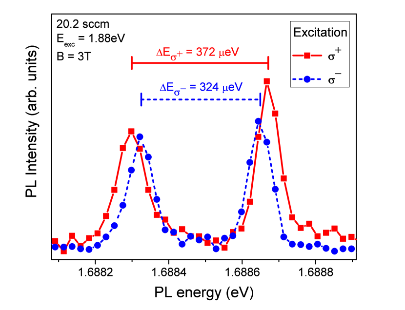
The change in induced by DNP can be detected in the PL spectra as demonstrated in Fig. 7 where two spectra of the same InAsP/GaInP quantum dot are shown for (squares) and (circles) excitation at T. Gaussian fitting is used to determine the corresponding Zeeman splittings , (shown by the horizontal bars). The Overhauser energy shift can be quantified by the difference between the observed Zeeman splitting and corresponding to zero nuclear polarization (). Realizing the condition is demanding, so it is more practical to estimate the Overhauser shift as . This equation gives a lower bound estimate which is exact in case excitation produces of the same magnitude but opposite signs. For the measurement presented in Fig. 7 we find eV.
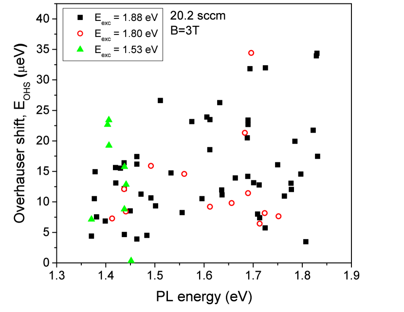
Measurements of the Overhauser shifts were repeated at T on a set of individual InAsP quantum dots emitting in a wide range of energies 1.3 - 1.8 eV as shown in Fig. 8. Circularly polarized excitation at different photon energy was employed. Excitation at =1.88 eV (squares) is in resonance with the low-energy tail of the GaInP barrier, and was previously used to induced DNP in InP/GaInP QDs Skiba-Szymanska et al. (2008); Chekhovich et al. (2011a). In addition we used =1.80 eV (circles) and =1.53 eV (triangles) to study DNP in QDs emitting at lower energies. DNP with comparable Overhauser shifts is observed for all used here. Overall, larger is observed for InAsP dots with larger emission energy that are more reminiscent of InP dots. Nevertheless, the largest eV observed here for InAsP dots is significantly smaller than in InP dots, where exceeding 120 eV has been achieved Chekhovich et al. (2010b). Since P and As have similar nuclear magnetic moments, such reduction of implies smaller degree of the optically induced nuclear spin polarization in InAsP dots. On the other hand, such reduction in DNP efficiency agrees with our hypothesis about the type-II nature of the studied dots: longer exciton lifetimes can create a bottleneck and lower the efficiency of the cyclic nuclear spin polarization process Chekhovich et al. (2010b, 2013); Urbaszek et al. (2013). Despite the smaller values, observation of pronounced DNP opens the way for future studies using optically detected nuclear magnetic resonance (NMR) spectroscopy Chekhovich et al. (2012, 2015); Checkhovich et al. (2013); Munsch et al. (2014); Waeber et al. (2016), which can provide further insights into chemical composition and strain profiles in the studied InAsP/GaInP quantum dots.
IV Conclusions
We have presented a detailed study of individual InAsP/GaInP quantum dots in samples with different arsenic content grown by MOVPE. Our samples show QD emission in a broad optical spectral range (1.3 eV to 1.8 eV), confirming successful incorporation of arsenic into the dots. The combined analysis of electron microscopy imaging, exciton diamagnetic shifts and carrier -factors measurements suggests that InAsP/GaInP dots exhibit type-II carrier confinement, where holes are localized in the InAs-rich core, while electrons reside in the InP-rich cap region. These properties make InAsP quantum dots of interest for efficient solar cell applications. Future work will include direct investigation of the type-II confinement by probing electron-hole recombination dynamics as well as further structural studies assisted by optically detected nuclear magnetic resonance techniques.
Acknowledgments
This work has been supported by the EPSRC Programme Grant EP/J007544/1. O. Del Pozo-Zamudio and J. Puebla gratefully acknowledge the support from CONACYT-Mexico Doctoral Scholarship programme. E. A. Chekhovich was supported by a University of Sheffield Vice-Chancellor’s Fellowship and a Royal Society University Research Fellowship.
References
- Bimberg and Pohl (2011) D. Bimberg and U. W. Pohl, Materials Today 14, 388 (2011).
- Sugawara (1999) M. Sugawara, ed., Self-Assembled InGaAs/GaAs Quantum Dots, Semiconductors and Semimetals, Vol. 60 (Academic Press, San Diego, 1999).
- Bimberg and Kirstaedter (1997) D. Bimberg and N. Kirstaedter, Selected Topics in Quantum Electronics, IEEE 3, 196 (1997).
- Shumway et al. (2001) J. Shumway, A. J. Williamson, A. Zunger, A. Passaseo, M. DeGiorgi, R. Cingolani, M. Catalano, and P. Crozier, Phys. Rev. B 64, 125302 (2001).
- Vinokurov and Kapitonov (1998) D. Vinokurov and V. Kapitonov, J. Exp. and Theor. Phys. Lett. 24, 623 (1998).
- Fuchi et al. (2008) S. Fuchi, S. Miyake, S. Kawamura, W. Lee, T. Ujihara, and Y. Takeda, Journal of Crystal Growth 310, 2239 (2008).
- Ribeiro and Maltez (2002) E. Ribeiro and R. Maltez, Appl. Phys. Lett. 81, 2953 (2002).
- Maltez and Ribeiro (2003) R. Maltez and E. Ribeiro, Journal of Applied Physics 94, 3051 (2003).
- Karomi et al. (2015) I. Karomi, P. M. Smowton, S. Shutts, A. B. Krysa, and R. Beanland, Opt. Express 23, 27282 (2015).
- Krysa et al. (2016) A. Krysa, J. Roberts, J. Devenson, R. Beanland, I. Karomi, S. Shutts, and P. Smowton, Journal of Physics: Conference Series 740, 012008 (2016).
- Dalacu et al. (2012) D. Dalacu, K. Mnaymneh, J. Lapointe, X. Wu, P. J. Poole, G. Bulgarini, V. Zwiller, and M. E. Reimer, Nano letters 12, 5919 (2012).
- Kosaka and Kiselev (2001) H. Kosaka and A. Kiselev, Electronics Letters 37, 464 (2001).
- van Bree et al. (2012) J. van Bree, A. Y. Silov, P. M. Koenraad, M. E. Flatté, and C. E. Pryor, Phys. Rev. B 85, 165323 (2012).
- Witek et al. (2011) B. J. Witek, R. W. Heeres, U. Perinetti, E. P. A. M. Bakkers, L. P. Kouwenhoven, and V. Zwiller, Phys. Rev. B 84, 195305 (2011).
- Kim et al. (2003) S. Kim, B. Fisher, H.-J. Eisler, and M. Bawendi, Journal of the American Chemical Society 125, 11466 (2003).
- Laghumavarapu et al. (2007) R. B. Laghumavarapu, A. Moscho, A. Khoshakhlagh, M. El-Emawy, L. F. Lester, and D. L. Huffaker, Applied Physics Letters 90, 173125 (2007).
- Ning et al. (2011) Z. Ning, H. Tian, C. Yuan, Y. Fu, H. Qin, L. Sun, and H. Ågren, Chemical Communications 47, 1536 (2011).
- Tayagaki and Sugaya (2016) T. Tayagaki and T. Sugaya, Applied Physics Letters 108, 153901 (2016).
- Dawson and Duggan (1993) M. D. Dawson and G. Duggan, Phys. Rev. B 47, 12598 (1993).
- Elliott et al. (2010) C. J. Elliott, E. A. Chekhovich, M. S. Skolnick, A. I. Tartakovskii, and A. B. Krysa, Journal of Physics: Conference Series 245, 012093 (2010).
- Bayer et al. (2002) M. Bayer, G. Ortner, O. Stern, A. Kuther, A. Gorbunov, A. Forchel, P. Hawrylak, S. Fafard, K. Hinzer, T. Reinecke, et al., Physical Review B 65, 195315 (2002).
- Chekhovich et al. (2010a) E. A. Chekhovich, M. N. Makhonin, J. Skiba-Szymanska, A. B. Krysa, V. D. Kulakovskii, M. S. Skolnick, and A. I. Tartakovskii, Phys. Rev. B 81, 245308 (2010a).
- Gotschy et al. (1989) B. Gotschy, G. Denninger, H. Obloh, W. Wilkening, and J. Schnieder, Solid State Communications 71, 629 (1989).
- Chekhovich et al. (2011a) E. A. Chekhovich, A. B. Krysa, M. S. Skolnick, and A. I. Tartakovskii, Phys. Rev. B 83, 125318 (2011a).
- Walck and Reinecke (1998) S. N. Walck and T. L. Reinecke, Phys. Rev. B 57, 9088 (1998).
- Roth et al. (1959) L. M. Roth, B. Lax, and S. Zwerdling, Phys. Rev. 114, 90 (1959).
- Sirenko et al. (1997) A. A. Sirenko, T. Ruf, M. Cardona, D. R. Yakovlev, W. Ossau, A. Waag, and G. Landwehr, Phys. Rev. B 56, 2114 (1997).
- Yugova et al. (2007) I. A. Yugova, A. Greilich, D. R. Yakovlev, A. A. Kiselev, M. Bayer, V. V. Petrov, Y. K. Dolgikh, D. Reuter, and A. D. Wieck, Phys. Rev. B 75, 245302 (2007).
- Syperek et al. (2012) M. Syperek, D. R. Yakovlev, I. A. Yugova, J. Misiewicz, M. Jetter, M. Schulz, P. Michler, and M. Bayer, Phys. Rev. B 86, 125320 (2012).
- Bastard (1991) G. Bastard, ed., Wave mechanics applied to semiconductor heterostructures (Wiley, New York, 1991).
- Peter Y. Yu (2005) M. C. Peter Y. Yu, ed., Fundamentals of Semiconductors (Springer, 2005).
- Lawaetz (1971) P. Lawaetz, Phys. Rev. B 4, 3460 (1971).
- Vurgaftman et al. (2001) I. Vurgaftman, J. R. Meyer, and L. R. Ram-Mohan, Journal of Applied Physics 89, 5815 (2001).
- Grundmann et al. (1995) M. Grundmann, O. Stier, and D. Bimberg, Phys. Rev. B 52, 11969 (1995).
- Chekhovich et al. (2013) E. A. Chekhovich, M. N. Makhonin, A. I. Tartakovskii, A. Yacoby, H. Bluhm, K. C. Nowack, and L. M. K. Vandersypen, Nature Materials 12, 494 (2013).
- Urbaszek et al. (2013) B. Urbaszek, X. Marie, T. Amand, O. Krebs, P. Voisin, P. Maletinsky, A. Högele, and A. Imamoglu, Reviews of Modern Physics 85, 79 (2013).
- Abragam (1961) A. Abragam, The Principles of Nuclear Magnetism (Oxford University Press, London, 1961).
- Gammon et al. (2001) D. Gammon, A. L. Efros, T. A. Kennedy, M. Rosen, D. S. Katzer, D. Park, S. W. Brown, V. L. Korenev, and I. A. Merkulov, Phys. Rev. Lett. 86, 5176 (2001).
- Eble et al. (2006) B. Eble, O. Krebs, A. Lemaitre, K. Kowalik, A. Kudelski, P. Voisin, B. Urbaszek, X. Marie, and T. Amand, Phys. Rev. B 74, 081306 (2006).
- Puebla et al. (2013) J. Puebla, E. A. Chekhovich, M. Hopkinson, P. Senellart, A. Lemaître, M. S. Skolnick, and A. I. Tartakovskii, Phys. Rev. B 88, 045306 (2013).
- Skiba-Szymanska et al. (2008) J. Skiba-Szymanska, E. A. Chekhovich, A. E. Nikolaenko, A. I. Tartakovskii, M. N. Makhonin, I. Drouzas, M. S. Skolnick, and A. B. Krysa, Phys. Rev. B 77, 165338 (2008).
- Chekhovich et al. (2010b) E. A. Chekhovich, M. N. Makhonin, K. V. Kavokin, A. B. Krysa, M. S. Skolnick, and A. I. Tartakovskii, Phys. Rev. Lett. 104, 066804 (2010b).
- Chekhovich et al. (2011b) E. A. Chekhovich, A. B. Krysa, M. S. Skolnick, and A. I. Tartakovskii, Phys. Rev. Lett. 106, 027402 (2011b).
- Fallahi et al. (2010) P. Fallahi, S. T. Yılmaz, and A. Imamoğlu, Phys. Rev. Lett. 105, 257402 (2010).
- Chekhovich et al. (2012) E. A. Chekhovich, K. V. Kavokin, J. Puebla, A. B. Krysa, M. Hopkinson, A. D. Andreev, A. M. Sanchez, R. Beanland, M. S. Skolnick, and A. I. Tartakovskii, Nature Nanonotechnology 7, 646 (2012).
- Chekhovich et al. (2015) E. A. Chekhovich, M. Hopkinson, M. S. Skolnick, and A. I. Tartakovskii, Nature Communications 6, 6348 (2015).
- Checkhovich et al. (2013) E. A. Checkhovich, M. M. Glazov, A. B. Krysa, M. Hopkinson, P. Senellart, A. Lemaître, M. S. Skolnick, and A. I. Tartakovskii, Nature Physics 9, 74 (2013).
- Munsch et al. (2014) M. Munsch, G. Wust, A. V. Kuhlmann, F. Xue, A. Ludwig, D. Reuter, A. D. Wieck, M. Poggio, and R. J. Warburton, Nature Nanotechnology 9, 671 (2014).
- Waeber et al. (2016) A. M. Waeber, M. Hopkinson, I. Farrer, D. A. Ritchie, J. Nilsson, R. M. Stevenson, A. J. Bennett, A. J. Shields, G. Burkard, A. I. Tartakovskii, M. S. Skolnick, and E. A. Chekhovich, Nature Physics 12, 688 (2016).