Hardware emulation of stochastic p-bits for invertible logic
Abstract
The common feature of nearly all logic and memory devices is that they make use of stable units to represent 0’s and 1’s. A completely different paradigm is based on three-terminal stochastic units which could be called “p-bits”, where the output is a random telegraphic signal continuously fluctuating between 0 and 1 with a tunable mean. p-bits can be interconnected to receive weighted contributions from others in a network, and these weighted contributions can be chosen to not only solve problems of optimization and inference but also to implement precise Boolean functions in an inverted mode. This inverted operation of Boolean gates is particularly striking: They provide inputs consistent to a given output along with unique outputs to a given set of inputs. The existing demonstrations of accurate invertible logic are intriguing, but will these striking properties observed in computer simulations carry over to hardware implementations? This paper uses individual micro controllers to emulate p-bits, and we present results for a 4-bit ripple carry adder with 48 p-bits and a 4-bit multiplier with 46 p-bits working in inverted mode as a factorizer. Our results constitute a first step towards implementing p-bits with nano devices, like stochastic Magnetic Tunnel Junctions.
Introduction
Contemporary logic and memory devices are largely built from standard MOS (metal-oxide-semiconductor) transistors, but the possibility of alternative devices based on new materials and phenomena for both Boolean and non-Boolean computation has been discussed extensively (see for example ref.Nikonov and Young (2015)). The common feature of nearly all such devices is that they make use of stable and deterministic units to represent 0’s and 1’s. A completely different paradigm is based on three-terminal stochastic units where the output is a random telegraphic signal that continuously fluctuates between 0 and 1 and the mean value can be tuned with an analog signal at the input terminal. In mathematical terms
| (1) |
where rand(1,+1) represents a random number uniformly distributed between 1 and +1, while the retention time of the p-bit is assumed large enough that memory of the last state has been lost. If the input is zero, the output takes on a value of 1 or +1 with equal probability. A negative input makes negative values more likely while a positive input makes positive values more likely.
Each such unit could be called a “p-bit” with an apparent similarity to ref.Cheemalavagu et al. (2005), and many such units can be correlated to perform useful functions by building an interconnected network where the analog input to the p-bit consists of a bias added to a weighted sum of the outputs of the other p-bits:
| (2) |
We have recently shown that with a proper choice of the matrices and , p-bit networks could be not only used to solve problems of optimization and inference Behin-Aein et al. (2016); Sutton et al. (2017) but also to implement precise Boolean functions in an invertible mode Camsari et al. (2017); Faria et al. (2017).
This invertible operation of Boolean gates is a particularly striking characteristic very different from standard digital gates which provide a unique output in response to a set of inputs. This is also true of a Boolean gate implemented with p-bits, but it additionally provides all the inputs that are consistent with a given output. Even when there is no unique input, the gate fluctuates among the multiple allowed inputs.
The inverse operation is made possible by the bidirectional nature of the interconnection matrix whereby both and are generally non-zero so that any two p-bits, say “i” and “j”, influence each other, unlike standard digital logic with directed connections. A Boltzmann Machine (BM) Ackley et al. (1985) with fully bidirectional connections, (all ) , would put inputs and outputs on an equal footing. However, a BM would normally provide approximate answers without the kind of accuracy expected from digital logic. A directed network of bidirectional BM’s, on the other hand, has been shown to provide a striking combination of digital accuracy and logical invertibility.
These demonstrations of accurate invertible logic are intriguing, but they are based on purely software implementations of Eqs. (1,2) and it is natural to ask whether real hardware implementations of these equations would preserve these striking properties. It is well-established that software implementations of unrestricted Boltzmann Machines need to be serially updated to ensure proper operation and convergenceSuzuki et al. (2013); Hinton (2007). In software, this is enabled by control flow statements such as“for-loops” that make each update one by one, negatively impacting performance. How does this carry over to hardware implementations? In our hardware emulation, the serial updating of p-bits comes naturally without any peripheral control circuity. This is due to the asynchronous operation of p-bits that result from natural time delays between p-bits. In simulation p-bits are assumed identical, but how will inevitable process variations in real p-bit retention time effect the system operation? This paper represents a first step in answering these questions using individual microcontrollers to emulate p-bits described by Eq. (1), while the interconnections described by Eq. (2) are implemented by another microcontroller.
Our approach is quite similar to ref. 10, where electronic versions of synapses and neurons are built using off-the-shelf technology to demonstrate experimentally the formation of associative memory in a simple neural network consisting of three electronic neurons connected by two memristor-emulator synapses. Clearly our microcontroller based emulation of p-bit networks is not very scalable. But we envision that the interconnect between stochastic p-bits can be efficiently built using contemporary CMOS solutions and that nanodevices would be needed to build more efficient stochastic p-bits. This work primarily motivates such an endeavor and we develop essential rules of operation for such future systems.
While the long term goal is to develop miniature integratable devices, the hardware emulation presented here has many of its important features. The variables and appearing in Eqs. (1) and (2) are not symbols represented in software, but actual voltages that can be observed and measured with oscilloscopes and voltmeters. The variability in the operation of real p-bits can be included by programming each microcontroller to have a different retention time, . Interconnect delays can be included into Eq. (2) as desired. The hardware implementation also allows us to establish important hardware rules for “interconnect delays” and retention times of p-bits, by systematically varying these time-constants.
Note that hardware implementations of Boltzmann Machines exist where Eq.(2) is implemented in dedicated hardware while Eq. (1) has been simulated off chip. Both Eqs. (1,2)have have been used as basis for dedicated VLSI based hardware implementations that perform various combinatorial optimization problems Yoshimura et al. (2016); Okuyama et al. (2016) as well as hybrid architectures in context of learning Kim et al. (2009); Ly and Chow (2009); Jarollahi et al. (2014); Hu et al. (2015); Ardakani et al. (2017); Wang et al. (2017) and combinatorial optimization Bojnordi and Ipek (2016). This work, however, is focused on invertible Boolean logic, and is configured in a way that should be isomorphic with actual hardware implementations, where each microcontroller emulating a p-bit could be replaced with a specific hardware unit, such as a stochastic magnetic tunnel junction Locatelli et al. (2014); Piotrowski et al. (2016); Grollier et al. (2016), as we progress.
To distinguish our PSL from other probabilistic logic concepts, it is necessary to put things into a historical context. The term “stochastic computing” or “probabilistic computing” has been used since 1960’s. The pioneering work of von Neumann Von Neumann (1956), Gaines Gaines et al. (1969) and Poppelbaum et al. Poppelbaum et al. (1967) addressed the reliable implementation of Boolean algebra and probabilistic arithmetic using stochastic components and established a field called “stochastic computing”. The major attraction of stochastic computing lies in its low complexity arithmetic units and inherent error tolerance.
A basic feature of stochastic computing is that numbers are represented by streams of bits that can be processed by simple circuits like AND gates, while the outputs are statistically counted as probabilities under both normal and faulty conditions. However, despite the advantages mentioned above, stochastic computing has been considered impractical because it takes a large number of bits to represent a value and does not show a cost advantage in multiplication – a prototypical inexpensive stochastic operation, when precision and reliability are required. Also the building block of such a system Onizawa et al. (2016) will resemble some proposals Camsari et al. (2017) of p-bits for PSL, but as we will describe in the next section, they are fundamentally different in their requirement to simultaneously read and write. An increase in the precision of a stochastic computation requires an exponential increase in bit-stream length, implying an exponentially increased computation time Alaghi and Hayes (2013) Manohar (2015), which is undesirable. To be clear: We are not following this type of probabilistic approach but instead use a probabilistic architecture that offers substantial advantages over conventional computational schemes as described above.
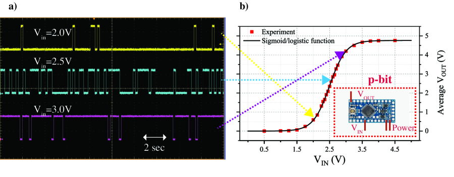
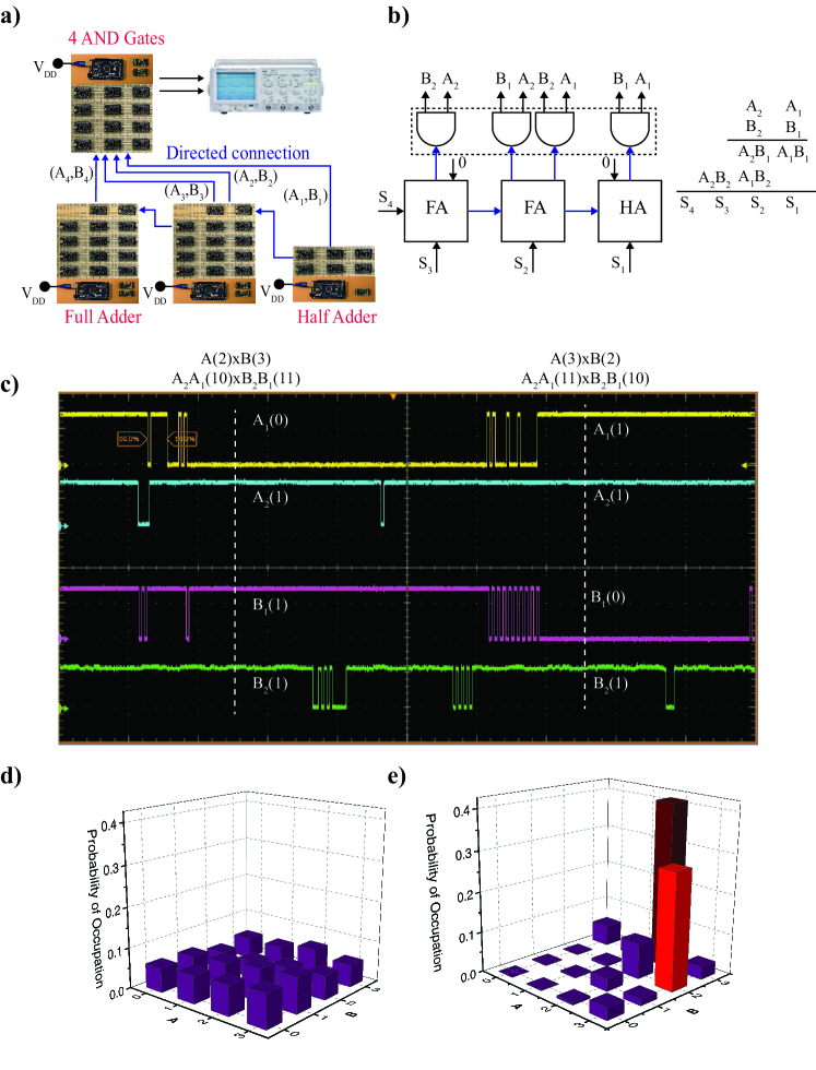
Next we describe the approach we are using to perform a hardware emulation of Eqs. (1) and (2). Fig. 1 shows an emulation of a p-bit using a microcontroller. We then present a 3 p-bit Boltzmann Machine implementing an AND gate in both direct and inverted modes of operation (Figs. 2,3) and evaluate the role of sampling and retention times in ensuring proper operation (Figs. 4,5,6). We then present results for binary adders in both direct and inverted modes (Figs. 7,8), and end with results for a 4-bit multiplier working in the inverted mode as a factorizer (Fig. 9).
Methods
Arduino pro mini as a p-bit
A version of Eq. (1) suitable for microcontroller based emulation of a p-bit is given as
| (3) |
where and are the digital output and analog input voltages of the p-bit and S(x) is a sigmoidal function given by,
| (4) |
I/O characteristics: An Arduino pro mini is a 24 pin microcontroller ard that can be programmed to emulate the behavior of Eq. (3) as shown in Algorithm 1. It has 6 dedicated analog input pins that have very high input resistances (100 M) along with 6 dedicated PWM (Pulse-width modulation) output pins that have very low output resistances (100 ) with the ability to source 40 mA of current. This allows the Arduino to behave as a voltage controlled voltage source.
p-bit operation: The time evolution of the output voltage for a set of input voltages using an oscilloscope (Tektronix DPO7104) is shown in Fig. 1(a). As the input voltage is varied from low to high, the microcontroller generates more 1’s than 0’s. DC average measurements of the output voltage taken over 100 seconds are also shown in Fig. 1(b). The average voltage follows the sigmoidal function which indicates the tunable nature of the p-bit.
Retention time : Each p-bit is characterized by a retention time () for which the output voltage is held constant. A possible physical component in the implementation of p-bits is the superparamagnet Camsari et al. (2017):
| (5) |
where is a material dependent quantity ranging from 1 ps to 1 ns Lopez-Diaz et al. (2002), is the energy barrier of the nanomagnet and is the Boltzmann energy. For superparamagnets that are in the 1020 range, the characteristic time is in the ms regime, assuming a of 1 ns. We emulate the retention time in our p-bits using a user defined delay as shown in Algorithm 1. We later study the effect of retention time and establish some essential rules for proper operation of our interconnected p-bits.
Weight Logic using microcontroller and DAC
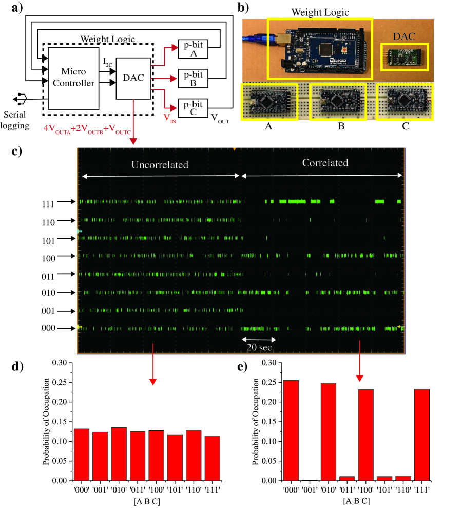
Fig. 2(a,b) shows a schematic and a block diagram for a 3 p-bit Boltzmann Machine that is programmed as an AND gate. The electrical wires connecting the components are not shown for clarity. The p-bits are correlated using a weight logic block that computes the input voltage of the p-bit using the output voltages of all other p-bits in the network using
| (6) |
where is the time interval for which the input voltages are held constant. Eq. (6) is a modified version of Eq. (2), meant to be used for our voltage controlled voltage source p-bits.
Arduino mega as weight logic: Our weight logic is implemented using an Arduino mega microcontroller in conjunction with MAXIM 5825 Digital to Analog converters max . The Arduino mega can read as many as 52 digital inputs and communicates with the DAC using a fast protocol. The DAC has 8 channels with each having a 10-bit resolution. A pseudocode for programming an Arduino mega to emulate Eq. (6) is given in Algorithm 2. The input voltages of the p-bits set by Eq. (6) are not constrained in general, however we limit them to the p-bit input range between 0 and 5 Volts. Note that the weight logic not only correlates the p-bits, but can also be used for monitoring and recording the state of the Boltzmann Machines. Fig. 2(c,d,e) show two possible methods for monitoring the state of the system which are,
-
•
Artificial nodes set through the DAC: The microcontroller and the DAC can be used to create artificial voltage nodes that can be used to concurrently read the output of the p-bits as a single voltage. For example, in the operation of the AND gate (), 4A+2B+C is evaluated and set as a voltage in Fig. 2(c) to monitor the state of the AND gate.
-
•
Serial logging: The microcontroller that is part of the weight logic can also be used to log data through a serial port connection (USB). We have used this method extensively for collecting steady-state (long time) statistics for the various Boltzmann Machines that we present in this paper.
Note that even though artificial nodes can be used to monitor the correlations of p-bits, serial logging of the data is much more convenient to collect long time statistics.
Communication between the DAC and Arduino mega: The DACs use the protocol that allows the Arduino mega microcontroller to communicate with two pins SDA(Data) and SCL(Clock). When the system is first turned on, the DACs need to be initialized. This requires knowing the addresses of the individual DACs that are connected and setting a reference voltage for the DAC. We utilize at most 2 DACs within a Boltzmann Machine and the addresses for those are adjusted using two jumpers on the DAC. For example, to write a voltage of 2.5 V to channel 4 of the DAC whose address is set at “0x20”, we could send the following 4 bytes over the interface: byte1 [0010000], byte2 [10110011], byte3 [10000000], byte4 [00000000]. The first byte has the address of the DAC in its 4 LSBs. The 4 MSBs of byte 2 has a command signal of writing to whichever channel is specified by the 4 LSBs of byte 2. The first 10 bits of byte 3 and 4 are the decimal equivalent of 512 which constitutes 2.5 V for a 10 bit DAC with 5V reference voltage. A library was written to internalize these operations, allowing the user to simply set voltages using a single write command that only uses the channel number and voltage for operation.
Results
AND Gate as a Boltzmann Machine
Correlated network of p-bits: Fig. 2(c) shows the output voltage of an artificial node (4A+2B+C) as a function of time on the oscilloscope. For the AND gate the and are taken from Biamonte (2008). The strength of correlation between p-bits is adjusted through the parameter in Eq. (2). can be thought as the inverse (pseudo) temperature, in the sense that as increases the p-bits get strongly correlated. When the system is uncorrelated by using a , the 3 p-bits are independent of each other, resulting in the artificial node being uniformly distributed between 0 and 7, which can be seen from the steady state statistics for as shown in Fig. 2(d). However, when the system is correlated using an , it locks to the states prescribed by and matrices, corresponding to the lines of the truth table for an AND gate which is shown by the steady-state statistics for in Fig. 2(e). Note that we have left all the inputs and outputs floating, which results in all the lines of the truth table getting highlighted as is increased. This “floating” mode of operation is a unique feature of correlated p-bits. The statistics shown in Fig. 2(d,e) have been collected through serial logging through the weight logic for up to half a million samples.
Clamping p-bits: For Boolean computation, the p-bits need to be clamped to produce a given output. This is done by simply connecting the input voltage of the p-bit to either ground or 5 V. This in essence corresponds to applying a large bias, , to a given p-bit according to Eq. (6). A clamped p-bit operates on the corners of the sigmoidal response shown in Fig. 1(b). Note that the input and output bits of a Boltzmann Machine are on an equal footing and can be clamped for direct and inverted operation respectively, as we discuss below.
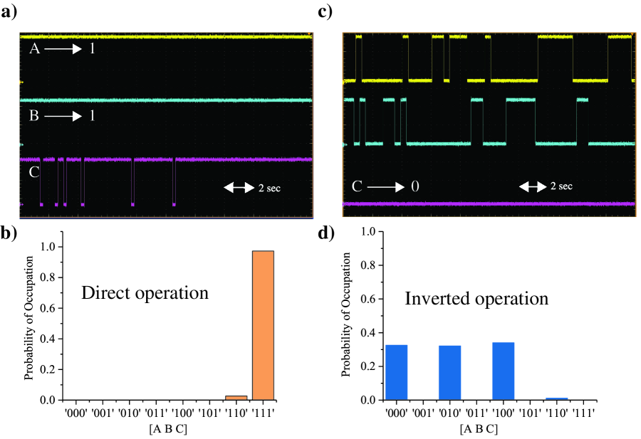
Direct Operation: Fig. 3 shows two cases of using an AND gate for computation purposes. Fig. 3(a) shows the time evolution of output voltages of p-bits A and B being clamped to 1 on the oscilloscope. As a result, the output voltages of C mostly stay in 1 as shown. This is also confirmed by the steady state statistics shown in Fig. 3(b) which are acquired using serial logging through the weight logic.
Inverted Operation: A remarkable feature of the design is the inverted operation. Fig. 3(c) shows the time evolution of output voltages for A, B and C when C is clamped to 0. It can be seen that A and B follow the states prescribed by lines of the truth table of an AND gate, as shown in Fig. 3(d). This feature stems from the fact that the system places all p-bits, whether input or output, on an equal footing. It is this inverted operation that can be used to solve more complex problems such as the 4-bit factorizer presented later in this paper.
Sampling and retention time
Consider the Boltzmann Machine presented in Fig. 2. For each such network there are two major time constants:
-
•
Retention time : Time interval for which the output voltage is held constant by the p-bit.
-
•
Sampling time : The time interval for which the input voltages to the p-bits are held constant by the weight logic. The sampling time can be thought of as the sum of the user defined delay of Algorithm 2 and the time it takes to compute everything else in the Repeat block of Algorithm 2.
Boltzmann Law: We now study the effect of both these time constants on the operation of the system using the AND gate. For such networks of correlated p-bits, an energy functional E for the state can be defined as Camsari et al. (2017):
| (7) |
The Boltzmann Law accurately captures the steady state probabilities of the system to be in different states according to,
| (8) |
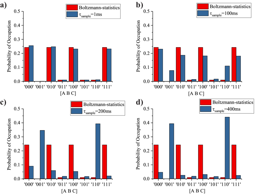
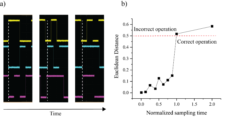
Sampling time distribution: Fig. 4 shows the steady state statistics of an AND gate with each of the three p-bits having , with their sampling times varying from 1 ms to 400 ms. It can be seen from Fig. 4(a) that for extremely small the behavior of the system is captured well by the Boltzmann law. However as is increased to 100 ms, two incorrect states 001 and 110 stand out more. As is increased to 200 ms, the system breaks down completely, with only the 001 and 110 states being highlighted. This continues for all greater then 200 ms as shown by .
We observe that when the sampling time is close to the retention time (), Fig.5(b) shows the euclidean distance between steady state distributions for various normalized sampling times ( sampling times from 1 ms to 400 ms with p-bit retention time of 200 ms). We observe that a boundary () exists for proper operation of the system. Around this boundary, p-bits can change their state before their input to the other p-bits are communicated, and this results in an incorrect operation. However, for fast sampling , the updating is approximately instantaneous. It is important to note that this requirement of necessitates a fast weight logic operation in any hardware implementation of p-bits.
An essential requirement for Hopfield networks and unrestricted Boltzmann Machines is the need for sequential updating, where each p-bit is updated serially but in any random order Amit (1992); Suzuki et al. (2013), as opposed to parallel updating where each p-bit is updated at once. To enforce serial updating in asynchronous networks in simulation requires control flow statements which regulate the updating procedure of p-bits to one by one. Serial updating arises naturally in our setup since each p-bit is completely independent of each other and small phase differences that are present initially get greatly magnified as the system is run for longer periods of time, in the absence of a central clock signal. This type of updating is also known as the “asynchronous dynamic” in Hopfield networks Amit (1992). This is shown for an AND gate with 3 p-bits in Fig.5(a), where each of the 3 p-bits are almost perfectly aligned to each other initially, however this alignment is broken as system continues to run with time. Asynchronous machines are known to converge slowly, while their synchronous counterparts allow for parallel updating, allowing much faster convergence. For hardware implementations, it is the synchronous Boltzmann Machines or Restricted Boltzmann Machines that would require some master control to ensure parallel updating making the system grow in resources as the number of p-bits increase.
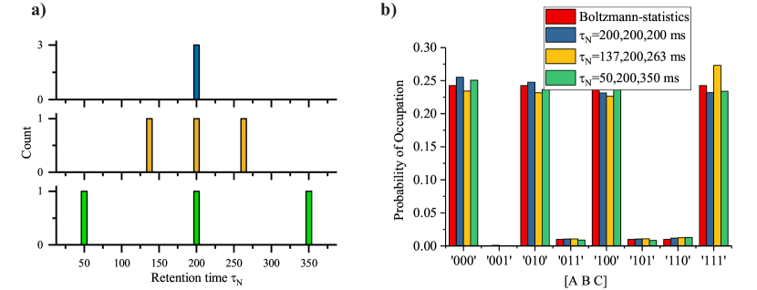
Retention time distribution: We now investigate the behavior of an AND gate in the presence of p-bits with different retention times that would arise due to inevitable process variations in a nanoscale implementation. Fig. 6(a) shows the histogram for three different retention time configurations of the AND gate. In the most trivial case, all three p-bits have the same retention time while having a sampling time . The steady state statistics for this case exhibit a good match with the Boltzmann law (Fig. 6(b)). However, this configuration is unlikely in the case of any physical system where some distribution is to be expected due to process variations.
A more realistic scenario is that of the 3 p-bits having different retention times. Fig. 6(a) shows two cases where p-bits are distributed in two sets of {137, 200, 263} ms and {50, 200, 350} ms with a spread of and around the mean value of 200 ms respectively, while maintaining very fast sampling times of . Both cases show a good match with the Boltzmann Law (Fig. 6(b)). We conclude that if the sampling time is much greater than the smallest , the system operation is well described by the Boltzmann Law, which can be attributed to the much reduced probability of parallel updating.
Full Adder as a Boltzmann Machine
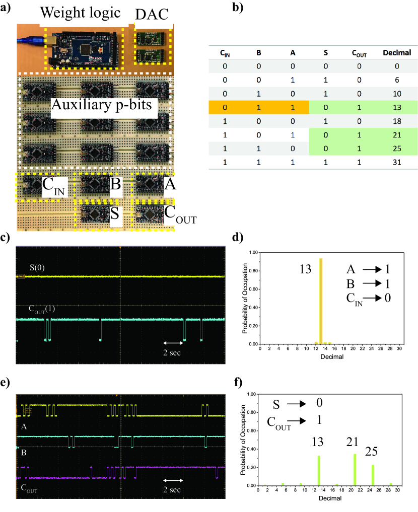
Fig. 7(a) shows a schematic of a 14 p-bit Full Adder implemented as a Boltzmann Machine. Of the 14 p-bits only 5 serve as the actual terminals of the Full Adder while the remaining 9 are auxiliary p-bits. The retention and sampling times are chosen as for all the p-bits with a . However, now two DACs are needed to set the input voltages for all the p-bits since each DAC has 8-channels.
The design of [J] and matrices follows the treatment presented in Camsari et al. (2017). Direct computations can be performed by clamping p-bits as discussed earlier. Fig. 7(c,d) shows an example of 1-bit binary addition.The inputs A, B and have been clamped to 110 respectively, and the time evolution of output the voltages of S and are shown in Fig. 7(c) which follow the states prescribed by the truth table of the Full Adder. This can also be seen from the steady state statistics shown in Fig. 7(d) which have been collected through serial logging.
Similar to the AND gate, the Full Adder implemented as a Boltzmann Machine can also be operated in inverted mode. The time evolution of the the inputs A, B and are shown in Fig. 6(e) when the outputs S and are clamped to 0 and 1 respectively. The inputs A, B and follow the three prescribed states of the Full Adder truth table which is also confirmed by the steady state statistics shown in Fig. 7(f).
Directed Networks of Boltzmann Machines
To build more complex systems, one possible approach is to design the entire system as a single Boltzmann Machine, but the reversible nature of the Boltzmann Machines can hinder in the correct operation of such systems Camsari et al. (2017). A more practical alternative is to interconnect simpler Boltzmann Machines with directed connections to build up more complex systems such as a 4-bit Ripple Carry Adder (RCA) (Fig.8(a)) or a 4-bit multiplier/factorizer (Fig.9(a)).
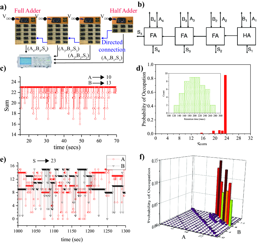
Directed Connections: Separate Boltzmann Machines can be connected in a directed fashion such that the connections between the two are not reciprocal . In hardware, this corresponds to disconnecting the input voltage of p-bit “i” from its native weight logic and connecting to it the output voltage of p-bit “j” from a different Boltzmann Machine so that . Consider the case of a 4-bit adder that is built using a Half Adder and 3 Full Adders. In this case there are 3 directed connections as shown in Fig. 8(a). Each connection takes the output voltage of of the adder and connects it to the input terminal of of the adder. Due to this connection scheme, no information can flow from the adder to the adder, which makes the system no longer bidirectional. However, as noted in Camsari et al. (2017), bidirectional connections of adders hinders proper operation of a n-bit adder. Also note that since the connection from one Boltzmann Machine to another is an electrical connection, the strength of the correlation between the two machines is at most 1 ().
4-bit Adder: We next demonstrate the correct operation of a 4-bit RCA comprised of 48 p-bits each having different as shown in the inset of Fig. 8(d). The values of are normally distributed around an average of 200 ms with a minimum of 137 ms to a maximum of 263 ms, with a sampling time of 10ms for all Full Adders. 4-bit binary addition is performed by clamping the input p-bits of each adder, as demonstrated by the time evolution of the sum shown in Fig. 8(c) with A=10 and B=13 resulting in the sum being 23 when converted to decimal. We observed for AND gates that their exists a boundary for proper operation of Boltzmann Machines with all p-bits having the same retention time. Similarly with a distribution such as the one studied here there also exists a boundary for proper operation which is . This is due to the interconnect delays that need to be small.
Inverted mode: A more remarkable case is that of the sum bits of each of the adders being clamped to S=23, with A and B left floating. In this case, A and B fluctuate among 8 possible integer combinations that satisfy A+B=23. Note that since A and B are 4-digit binary numbers, not all integer combinations can be probed by the system, for example A=22 and B=1. This can be seen from the histogram presented in Fig. 8(f). Although there are 8 peaks in the histogram, the height of each peak is not the same since statistics presented in Fig. 8(f) are not exactly steady state. With 48 p-bits in the system, the number of samples needed for steady state statistics is prohibitively large. Unrestricted Boltzmann Machines converge slower compared to restricted Boltzmann MachinesHinton (2007), but since asynchronous updates come naturally in hardware while synchronous updating will require more control circuitry, a design choice needs to be made between resources utilized and speed of convergence. Although it still remains to be seen how much of an improvement in the speed of convergence can be achieved by RBM’s as compared to unrestricted Boltzmann machines.
4-bit multiplier/factorizer: In this final example, we show how a standard digital multiplier built out of AND gates and Full Adders can be operated in reverse to function as a factorizer as shown in Fig. 9, similar to what was proposed in Traversa and Ventra (2017) in the different context of memcomputing. Implementation of practically useful factorizers usually requires dedicated algorithms, here our purpose is simply to illustrate the remarkable invertibility of directed networks of p-bits.
The block diagram of a digital multiplier is shown in Fig. 9(b). The individual bits of A and B are first multiplied to produce , , and which are then added together to produce the product S. To convert this multiplier to a factorizer, we reverse the directed connections from the AND gates to the adders, while keeping the original directed connections of the Full Adders from the LSB to the MSB.
The output voltages from the and (where X is the Full Adder) are now sent as inputs to the output p-bits of the 4 AND gates. The 4 AND gates used here are part of one Boltzmann Machine instead of 4 separate Boltzmann Machines. This is because some inputs of the AND gates need to be the clones of each other as they go to different gates. For example, in Fig. 9(b), is a common input for the two right most AND gates, while is a common input for the two left most AND gates. The retention and sampling times are chosen as for all the p-bits with a .
Fig. 9(c) shows the time evolution of output voltages of and using an oscilloscope when the sum of the adder is clamped to 6. This results in the input p-bits of the AND gates producing the correct factors of 32 and 23. This can also be seen by the statistics of the input p-bits of the AND gate as shown in Fig. 9(e). As previously, the heights of both peaks are not the same due to the statistics not being exactly steady state. The results are collected through serial logging via the Boltzmann Machine for the AND gates. For comparison, we also show the statistics for an uncorrelated factorizer where 16 combinations are equally probable as shown in Fig. 9(d).
References
- Nikonov and Young (2015) D. E. Nikonov and I. A. Young, IEEE Journal on Exploratory Solid-State Computational Devices and Circuits 1, 3 (2015).
- Cheemalavagu et al. (2005) S. Cheemalavagu, P. Korkmaz, K. V. Palem, B. E. Akgul, and L. N. Chakrapani, in IFIP International Conference on VLSI (2005) pp. 535–541.
- Behin-Aein et al. (2016) B. Behin-Aein, V. Diep, and S. Datta, Scientific Reports 6, 29893 (2016).
- Sutton et al. (2017) B. Sutton, K. Y. Camsari, B. Behin-Aein, and S. Datta, Scientific Reports 7, 44370 (2017).
- Camsari et al. (2017) K. Y. Camsari, R. Faria, B. M. Sutton, and S. Datta, Phys. Rev. X 7, 031014 (2017).
- Faria et al. (2017) R. Faria, K. Y. Camsari, and S. Datta, IEEE Magnetics Letters 8, 1 (2017).
- Ackley et al. (1985) D. H. Ackley, G. E. Hinton, and T. J. Sejnowski, Cognitive science 9, 147 (1985).
- Suzuki et al. (2013) H. Suzuki, J.-i. Imura, Y. Horio, and K. Aihara, Scientific reports 3, 1610 (2013).
- Hinton (2007) G. E. Hinton, Scholarpedia 2, 1668 (2007).
- Yoshimura et al. (2016) C. Yoshimura, M. Hayashi, T. Okuyama, and M. Yamaoka, in Computing and Networking (CANDAR), 2016 Fourth International Symposium on (IEEE, 2016) pp. 436–442.
- Okuyama et al. (2016) T. Okuyama, C. Yoshimura, M. Hayashi, and M. Yamaoka, in Rebooting Computing (ICRC), IEEE International Conference on (IEEE, 2016) pp. 1–8.
- Kim et al. (2009) S. K. Kim, L. C. McAfee, P. L. McMahon, and K. Olukotun, in Field Programmable Logic and Applications, 2009. FPL 2009. International Conference on (IEEE, 2009) pp. 367–372.
- Ly and Chow (2009) D. L. Ly and P. Chow, in Proceedings of the ACM/SIGDA international symposium on Field programmable gate arrays (ACM, 2009) pp. 73–82.
- Jarollahi et al. (2014) H. Jarollahi, N. Onizawa, V. Gripon, N. Sakimura, T. Sugibayashi, T. Endoh, H. Ohno, T. Hanyu, and W. J. Gross, IEEE Journal on Emerging and Selected Topics in Circuits and Systems 4, 460 (2014).
- Hu et al. (2015) S. Hu, Y. Liu, Z. Liu, T. Chen, J. Wang, Q. Yu, L. Deng, Y. Yin, and S. Hosaka, Nature communications 6 (2015).
- Ardakani et al. (2017) A. Ardakani, F. Leduc-Primeau, N. Onizawa, T. Hanyu, and W. J. Gross, IEEE Transactions on Very Large Scale Integration (VLSI) Systems (2017).
- Wang et al. (2017) C. Wang, L. Gong, Q. Yu, X. Li, Y. Xie, and X. Zhou, IEEE Transactions on Computer-Aided Design of Integrated Circuits and Systems 36, 513 (2017).
- Bojnordi and Ipek (2016) M. N. Bojnordi and E. Ipek, in High Performance Computer Architecture (HPCA), 2016 IEEE International Symposium on (IEEE, 2016) pp. 1–13.
- Locatelli et al. (2014) N. Locatelli, A. Mizrahi, A. Accioly, R. Matsumoto, A. Fukushima, H. Kubota, S. Yuasa, V. Cros, L. G. Pereira, D. Querlioz, et al., Physical Review Applied 2, 034009 (2014).
- Piotrowski et al. (2016) S. K. Piotrowski, M. Bapna, S. D. Oberdick, S. A. Majetich, M. Li, C. L. Chien, R. Ahmed, and R. H. Victora, Phys. Rev. B 94, 014404 (2016).
- Grollier et al. (2016) J. Grollier, D. Querlioz, and M. D. Stiles, Proceedings of the IEEE 104, 2024 (2016).
- Von Neumann (1956) J. Von Neumann, Automata studies 34, 43 (1956).
- Gaines et al. (1969) B. R. Gaines et al., Advances in information systems science 2, 37 (1969).
- Poppelbaum et al. (1967) W. J. Poppelbaum, C. Afuso, and J. W. Esch, in Proceedings of the November 14-16, 1967, Fall Joint Computer Conference, AFIPS ’67 (Fall) (ACM, New York, NY, USA, 1967) pp. 635–644.
- Onizawa et al. (2016) N. Onizawa, D. Katagiri, W. J. Gross, and T. Hanyu, IEEE Transactions on Nanotechnology 15, 705 (2016).
- Alaghi and Hayes (2013) A. Alaghi and J. P. Hayes, ACM Transactions on Embedded computing systems (TECS) 12, 92 (2013).
- Manohar (2015) R. Manohar, IEEE Computer Architecture Letters 14, 119 (2015).
- (28) “Arduino - www.arduino.cc,” .
- Lopez-Diaz et al. (2002) L. Lopez-Diaz, L. Torres, and E. Moro, Physical Review B 65, 224406 (2002).
- (30) “Maxim dac - www.maximintegrated.com,” .
- Biamonte (2008) J. Biamonte, Physical Review A 77, 052331 (2008).
- Amit (1992) D. J. Amit, Modeling brain function: The world of attractor neural networks (Cambridge University Press, 1992).
- Traversa and Ventra (2017) F. L. Traversa and M. D. Ventra, Chaos: An Interdisciplinary Journal of Nonlinear Science 27, 023107 (2017).
Acknowledgments
It is a pleasure to acknowledge many helpful discussions with Brian Sutton ( Purdue University). We are also grateful to Zhihong Chen (Purdue University) for discussions on stochastic computing. This work was supported in part by C-SPIN, one of six centers of STARnet, a Semiconductor Research Corporation program, sponsored by MARCO and DARPA, in part by the Nanoelectronics Research Initiative through the Institute for Nanoelectronics Discovery and Exploration (INDEX) Center, and in part by the National Science Foundation through the NCN NEEDS program, contract 1227020-EEC.
Author contributions statement
Authors ( A.Z.P and L.A.G ) participated in conducting the experiments, while all authors ( A.Z.P, L.A.G, K.Y.C and S.D) helped in analyzing the results, reviewing and writing the manuscript.
Additional information
Competing financial interests The authors declare no competing financial interests.
