Charging of highly resistive granular metal films
Abstract
We have used the Scanning Kelvin probe microscopy technique to monitor the charging process of highly resistive granular thin films. The sample is connected to two leads and is separated by an insulator layer from a gate electrode. When a gate voltage is applied, charges enter from the leads and rearrange across the sample. We find very slow processes with characteristic charging times exponentially distributed over a wide range of values, resulting in a logarithmic relaxation to equilibrium. After the gate voltage has been switched off, the system again relaxes logarithmically slowly to the new equilibrium. The results cannot be explained with diffusion models, but most of them can be understood with a hopping percolation model, in which the localization length is shorter than the typical site separation. The technique is very promising for the study of slow phenomena in highly resistive systems and will be able to estimate the conductance of these systems when direct macroscopic measurement techniques are not sensitive enough.
pacs:
64.60.ah, 71.23.An 72.20.EeI Introduction
During the last decades, slow conductance relaxation has been studied in many disordered insulators and, in particular, in granular metals by means of field effect measurements. After a quench at low temperatures, a change in the gate voltage is accompanied by a sudden increase in the conductivity, which subsequently slowly decreases with a roughly logarithmic dependence on time VaOv02 ; Grenet2007 ; Ovadyahu2007 ; HaEi12 . Memory effects and aging are often seen in the same type of experiments Grenet2010 . All these glassy effects have been interpreted in different ways, but there is a growing tendency to explain them in terms of electron glasses, i.e., systems with states localized by the disorder and long-range Coulomb interactions between carriers Pollak06 ; POF13 ; Amir15 .
These glassy effects were first limited to low temperature , but they have recently been observed at room temperature in discontinuous Au Eisenbach2016 , amorphous NbSi Delahaye2014 and granular Al films granular . In addition, high resolution techniques such as scanning force microscopy (SFM) open the possibility of studying these systems at room temperature allowing a detailed real space analysis of the problem. Some of us have applied the SFM technique to study slow relaxation in the surface potential of conducting polymers Ortuno2016 . We observed logarithmic relaxation over four decades of time, as well as full aging in terms of the time of application of the gate voltage. The technique proved appropriate to monitor slow relaxation at the nanoscale.
The use of local probe techniques, such as scanning Kelvin probe microscopy (SKPM), presents two advantages as compared with the conductance measurements performed so far: i) it allows a study of the phenomena at the nanometer scale, which can shed some light on the mesoscopic effects at work in the conductance relaxations, previously observed in indium oxide Orlyanchik and granular Al films Delahaye2008 , but not fully understood; ii) samples with larger resistances can be measured, which is interesting because we know that in the “electron glass” experiments, the larger the resistance, the larger the conductance relaxations (in % of conductance).
In this problem the first question to answer is the mechanism of charge injection in a strongly disordered insulator. It is an interesting general question and has rarely been addressed. The most thorough study on this subject was the work by Adkins’ group adkins ; adkins84 . Analysing non local electrical measurements, they found that inhomogeneities play a crucial role in the charging process and that the scale of inhomogeneities grows as the proportion of metal increases and grains coalesce. They also found strong evidence for the percolative nature of both transport and the charging process. Finally, they monitored the total charge accumulated in the sample as a function of time and observed that the corresponding time dependence was clearly broader than the predictions of diffusion models. In discontinuous metal films and in many other strongly insulating systems, the basic assumption of the conduction models is the exponential-like distribution of the microscopic hopping rates POF13 . Its implications in macroscopic transport properties have been systematically confirmed. It gives rise, for example, to the widely observed variable-range hopping TsEf02 ; SoOr06 , but no direct microscopic evidence have been produced so far.
In this paper, we study with the SFM technique the time evolution and the spatial dependence of the surface potential of granular Al thin films when a gate voltage is suddenly applied and later on switched off, after a relatively long period of time. We measure samples that are qualitatively similar to those previously studied by some of us in the context of slow relaxation in the conductivity, but that have been grown with the appropriate resistance for this experiment, that is, with a resistance high enough to ensure that the charging processes take place in the scale from milliseconds to hours. As our experimental results are difficult to understand with a model of homogeneous conductivity, we have constructed a more general network resistance-capacitance model able to handle strong inhomogeneities Ortuno:2015 .
In the next section we describe the SFM technique employed and how the samples have been grown. In section III we present the experimental results, first for the charging experiments and later for the discharging experiments. In section IV we introduce our network model and describe the results of the numerical simulations. Finally, we extract some conclusions.
II Experimental method
II.1 Sample preparation
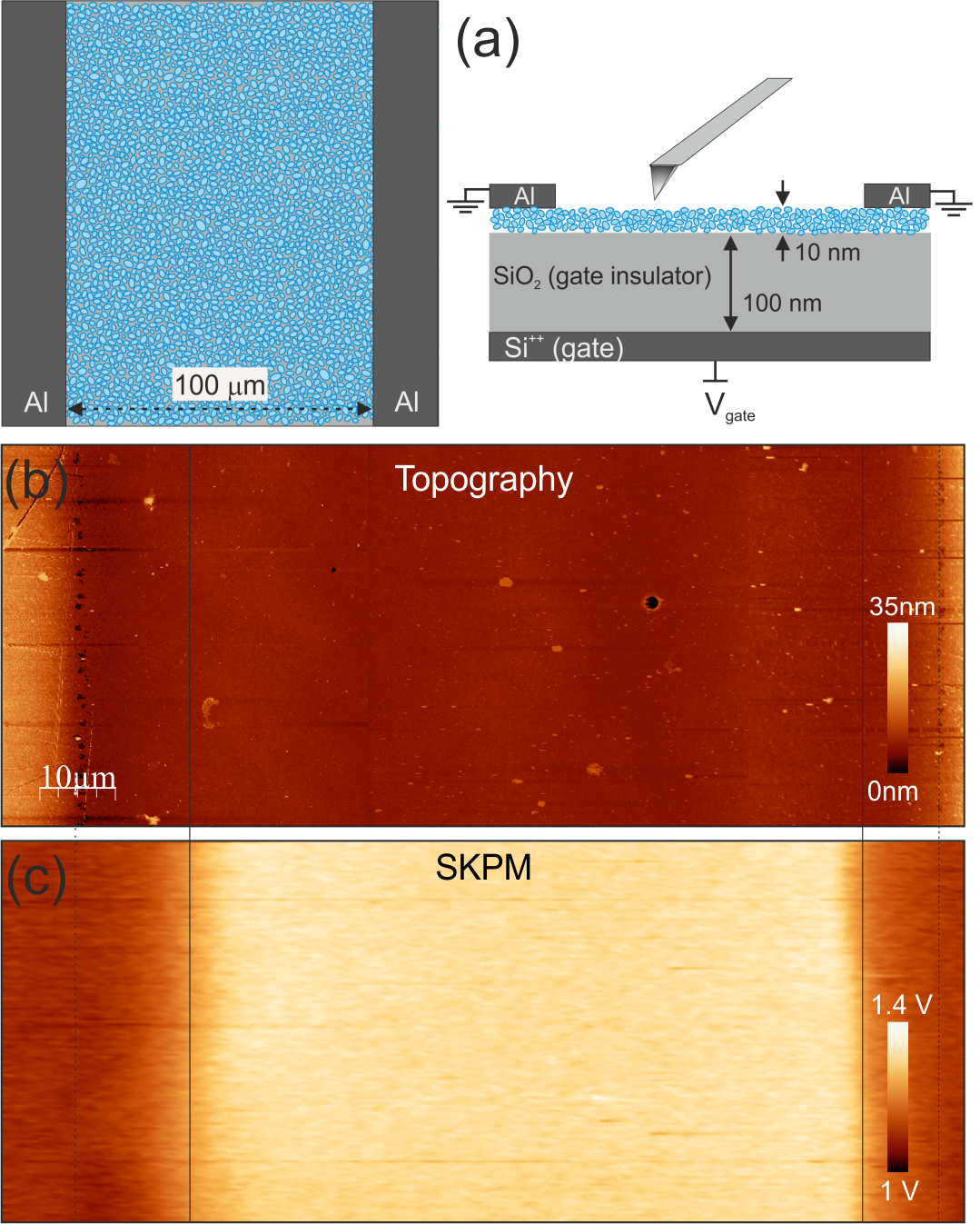
The horizontal and vertical schemes of the sample are shown in Fig. 1 (a). The granular Al films used in this study were prepared as described elsewhere by the e-beam evaporation of pure Al under a partial pressure of oxygen Grenet2007 . The parameters here are an Al evaporation rate of 1.8 A/s and a partial oxygen pressure around mbar, for a film thickness of 10 nm. Beyond an oxygen pressure of about mbar, the resistance of the films cannot be measured with our experimental set-up at room temperature (their resistance per square is larger than G). Previous X rays and TEM investigations have revealed that such films are made of crystalline Al grains of a few nanometers size, dispersed in an amorphous alumina matrix. For the SFM Kelvin probe investigations, the granular Al films were deposited on top of heavily doped Si wafers (the gate) coated with a 100 nm layer of thermally grown SiO2 (the gate insulator). Al contacts 30 nm thick and evaporated on the granular Al film without opening the e-beam evaporation chamber define channels 30-100 micrometers wide (see the topographic picture). No leaking current to the gate was detected (smaller than 1 pA).
II.2 SFM microscopy
SFM measurements were carried out using a Nanotec SFM system with a PLL/dynamic measurement board. Once the SFM tip was placed in the granular Al channel between the two lateral contacts topography and surface potential images were acquired simultaneously by means of scanning Kelvin probe microscopy (SKPM) at room temperature and ambient conditions using Pt-coated tips (OMCL- AC240TM-R3, nominal N/m). To assure quantitative measurements data were acquired in frequency modulation non-contact dynamic mode (FM-DSFM) with an oscillation amplitude of 2 nm while surface potential images were obtained using FM-SKPM mode with mV at 7 kHz. Details of the data acquisition set-up can be found in Ref. palacios09, . Freely available WSxM software has been used for image acquisition and processing Horcas . To improve the time resolution and to minimize the topography crosstalk artifacts Ortuno2016 , the charging/discharging experiments were performed on a single scanning spatial line, that is, the -scanning was blocked and the was measured along the same scanning line. This means that in the corresponding surface potential images the horizontal axis is the position along the line, while the vertical axis is time.
Fig. 1 (b) shows a topographic image of the granular aluminum microchannel and (c) the SKPM image acquired simultaneously. Since the maximum lateral scanning length of our set-up is x microns, the panoramic granular Al channel image has been built up from three images taken across the channel, by slightly displacing the tip from image one to another. The images have been acquired with symmetric potentials on source and drain ( V) after the gate voltage had been kept at 0 V for three days, so that the sample can be assumed at equilibrium. In the topography image (Fig. 1 (b), the electric contacts can be recognized as the higher regions ( nm) at the left and right borders. The lower region corresponds to the very low conductivity granular Al film. In the SKPM image the contrast is reversed and those regions have different surface potential, due to their different work function.
Before discussing the charging behaviour of the films, we note that the electric contacts as seen in the topographic and SKPM images do not coincide. In fact, the low conductivity channel as “seen” by the SKPM image (bright central region, Fig. 1 (c)) is significantly narrower than the channel as measured from the topographic image (lower topographic region, Fig. 1 (b)). As discussed in more detail elsewhere palacios05 , the resolution in the FM- SKPM mode is of the order of 20-50nm, and thus much higher than the discrepancy between the topographic and SKPM images (of the order of 10 m). Instead, we assume that this discrepancy is due to a shadow effect of the mask used for the evaporation of the gate and drain contacts: if the mask is not sufficiently close to the Al-grains, some Al may enter the region between the contacts, increasing the conductivity of the Al-grains near the contacts. Since -within the height resolution of the topographic images- no step is observed in the lower region, we believe that most probably this Al diffuses into the granular Al film. In what follows, we will assume that the “true” Al-grain sample is the region as “seen” in the SKPM image.
III Experimental results
III.1 Charging experiments
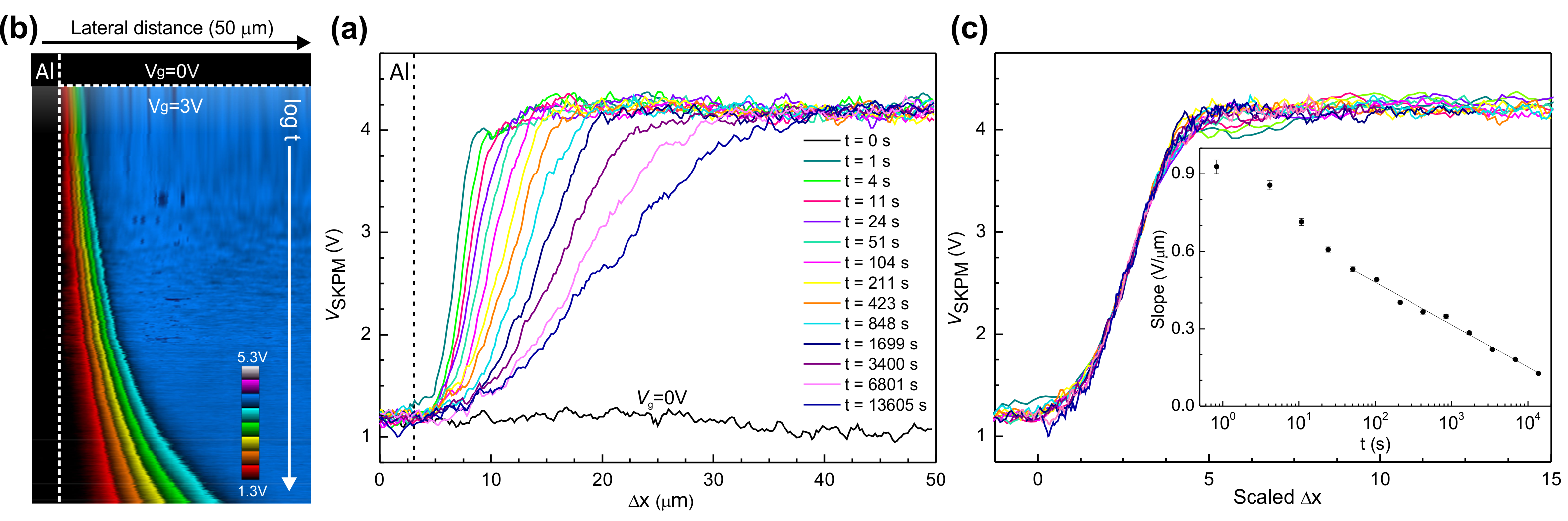
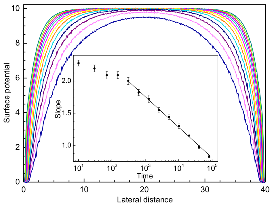
To study charging processes in the highly resistive granular Al samples, we first let the system relax to equilibrium for a very long time (typically 3 days) by fixing the two leads and the gate voltage at . Then, at some instant that is taken as the time origin, , the gate voltage is switched to and the surface potential evolution is monitored. Figure 2 (a) shows as a function of the lateral dimension (horizontal axis) and the time on a logarithmic scale (vertical axis) in a sample region close to one of the leads. Due to scanning size limitations, only one half of the channel is shown. However, it has been checked that a symmetric behavior take places at the other contact. When the gate voltage is switched from 0 to 3 V, the surface potential of the granular Al suddenly changes by the same amount, while the metal lead potential remains unaffected. Just after the voltage switching no current has yet been able to flow into the Al grain film. As a first approximation, at this instant the sample can therefore be considered as a dielectric. The SFM tip therefore “sees” the gate voltage through the granular Al and the SiO2 insulating layer (see Fig. 1). As time evolves, in order to reach a new equilibrium state, charge from the source and drain contacts enters into the granular aluminum to screen the . This is seen best in Fig. 2 (b) where lateral profiles at several times have been represented. These results are fairly independent of the value of the applied gate voltage. Note that while the time intervals between successive curves grow roughly exponentially, the change in slope between successive curves shown is similar. Thus, we observe an extremely slow charging behavior, which cannot be explained by a standard diffusive model with low conductivity.
To quantify the behavior of the central region of each curve has been fitted to a straight line
| (1) |
All the curves can be overlapped by plotting them as a function of the scaled variable as shown in Figure 2 (c). We first note the relatively high quality of the overlap. In second place, the symmetry between the two tails of the curves is also quite remarkable; we are dealing with an odd function with respect to the value at the center.
In the inset of Figure 2 (c), we plot the time dependence of the fitted slopes on a semilogarithmic scale. The roughly logarithmic dependence of the slopes with time is noticeable, a fact difficult to understand with uniform models of the conductivity and a clear indication of hopping processes with exponential distributions of resistances.
III.2 Memory effects
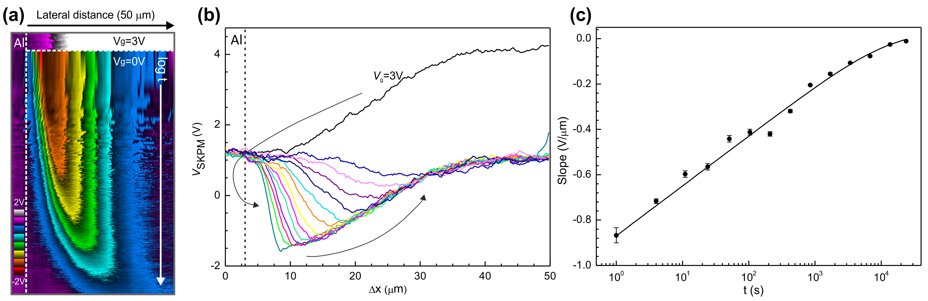
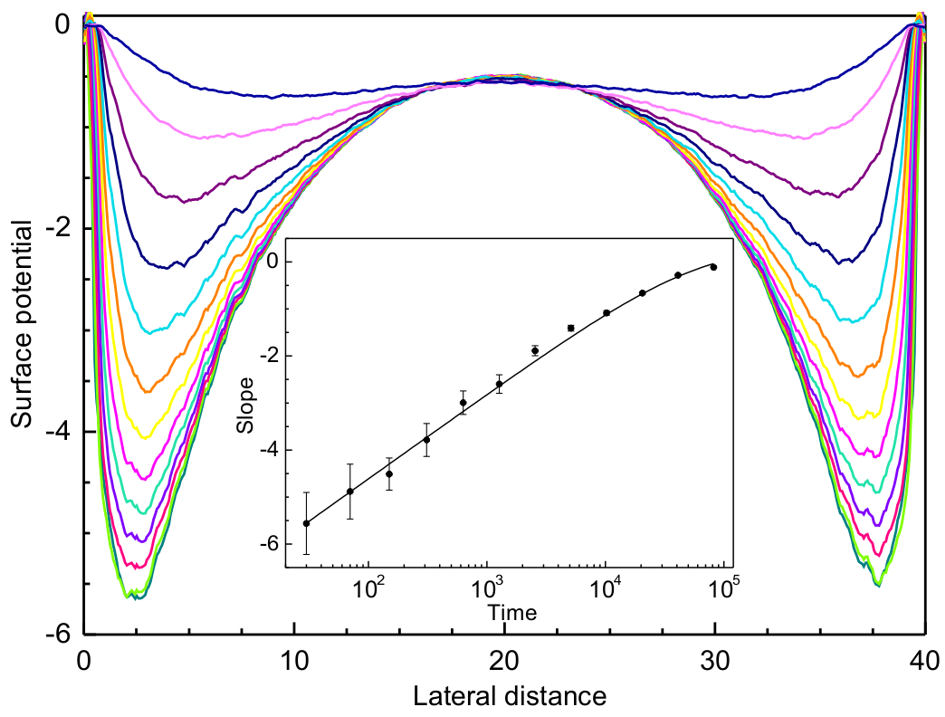
In our experiments, we have also monitored how the system relaxes back to equilibrium after the gate voltage is switched off. The results are shown in Fig. 3a where is plotted on a color scale versus the lateral distance (horizontal axis) and time on a logarithmic scale (vertical axis). They are also plotted in Fig 3b as a function of the lateral distance for several values of the time, with the time intervals between successive profiles increasing exponentially; the origin of time is taken as the instant in which the gate voltage is switched off.
As in the excitation phase, the curves for different times are roughly equally spaced for the exponentially spaced time intervals chosen. To quantify this fact, we measured the slope of the straight segment before the minimum value of for the different curves and the results are plotted versus time on a logarithmic scale in panel c of Fig. 3. Within the experimental error, the data follows a straight line with some bending at long times. The continuous curve corresponds to the standard relaxation behavior observed in systems showing logarithmic time evolutions Grenet2007 ; Amir15
| (2) |
where the ’waiting’ time is the time interval during which the gate has been kept at a certain voltage in the excitation phase (here about 5 h).
IV Theoretical analysis
A diffusion model (or, equivalently, a model with homogeneous conductivity) cannot explain even qualitatively the main features of these experimental results. The value of the diffusion constant establishes the time scale, but cannot get the wide distribution of relaxation times implied by a quasi logarithmic behavior. One can solve the diffusion problem in terms of modes characterized by a wavenumber , where are integers and is the distance between the leads. The characteristic time of a mode is adkins
| (3) |
resulting in a scaling form of the type . Each mode reduces proportionally at all positions with an exponential time dependence. The shapes of the potential curves predicted with this type of model are very different from those observed experimentally in the Al-grain samples discussed above. In particular, it is difficult to explain the almost constant value of the potential away from the leads when its value at closer positions has already changed noticeably.
IV.1 Model
The logarithmic dependence of the dynamical variables (inset in Fig. 2c, for example) is indicative of processes with rates depending exponentially on smoothly distributed random variables. Based on this hint and on the highly resistive nature of our samples we study a model suitable for hopping processes and adequate for numerical simulations. In order to keep the model as simple as possible we construct it in two dimensions.
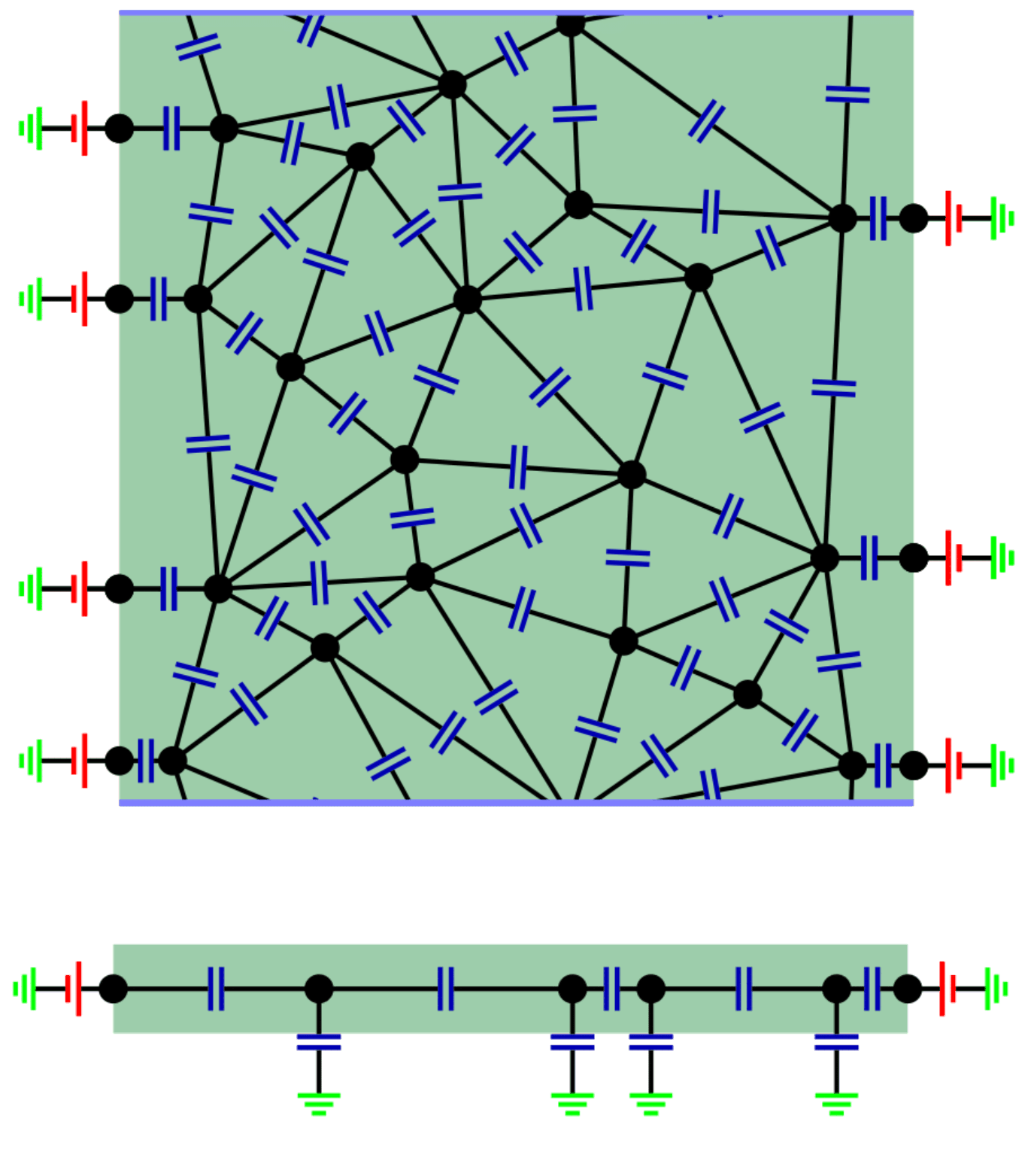
We consider a network model that consists on sites at random on a square sample of size and capacitors in the links joining nearest neighbor sites. Each site corresponds to a metallic grain (or set of metallic grains as explained bellow) and each capacitor to the capacitance between nearest neighbor grains Ortuno:2015 . A scheme of the network model is shown in Fig. 4. In order to perform a simulation as close as possible to the experimental setups and at the same time minimize finite size effects, we have included two leads at a potential in opposite sides of the sample and periodic boundary conditions in the other two sides. Sites near the leads are connected to them by capacitors. All sites are connected to the gate by capacitances , which take into account the field lines that go out of the system without ending in a nearby grain. The capacitances between sites take random values extracted from the distribution
| (4) |
We have taken (which sets our unit of energy) and . The choice of this particular distribution is not crucial, since it just introduces some small randomness in the capacitances and it has the property that the average value of the interaction between nodes is independent of Ortuno:2015 .
The charge on each site can only take integer values and is split between the plates of the capacitors connected to this site. Each capacitor has opposite charges on its two plates
| (5) |
where is the potential at site and the sum on runs over all sites, the two contacts and the gate. The charge on the leads can take any (fractional) value. We can rewrite the previous equation in matrix form
| (6) |
where is the capacitance matrix, defined as
| (7) |
Eq. (6) can also take care of the leads with a proper extension of the definition of the charge vector and of the capacitance matrix. In the leads, the potential is fixed and the charge is , where is the sum of all the capacitances connecting sites of the sample with the lead. It is convenient to define the following charge vector of dimension (see Ref. Ortuno:2015 for details of the model)
| (8) |
and to extend the definition of the capacitance matrix to include the conection with the leads.
We usually have an arrangement of charges and want to know the potential at each site. To solve this problem, we have to invert the capacitance matrix . This new matrix plays the role of an effective interaction between charges. The total energy of the system is directely obatained from
| (9) |
Given a set of charges, we calculate the energy through Eq. (9) and, following the hopping model of conductivity in localized systems, perform transitions of charge 1 between sites with probability proportional to POF13
| (10) |
where is the distance between sites and , the localization length, the energy difference due to the transition, Boltzmann constant and the temperature. We consider a temperature higher than the average charging energy of a site, but smaller than the applied voltage. Under these conditions, we expect that the factor of distance in Eq. (10) will be the crucial one. The energy factor would at most renormalize the percolation effects produced by the spatial factor, explained below.
The sites in our model can represent real metallic grains or effective ones formed by (possibly) many grains merging together by quantum tunneling in highly connected regions. This will just renormalize the energy scale towards smaller values and the time and spatial scales to larger values.
IV.2 Numerical results
We have performed Monte Carlo simulations with our network model changing systematically its parameters to try to reproduce as much as possible the experimental results. The key parameter of the model turns out to be the localization length. When it is larger than the typical site separation, the transition rates between sites are relatively homogeneous and the conduction mechanism can be modeled by diffusion. In the opposite case, hops of charges between close pairs are much more likely than hops between distant sites, the sample is very heterogeneous and conduction can be modeled by percolation theory POF13 . As we will see, most experimental features can be explained with the model parameters adjusted to the regime of percolation theory.
If the transition rate between two sites is given by Eq. (10) and the localization length verifies electron jumps between close sites are exponentially more likely that between distant sites. Following the standard approach to percolation in hopping systems POF13 , we consider that two sites are connected when several hops between them have been produced on average. Then at a given time sites with a separation smaller than
| (11) |
are connected, while those more separated remain unconnected. As explained above, we have assumed that the spatial factor in the hopping rate, Eq. (10), is the relevant one for our conditions. If sites are at random (or grain separations are roughly uniformly distributed), the exponential dependence of the hopping rate dominates the bond connectivity, and the proportion of bonds connected at a given time will be of the form
| (12) |
where is a constant that ensures the correct initial condition. Charge can penetrate in the sample along the clusters formed by connected pairs. According to percolation theory, the typical size of these clusters grows with time as POF13
| (13) |
is the critical percolation probability for the specific model considered, at which there is an extended connected cluster, and is the universal correlation length exponent for percolation in two dimensions.
As in Kelvin probe microscopy one adjusts the parameters to avoid as much as possible field lines between the point and the surface, the site potential of our model is directly related to the experimental surface potential. The results of a numerical simulation of the charging process are shown in Fig. 5. The average site potential is plotted as a function of the lateral distance to the electrode for several times and measured from the instant in which the gate voltage is switch on. Note that the time interval between successive curves grow exponentially. The localization length is , so conduction is well in the percolative regime. The overall shape of the curves are similar to the experimental results, but more importantly the time dependence of the slopes of the potential is roughly logarithmic, quite similar to the experimental behavior. In the inset of Fig. 5 we represent the slope of the surface potential versus time on a logarithmic scale. According to our model, the exponentially large distribution of characteristic times is due to the exponential dependence of the hopping rate on distance (and to a roughly uniform distance distribution). At low temperatures, the energy factor in the hopping rate can contribute further to the broadening of the times involved. As our experiments are at room temperature, we do not expect a significant contribution from the energy factor in the hopping rates. The gate voltage potential (10 for the results in Fig. 5) is chosen so that the charge in each grain is clearly higher than one. In this case the results are independent of the gate voltage, as in the experiments.
After the last time for which we measure the charging of the sample, we switch off the gate potential in our simulation and monitor again the time and spatial evolution of the site potential. The results are plotted in Fig. 6 for the same parameters as in the charging process, Fig. 5. The main features of the discharging curves are again reproduced by our simulations, although there are differences in the details. The overall logarithmic behavior is well reproduced as can be seen in the inset of Fig. 6, where the slopes of the first part of the curves are plotted versus time on a logarithmic scale. The continuous line corresponds to a fit to Eq. (2).
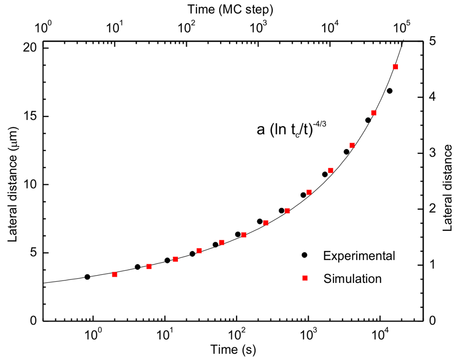
We can have a more restrictive test of our percolation model. If one pays attention to the experimental curves, Fig. 2, one can observe that they seem to accelerate (in a logarithmic scale) their approach to equilibrium at large time intervals. This is clearly evident in panel a where the initially almost straight lines become bent at the bottom of the figure. We interpret this as a sign that, at the largest times involved in our experiments, we are close to reaching percolation, so that the size of the connected clusters increases faster, according to Eq. 14, as the system approaches critical percolation and the whole sample would be connected. To quantify this observation we plot the lateral distance of the point at which the voltage is equal to the mean between the lead and the gate voltages as a function of time. In Fig. 7, we show the results for both the experimental data (black points, left axis in m) and the numerical simulations (red points, right axis in grains separation). The horizontal time axis is in seconds for the experimental points and in Monte Carlo sweeps for the simulation results, and it has been shifted for the simulation results to achieve a maximum overlap between both set of points. The line is a fit of the experimental data to the analytical expression of the typical cluster size in percolation theory
| (14) |
To derive this equation, we have taken into account the time dependence of the connecting probability, Eq. (12), is the critical time needed to reach percolation, and is the correlation exponent in two-dimensional percolation. The quality of the fit and the analogy between experimental and numerical simulation results is strong indication of the percolative character of the charging process.
V Conclusions
We have repeated the previous measurements for other samples with different resistances. If the samples are conducting enough so that its conductivity can be measured, the processes studied here take place at a fast scale and our set up is not fast enough to detect intermediate processes. If the samples are much more resistive than the ones analyzed here, we do not see any dynamics. As resistance varies exponentially with grain separation, we can only measure a relatively narrow range of metallic concentrations.
In principle, this technique can be adapted to measure the conductivity of highly resistive samples for which standard macroscopic methods are not sensitive enough to determine it. We now intend to apply the SKPM technique to study at the nanometer scale the glassy effects reported in the conductance of several disordered insulators.Grenet2007 ; Ovadyahu2007 ; HaEi12 ; Grenet2010 . Indeed in some of them, in the appropriate resistance range, these occur up to room temperature.Eisenbach2016 ; Delahaye2014 ; granular The technique can be very useful to analyze memory effects, and combined with conductance measurements, may shine light on the mechanisms involved.
Acknowledgements
The work was supported by the Spanish MINECO Grants No. FIS2015-67844-R, ENE2013-48816-C5-1-R, ENE2016-79282-C5-4-R, and CSD2010-00024, and by Fundación Séneca grant 19907/GERM/15.
References
- (1) Vaknin, A., Ovadyahu, Z. & Pollak, M. Nonequilibrium field effect and memory in the electron glass, Phys. Rev. B 65, 134208 (2002).
- (2) Grenet, T., Delahaye, J., Sabra, M., and Gay, F., Anomalous electric-field effect and glassy behaviour in granular aluminium thin films: electron glass?, Eur. Phys. J. B, 56, 183-197 (2007).
- (3) Ovadyahu, Z., Relaxation Dynamics in Quantum Electron Glasses, Phys. Rev. Lett. 99, 226603 (2007).
- (4) Havdala, T. Eisenbach, A. And Frydman, A., Ultra-slow relaxation in discontinuous-film based electron glasses, Europhys Lett, 98, 67006 (2012).
- (5) Grenet, T And Delahaye, J. Manifestation of ageing in the low temperature conductance of disordered insulators, Eur. Phys. J. B, 76, 229-236 (2010).
- (6) Pollak, M. And Ovadyahu, Z., A model for the electron glass, Surf. Sci. Rep. 92, 283-287 (2006).
- (7) Pollak, M., Ortuño, M. And Frydman, A. The Electron Glass (Cambridge University Press, Cambridge, 2013).
- (8) Amir, A. And Oreg, Y. And Imry, Y., On relaxations and aging of various glasses,.Proc. Nat. Acad. Sci. 109, 1850-1855 (2015).
- (9) Eisenbach, A., Havdala, T., Delahaye, J., Grenet, T.,Amir, A. and Frydman, A, Glassy Dynamics in Disordered Electronic Systems Reveal Striking Thermal Memory Effects, Phys. Rev. Lett. 117, 116601 (2016).
- (10) Delahaye, J., Grenet, T., Marrache-Kikuchi, C.A., Drillien, A.A. And Berge, L, Observation of thermally activated glassiness and memory dip in a-NbSi insulating thin films, Europhys Lett, 106, 67006 (2014).
- (11) http://www.um.es/bohr/files/moo/SlDelahaye.pdf
- (12) Ortuño, M.,Escasain, E.,Lopez-Elvira, E., Somoza, A.M., Colchero, J. And Palacios-Lidon, E., Conducting polymers as electron glasses: surface charge domains and slow relaxation, Sci. Rep. 6, 21647 (2016).
- (13) Orlyanchik, V. and Ovadyahu, Z., Electron glass in samples approaching the mesoscopic regime, Phys. Rev. B 75, 174205 (2007).
- (14) Delahaye, J., Grenet, T. and Gay, F., Coexistence of anomalous field effect and mesoscopic conductance fluctuations in granular aluminium, Eur. Phys. J. B, 65, 5-19 (2008).
- (15) Benjamin, J. D., Adkins, C. J. and Van Cleve, J. E., Resisitive inhomogeneity in discontinuous metal films, J. Phys. C: Solid State Phys. 17, 559 (1984).
- (16) Adkins, C. J. et al., Potential disorder in granular metal systems: The field effect in discontinuous metal films, J. Phys. C: Solid State Phys. 17, 4633 (1984).
- (17) Tsigankov, D. N. & Efros, A. L. Variable Range Hopping in Two-Dimensional Systems of Interacting Electrons, Phys. Rev. Lett. 88, 176602 (2002).
- (18) Somoza, A. M., Ortuño, M. and & Pollak, M. Collective variable-range hopping in the Coulomb gap: Computer simulations, Phys. Rev. B 73, 045123 (2006).
- (19) M. Ortuño, A. M. Somoza, V. M. Vinokur, and T. I. Baturina, Electronic transport in two-dimensional high dielectric constant nanosystems, Sci. Rep. 5, 9667 (2015).
- (20) Palacios-Lidon, E., Perez-Garcia, B. And Colchero, J., Enhancing Dynamic Scanning Force Microscopy in air: As close as possible, Nanotechnology 20, 085707 (2009).
- (21) Horcas, I., Fernandez, R., Gomez-Rodriguez, J.M., Colchero, J., Gomez-Herrero, J. And Baro, A.M. WSXM: A software for scanning probe microscopy and a tool for nanotechnology, Rev. Sci. Instrum. 78, 013705 (2007).
- (22) Palacios-Lidon, E., Abellan, J., Colchero, J., Munuera, C. And Ocal, C., Quantitative electrostatic Force Microscopy on heterogeneous nanoscale samples, Appl. Phys. Lett. 87, 154106 (2005).