CoFFEE: Corrections For Formation Energy and Eigenvalues for charged defect simulations
Abstract
Charged point defects in materials are widely studied using Density Functional Theory (DFT) packages with periodic boundary conditions. The formation energy and defect level computed from these simulations need to be corrected to remove the contributions from the spurious long-range interaction between the defect and its periodic images. To this effect, the CoFFEE code implements the Freysoldt-Neugebauer-Van de Walle (FNV) correction scheme. The corrections can be applied to charged defects in a complete range of material shapes and size: bulk, slab (or two-dimensional), wires and nanoribbons. The code is written in Python and features MPI parallelization and optimizations using the Cython package for slow steps.
keywords:
Charged defects , Defect formation energy , Density Functional Theory , Eigenvalue corrections , electronic structurePROGRAM SUMMARY
Program Title: CoFFEE
Program obtainable from: http://www.physics.iisc.ernet.in/~mjain/pages/software.html
Journal Reference:
Catalogue identifier:
Licensing provisions: Open source BSD License
Programming language: Python
Computer: Any computer with Python installed. The code has been tested with Python2.7 and Python3.6.
Operating system: Unix/Linux/Windows
RAM: 5-1000 MB (dependent on system size)
Keywords: Density Functional Theory, Defect formation energy,
Charged defects, Eigenvalue corrections, Electronic Structure, GW
Classification: 7.1, 7.3
External routines/libraries: numpy, scipy, mpi4py, matplotlib
Nature of problem: Most electronic structure codes based on Density Functional Theory
use periodic boundary conditions. This leads to spurious electrostatic interactions during simulation of
charged defects, which affects the computed defect formation energy and the defect eigenvalue.
Solution method: We implement the Freysoldt-Neugebauer-Van de Walle (FNV) correction scheme to correct
the defect formation energy and eigenvalues. Our implementation can be applied to charged defects in 3D bulk materials
as well as materials having 2D and 1D geometries.
Running time: 1-600 minutes (depends on the number of processors and system size)
1 Introduction
Point defects, ubiquitous in materials, influence their electrical and optical properties. First principles electronic structure calculations have proven to be vital in understanding and predicting the role of defects [1, 2, 3, 4, 5, 6, 7, 8, 9, 10, 11, 12, 13, 14, 15, 16, 17, 18]. Defect engineering to enhance or suppress certain characteristics of materials often rely on such simulations for inputs [19, 20, 21, 22, 23, 24, 25].
Intrinsic point defects in materials are generally found in low concentrations, about one in a million atoms in 3D solids to one in a thousand atoms in 2D materials. Simulations thus attempt to study isolated defects in materials. However, a large number of first principles calculation codes based on Density Functional Theory (DFT) employ periodic boundary conditions. As a result, in order to simulate and understand isolated defects, super cells are constructed. The size of the super cell is chosen to minimize the overlap of the defect wavefunction with its periodic image in neighboring cells [1, 26, 27, 28, 29, 30, 31]. The computed formation energy of non-shallow neutral defects in such calculations is found to converge quickly with the super cell size.
Charged point defects are simulated by artificially introducing a compensating uniform background charge to avoid the divergence in the electrostatic energy. The formation energy of charged defects show slow convergence with super cell size due to the Coulomb interaction between the defect charge and its periodic images. The super cell sizes necessary to completely overcome these spurious defect-defect interactions are computationally intractable. The defect energy levels in the gap are also affected similarly, and shows slow convergence with super cell size [27, 32, 33]. Furthermore, since the uniform background charge is artificially introduced, an absolute reference for the electrostratic potential is undefined. The potential in the defect supercell thus needs to be aligned with the bulk potential, in accordance with the chosen reference of the Fermi level with respect to the bulk VBM.
Several a posteriori correction schemes have been developed to tackle this issue [26, 28, 34, 35, 29, 36, 37]. Most of the correction schemes involve solving the Poisson equation for a model system, and aligning of potentials, to derive the correction to the formation energy. In particular, the scheme proposed by Freysoldt, Neugebauer and Van de Walle (FNV) has gained a lot of popularity owing to its consistency in deriving accurate corrections for charged defects in numerous materials [26]. This scheme has been extended to low-dimensional systems as well, and shown to perform well [38, 39, 40, 41, 42, 43, 44]. However, a generalized correction scheme implementation that works with bulk as well as low-dimensional systems is absent in the various DFT packages, or as an independent package [45, 46]. The recent independent packages are restricted to compute the corrections for charged defects in bulk systems alone [45, 46].
We present a complete electrostatic corrections package, CoFFEE: Corrections For Formation Energy and Eigenvalues for charged defect simulations. The package is applicable to charged defects in materials ranging bulk solids, interfaces, surfaces/slabs, two-dimensional (2D) materials, nanowires and nanoribbons. These materials can be classified according to the number of periodic directions, into 3D (bulk) , 2D (slabs, 2D materials) and 1D (nanowires, nanoribbons) systems. We implement a generalized Poisson solver based on the FNV correction scheme with a gaussian model charge distribution. Tools to compute the potential alignment terms in the FNV correction scheme are also provided with the package. The code is written entirely in Python [47]. We use Message Passing Interface (MPI) to parallelize the code and Cython [48] to accelerate slow steps. Our implementation can be used alongside any DFT package to obtain an a posteriori correction for the formation energy and the defect level position in the gap, for the charged defect being simulated.
2 Theoretical framework
The formation energy of a neutral defect in a material is given by:
| (1) |
where is the Fermi level, is the total energy of a system containing a neutral defect with atom positions at . represents the total energy of a pristine super cell of the same size. refers to the number of atoms of type added (positive) or removed (negative) from the pristine system, and is the atom’s chemical potential [27]. The neutral defect formation energy needs no electrostatic correction term due to the absence of any long range electrostatic defect-defect interactions.
The formation energy of a defect in charge state is given by [27]:
| (2) |
The first term on the right hand side is the total energy of a system containing a defect in charge state q with the requisite finite-size electrostatic correction (described below). The formation energy is now a function of the Fermi level in the system, , with respect to the pristine valence band maximum (VBM), .
| (3) |
is a potential alignment term found by comparing the electrostatic potentials from a pristine calculation and far from the defect in a neutral defect calculation.
2.1 FNV correction scheme
The electrostatic correction term, , is incorporated to correct the spurious interaction between the defect charge and its periodic images. In the FNV scheme, this term is given by [27, 26]:
| (4) |
where is obtained from a model calculation. It involves solving the Poisson equation using a model charge distribution, , and model dielectric profile under periodic boundary conditions to obtain the potential, [27, 26]. is then given by:
| (5) |
where the integral is over the super cell volume, . is evaluated for larger super cells and extrapolated to obtain . Performing larger super cell calculations within this model is computationally inexpensive compared to a DFT calculation on such systems. accounts for the long range interactions. The dependence of on the model charge distribution is eliminated by the second term in 4. is a potential alignment term found by comparing the model potential to the DFT difference potential:
| (6) |
2.2 Model calculation
The model super cell calculation for involves solving the Poisson equation for the periodic model potential, [39, 38, 42]:
| (7) |
where is the dielectric tensor profile of the material, is the model charge distribution. The dielectric tensor can be obtained using Density Functional Perturbation Theory (DFPT) [49, 50]. Eqn 7 can be effectively solved in the reciprocal space [39, 38, 42]:
| (8) |
where are the diagonal terms of the dielectric tensor. is set to zero, which is equivalent to introducing a uniform, neutralizing background charge. The number of G vectors used in the calculation is determined by an energy cut off.
As one is interested in the long range corrections, in the material can be assumed to have no spatial profile; however, in general, it is a 33 tensor. In a 3D bulk system with an isotropic dielectric, can be obtained from Eqn 8 as:
| (9) |
For slab or two-dimensional systems, on the other hand, the dielectric tensor, while not having any profile inside the material, would still have a spatial profile in the aperiodic direction, say [39, 38].
where and is the dielectric profile for the in-plane dielectric constants and and is the dielectric profile for the out-of-plane dielectric constant of the material.
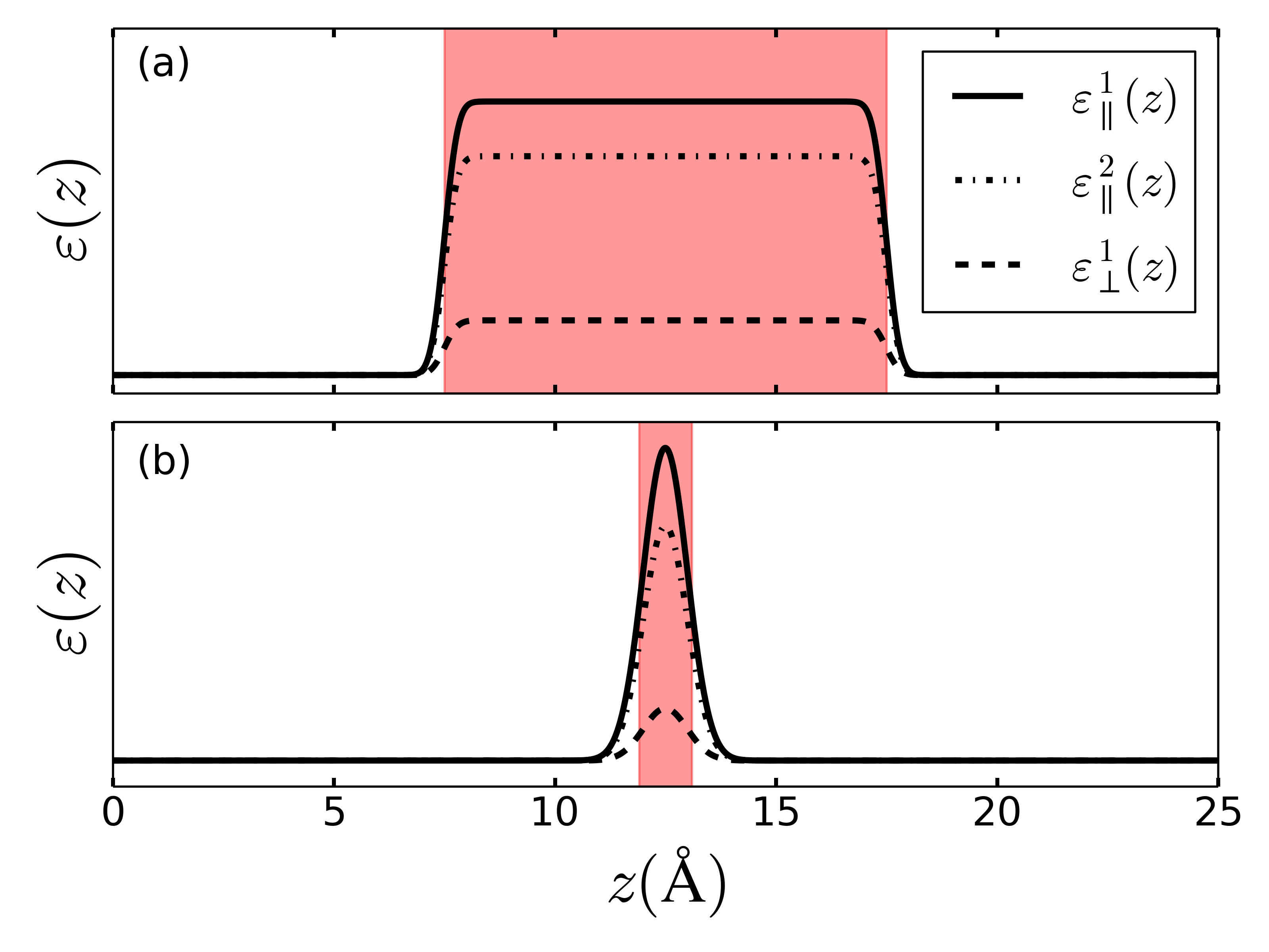
For slab systems or a 2D material with more than one atom thickness, like transition metal dichalcogenides, phosphorene, etc., the dielectric profile used is of the form, [39, 38]:
| (10) |
where and are the edges of the slab in the -direction in the simulation cell. A parameter, , is used with the error function (erf) to smoothen the profile at the slab edges. is the dielectric constant of the material, found using DFPT [39]. is the dielectric constant of the space surrounding the material, set to 1 for vacuum. A sample slab profile is shown in Fig 1 (a). For a 2D material with one atom thickness, like Boron Nitride (BN), Silicon Carbide (SiC), graphene, etc., the dielectric profile used is a gaussian to mimic the planar-averaged charge density of the material in the -direction. A sample profile is shown in Fig 1 (b).
For slab or 2D systems, Eqn 8 can then be written as:
| (11) |
The average potential, , is set to zero, to introduce a neutralizing bakground charge.
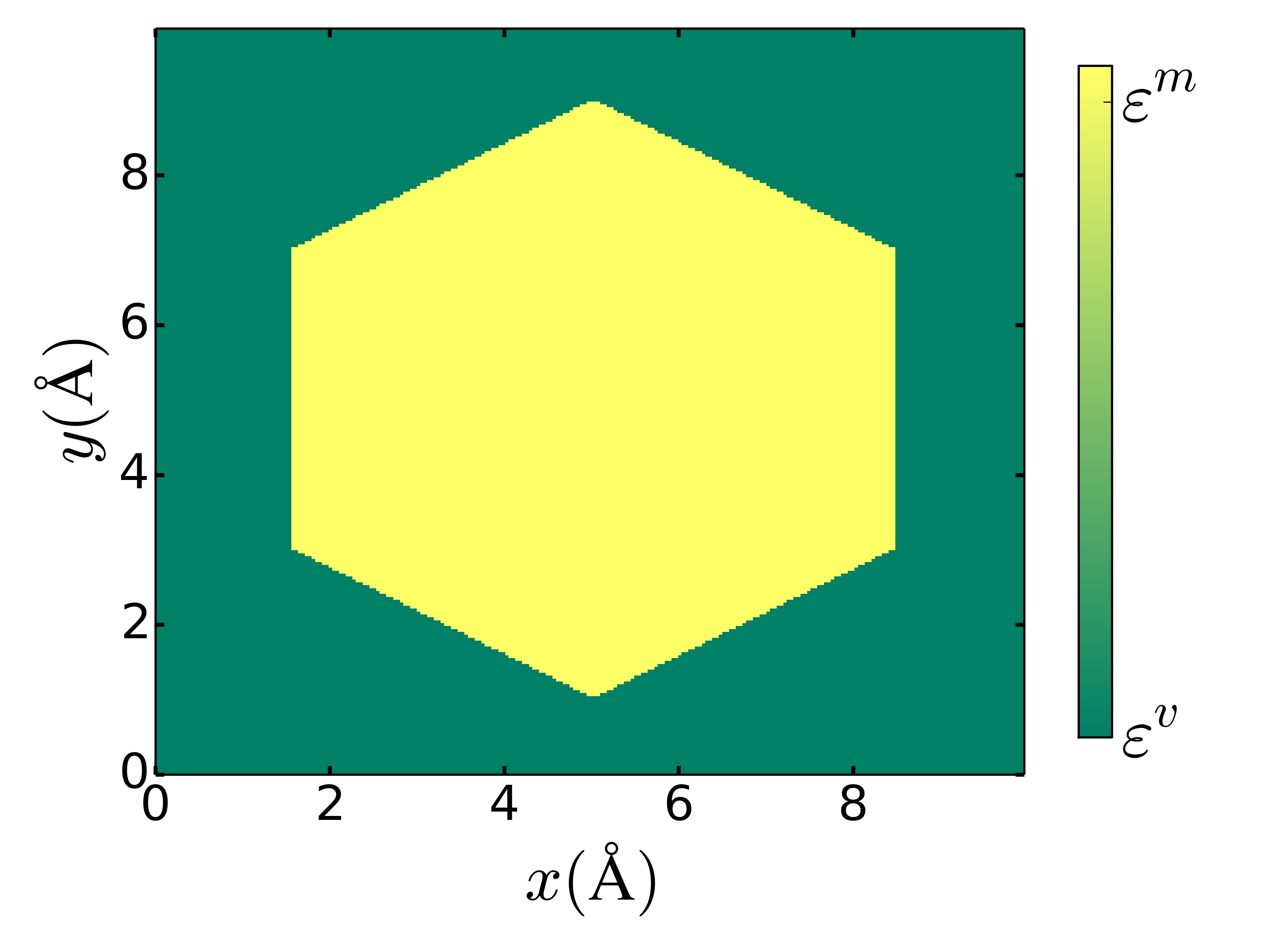
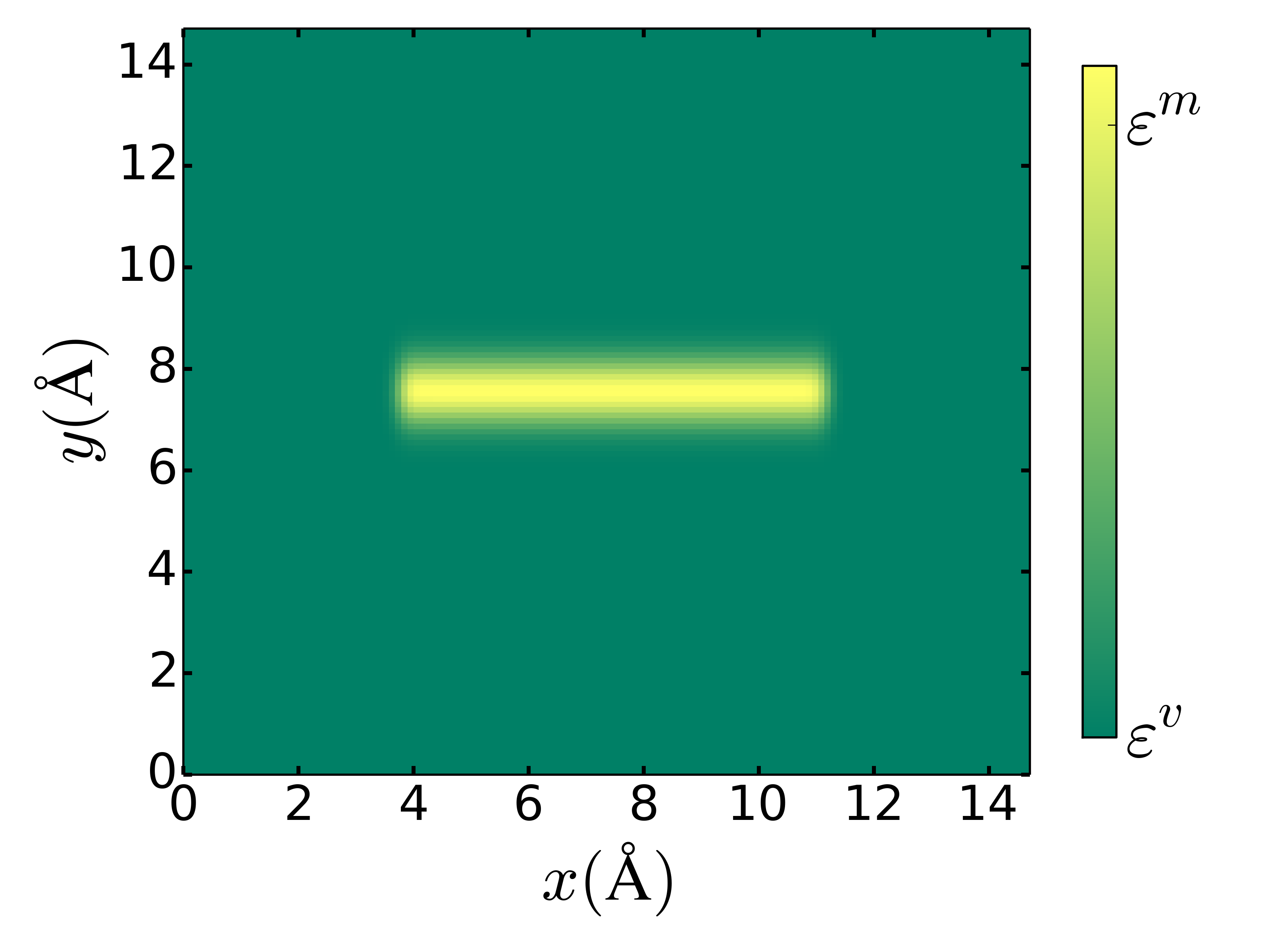
For a quasi-1D system like nanowires or nanoribbons, with perodicity along the direction, the dielectric tensor profile is of the form [42] :
where is the profile for the dielectric constant perpendicular to the wire and is the profile for the dielectric constant along the wire. A sample profile for a silicon nanowire along the [111] direction is shown in Fig. 2. The wire, oriented along the direction, has a hexagonal cross-section [42]. The profile is constructed such that the points inside the wire have the dielectric constant of the material, , and the points outside have . A sample profile for a BN nanoribbon is shown in Fig. 3. The profile is constructed to mimic the electron charge density of the material by combining a slab like profile (Eqn 10) along the width of the nanoribbon and a gaussian along the out-of-plane direction. Eqn 8, for 1D systems, can then be written as [42]:
| (12) |
We set here, to introduce a neutralizing background charge.
2.3 Defect eigenvalue correction
The defect eigenvalues, like the formation energy, show slow convergence with the super cell size [32, 33]. The correction to the eigenvalue is given by [33]:
| (13) |
where is the FNV correction term, Eqn 4. The correction is negative for positively charged defects and positive for negatively charged defects. Defect level corrections are crucial in studying defects using the DFT+GW formalism [32, 33, 2, 3, 1] and also in interpreting absorption experiments.
3 Test Systems
We show the performance of our code in correcting the formation energies and defect levels in the following systems:
-
1.
Bulk: Carbon vacancy in diamond in charge state -2, .
-
2.
2D: Sulfur vacancy in monolayer MoS2 in charge state -1, .
-
3.
1D: Boron vacancy in BN nanoribbon in charge state -1, .
All the DFT calculations are performed using the plane-wave, pseudopotential package, Quantum Espresso [51]. We perform simulations on a range of super cell sizes and compare the extrapolated formation energy and defect level (to the isolated limit) with the corrected formation energy and defect level.
3.1 Vacancy in diamond,
We perform DFT calculations on different cubic super cell sizes with number of C atoms ranging from 64 to 1024. We use norm-conserving pseudopotentials and the LDA exchange correlation functional [52]. The wavefunctions are expanded in plane-waves upto an energy cut off of 60 Ry. For the 64 atom, 222 super cell, a k-point sampling of 555 was used. An equivalent sampling is used for the other super cell sizes. We did not include any atomic relaxations.
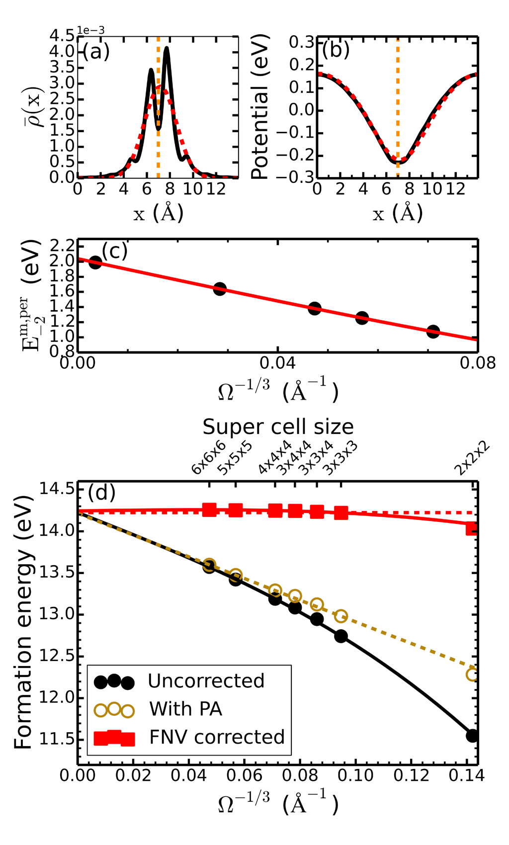
The model calculation is performed using the CoFFEE code, solving Eqn 9. The defect is modelled with a gaussian of width 2.6 bohr, a dielectric constant of 5.76 and a plane wave energy cut off of 16 Ry. Fig. 4 (a) shows the defect wavefunction charge density, , and the model charge density. For bulk systems, it is not necessary that the width of the Gaussian model charge match the defect wavefunction charge density. It suffices if the width is appropriately small to keep the model charge inside the cell. Note also that the plane wave energy cut off required to converge the model calculation is inversely proportional to the width of the Gaussian. Fig. 4 (c) shows the extrapolation of the model energy, (Eqn 5), with super cell size, . The energy is fit with a polynomial of the form:
| (14) |
here corresponds to the isolated model energy, . The fitting parameters here are: , and . The lattice correction is then given by: (Eqn 4). Fig. 4 (b) compares the planar averaged model potential and the DFT difference potential which contribute to the potential alignment term, (Eqn 6) for a 333 super cell. The defect in this calculation is at the center of the cell. The model potential matches well with the DFT difference potential far from the defect, leading to a very small correction. On the other hand, the potential alignment term, in Eqn 2, which compares the potential far from the neutral defect to the pristine, has a substantial contribution.
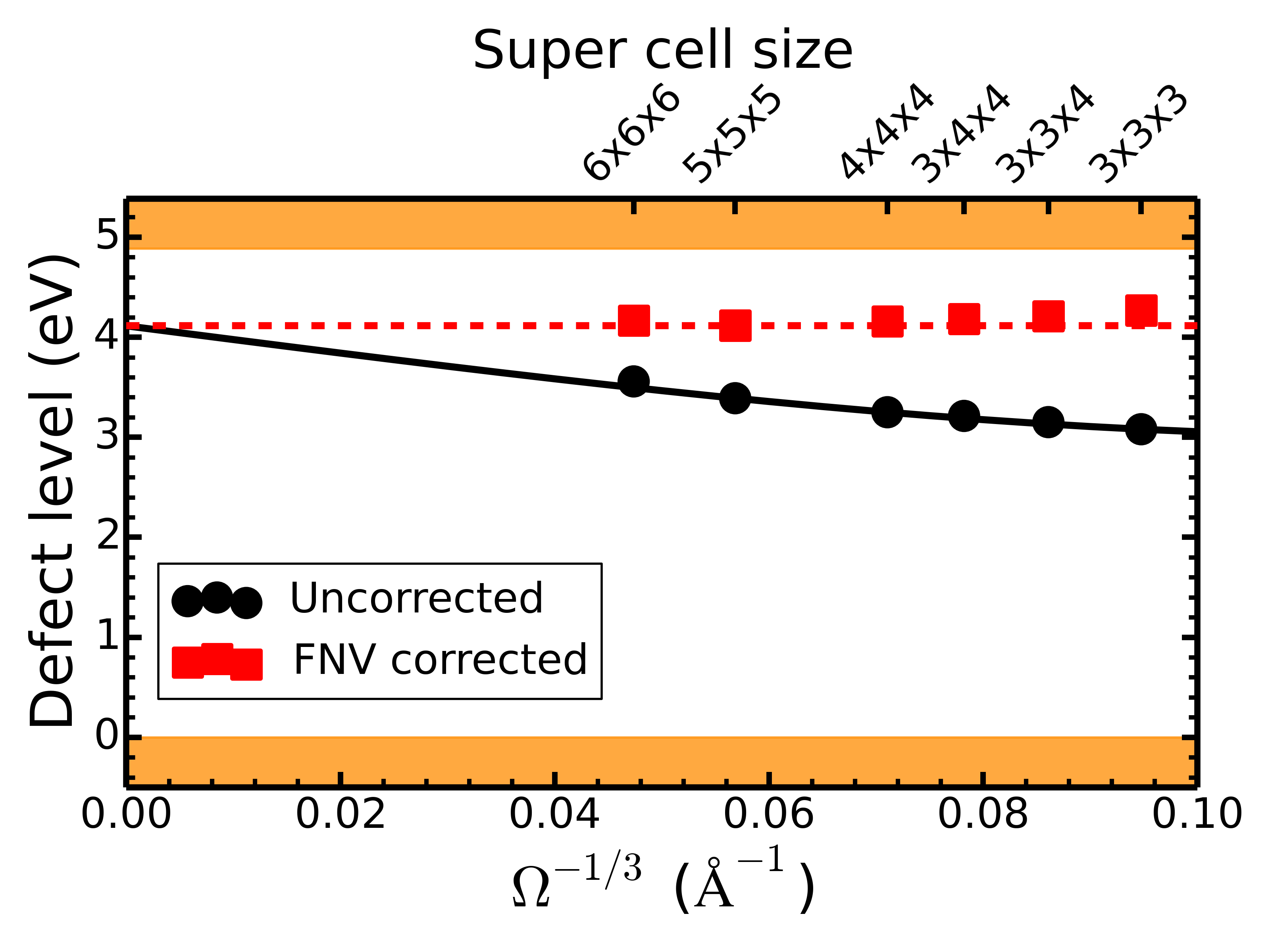
The uncorrected formation energy of for various supercell sizes is fit using Eqn 14 to extrapolate to the isolated limit as shown in Fig. 4 (d). The chemical potential of carbon is taken from bulk diamond. The FNV corrected formation energy shows good agreement with the extrapolated value for super cell sizes larger than 222. The correction scheme performs well when the defect wavefunction is localized well within the super cell; this is not the case with the 222 super cell. The defect level accomodating the -2 charge is shown in Fig. 5 with respect to the pristine VBM eigenvalue in the charged super cell. It shows a similar scaling with super cell size and is corrected using Eqn 13.
3.2 Vacancy in monolayer MoS2,
We study sulfur vacancies in monolayer MoS2 to demonstrate the electrostatic corrections in 2D or slab systems. The DFT calculations are performed using PAW pseudoptentials [53], PBE scheme for the exchange correlation functional [54]. A wavefunction cut off of 50 Ry, and charge density cut off of 500 Ry is used. We perform calculations on four super cell sizes: , for = 4, 5, 6 and 8. The refers to the scaling of the cell dimension. It has been reported that scaling just the in-plane supercell, keeping the amount of vacuum fixed, leads to a divergence in the model energy [38]. We hence uniformly scale the vacuum with the in-plane super cell. For , the vacuum thickness is and thickness of MoS2 is . The k-point sampling for these is chosen to effectively sample the unit cell Brillouin zone with a grid better than 12121. The atoms are relaxed to their equilibrium positions such that the force on each atom is eV/Å.
The model calculation is performed solving Eqn 11. The dielectric profile is chosen as in Eqn 10, with in the direction parallel to the material and in the perpendicular direction. The smoothening parameter, s, is chosen to be 0.38 bohr. The dielectric constants are determined using DFPT as prescribed in reference [39]. The plane wave energy cut off is set to 30.0 Ryd. The defect is modelled with a Gaussian of width 1.9 bohr as shown in Fig. 6 (a). It is important here to choose a Gaussian width that mimics the defect charge density. Choosing a width too large that spills beyond the gray shaded region in Fig. 6 (a) would affect the results. The defect wavefunction charge density can be fit to a Gaussian using the script g_fit.py supplied with the CoFFEE code.
Fig 6 (b) compares the planar averaged model potential with the planar averaged DFT difference potential, , for the supercell. The DFT difference potential used here is from unrelaxed calculations and shows good agreement with the model potential far from the defect. Fig 6 (c) shows the variation of the model electrostatic energy with two different scalings of the super cell size: and . For super cell scaling, the vacuum thickness is 1.6 times larger than that of scaling. The interaction between the periodic charges is unscreened in the out-of-plane direction, and screened by the material in the in-plane direction. The model energy is thus strongly dependent on the vacuum thickness, for small super cell sizes. As expected, at the infinite limit (), the two scalings extrapolate to the same value. The model scaling plots clearly do not follow a simple fit as in the case of bulk solids due to the spatially varying dielectric profile. The energy is fit with a polynomial of degree five in : [39]. The isolated model energy is given by , and the lattice correction is given by: . The fitting parameters, for scaling, are found to be: , , , , and .
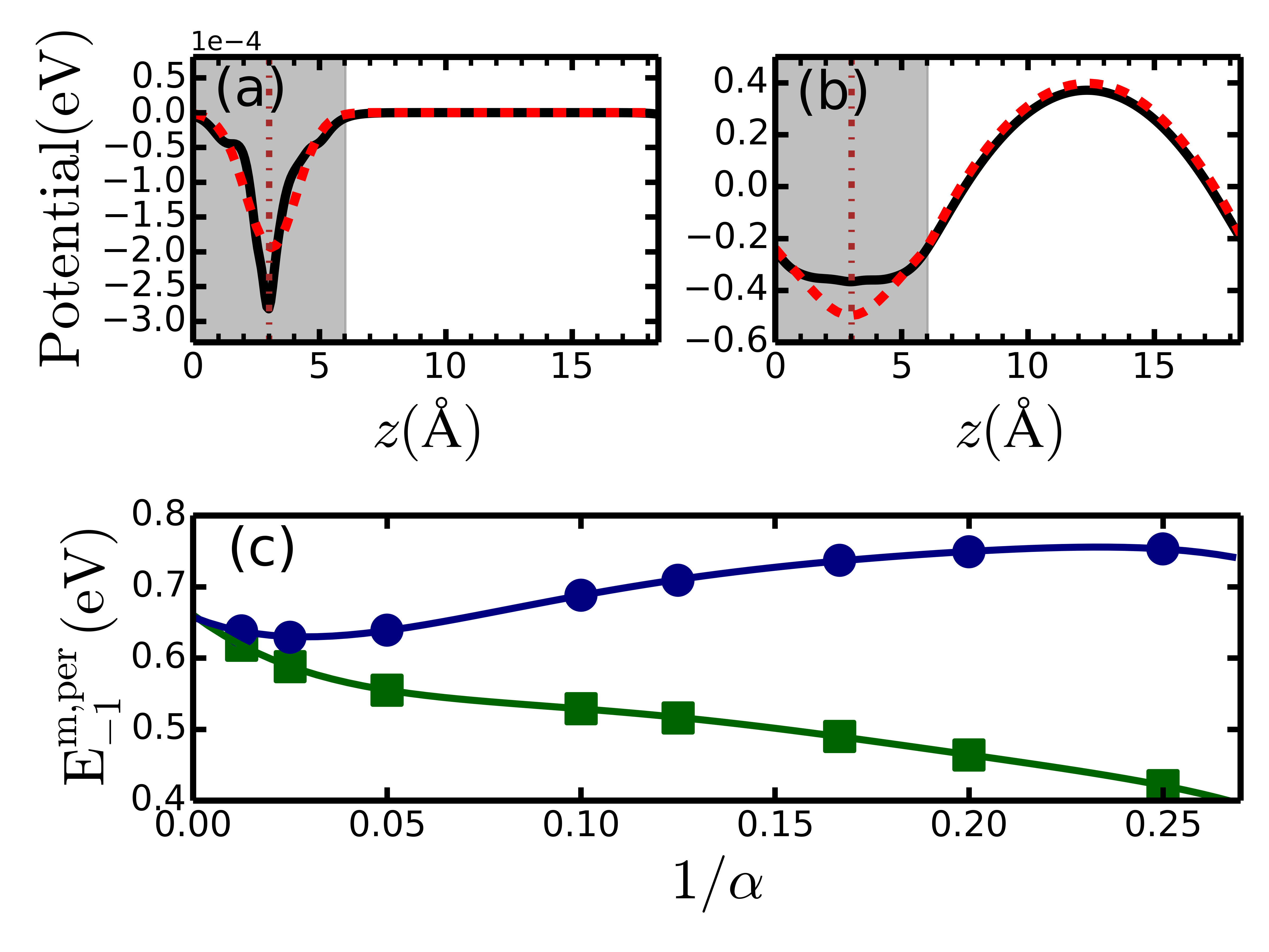
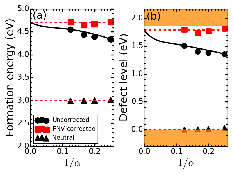
Fig 7 (a) shows the scaling of the uncorrected formation energy of neutral S vacancy, , and -1 charged S vacancy, , as a function of super cell size. The chemical potential of sulfur is taken from the cyclo-S8 allotrope of sulfur. The neutral vacancy formation energy is well converged and shows no scaling with system size. The scaling of the charged vacancy formation energy is fit with a polynomial of the form [39]: . The additional terms are necessary to capture the scaling of the potential alignment term with system size. and are found to be 4.71 and -8.69 respectively. The FNV corrected formation energy shows excellent agreement with the extrapolated value for all the super cell sizes considered. Fig 7 (b) shows the dependence of the defect level accomodating the -1 charge with system size. The uncorrected values are fit with a polynomial of the form: . The corrected eigenvalues are in good agreement with the extrapolated value.
3.3 Vacancy in BN nanoribbon,
To show the application of the code for 1D systems, we study B vacancy in a BN nanoribbon of thickness 13.39 Å[13]. We perform calculations on three super cell sizes: (12.311), for . For , the simulation cell dimensions are 15, 35 and 15, in the , and directions repectively. The direction is the periodic direction. A vacuum of 15 and 22 has been introduced in the out-of-plane direction and lateral direction. The thickness of the ribbon is fixed in these cell sizes, with the number of atoms in the periodic direction and the vacuum padding scaling with . The ribbon is passivated on either side with H atoms. Ribbon in super cell with a B vacancy is shown in Fig 8 (a). The DFT calculations are performed using norm conserving pseudopotentials and the PBE scheme is used for the exchange correlation functional [54]. A plane wave energy cut off of 70 Ry is used for the wavefunctions. The Brillouin zone is sampled with a 112 grid for and with the point for . We relaxed the atoms in the super cell containing the defect until the force on each atom is eV/Å.
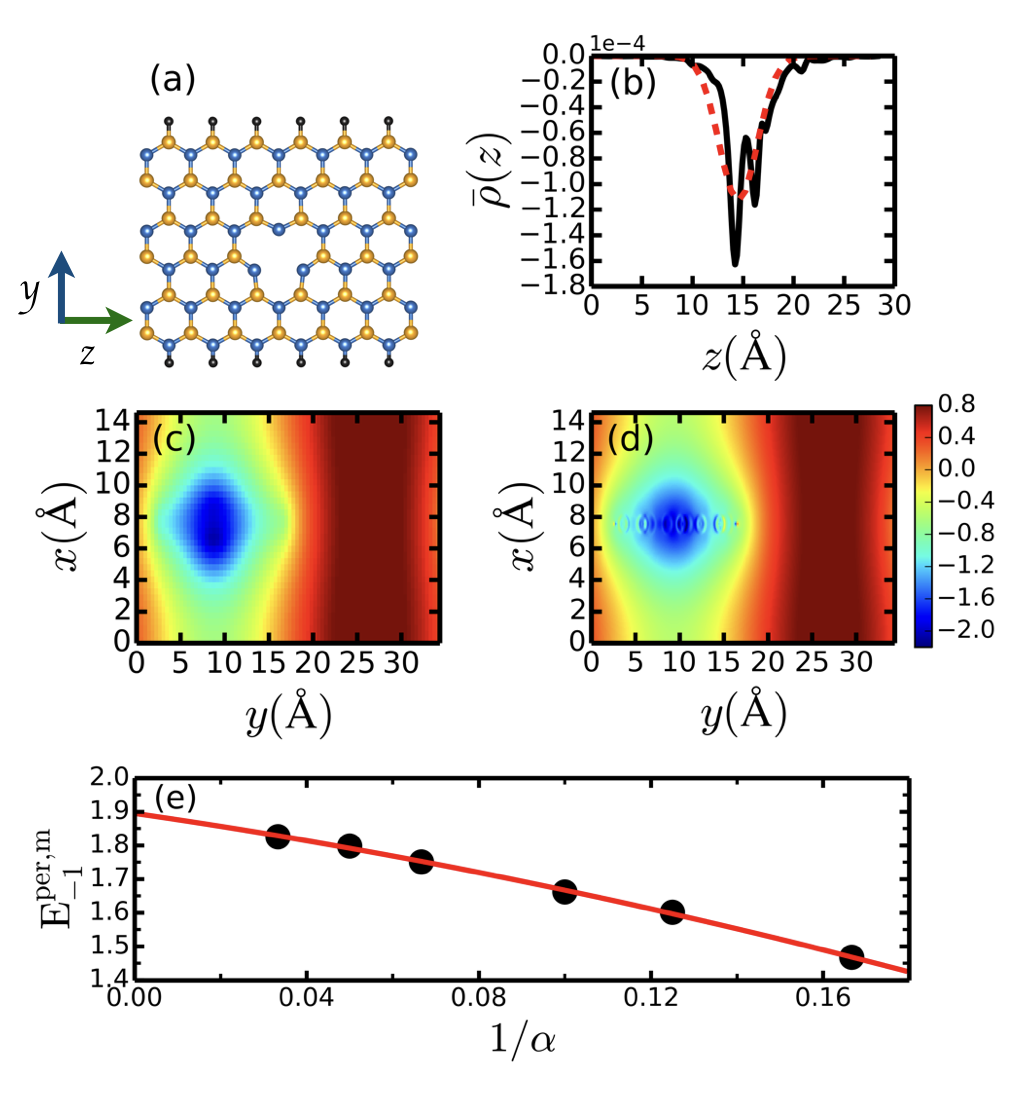
For the model calculation, we use a dielectric profile as shown in Fig 3. A slab like profile, similar to the one used for MoS2, is used along the width of the nanoribbon and a gaussian profile in the out-of-plane, direction. The width of the slab is taken to be that of the width of the nanoribbon, with a smoothening parameter of 0.37 bohr. The gaussian width is taken to be 0.86 bohr, chosen to mimic the electron charge density in that direction. used is 2.9 along the direction and 12 along the other two directions. These are computed from DFPT calculations on a monolayer BN sheet. We use a gaussian model charge with width 1.89 bohr and integrated charge -1. The planar averaged model charge and the defect wavefunction charge density are shown in Fig. 8 (b). The calculation is performed with a plane wave energy cut off of 16.0 Ry. Fig 8 (e) shows the scaling of the computed as a function of 1/. The points are fit with a third degree polynomial in : . then corresponds to the isolated model energy, , and the lattice correction is given by: . The fitting parameters are found to be: , , and . The potential alignment terms, and , are calculated by comparing the potentials in the out-of-plane, direction, far from the defect. Both these terms are found to be small ( 20 meV). Fig 8 (c) and (d) show the DFT difference potential in Eqn 6 and the model potential, respectively, for super cell size. The defect is at (x, y) = (7.5, 9) in the figure. The model potential matches well with the DFT difference potential far from the defect.
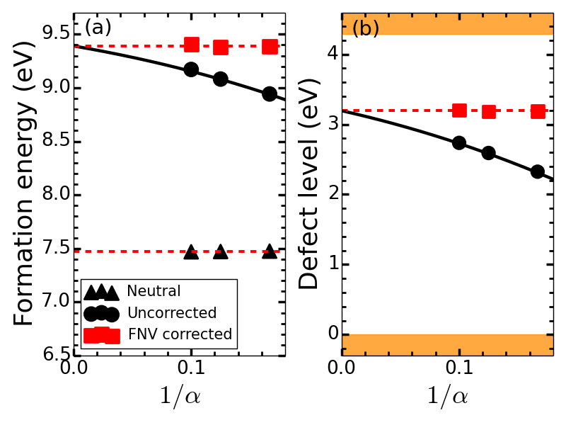
Fig 9 (a) shows the scaling of the uncorrected formation energy of neutral vacancy, , and -1 charged vacancy, , as a function of . The formation energy is computed for nitrogen-rich conditions. The chemical potential for N is taken from N2 molecule. Formation energy of the neutral vacancy is well converged and shows no scaling with the system size. The uncorrected formation energy of the charged vacancy is fit with a polynomial of the form: . and are found to be 9.39, -3.92. The FNV corrected formation energy shows excellent agreement with the extrapolated value for all the super cell sizes considered. Fig 9 (b) shows the dependence of the defect level accomodating the -1 charge with system size. The uncorrected values are fit with a polynomial of the form: . The corrected eigenvalues are in good agreement with the extrapolated value.
4 Workflow
The general
steps involved in computing corrections for the formation energy of
a charged defect are the following (Fig. 10):
-
1.
Compute the total energy of the pristine super cell of the same size. Save the DFT potential in cube/xsf format.
-
2.
Compute the total energy of the super cell (say nnn) containing the neutral defect. Save the DFT potential in cube/xsf format.
-
3.
Compute the total energy of the super cell containing the charged defect. Save the DFT potential in cube/xsf format.
-
4.
Compute term: Compute the model energy for various super cell sizes and extrapolate to obtain . is then given by: (nnn).
-
5.
Compute the potential alignment term , Eqn. 3. The utility script dV_0p.py can be used to compute this.
-
6.
Compute the potential alignment term , Eqn. 6. The utility dV_mD.py can be used to compute this.
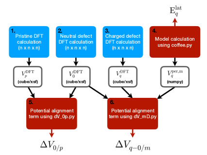
The first three steps are performed by the user with the DFT electronic structure code of his/her choice. The xsf/cube file formats are commonly used to visualize data. Most electronic structure codes provide utilities to convert the DFT potential after a self consistent calculation into these formats. These formats act as an interface between the DFT calculation and the CoFFEE code. The CoFFEE code aids in computing steps 4, 5 and 6. The model calculations are performed by solving the Poisson equation, as detailed above. Details on preparing the input file and running the CoFFEE code to perform these calculations are provided to some extent in the next section and exhaustively in the user guide of the code. The user guide is available for download with the distribution.
5 CoFFEE code framework
5.1 Layout
On unzipping the tar file after download, the CoFFEE folder contains the following directories: PoissonSolver, PotentialAlignment and Examples, and a script coffee.py. The script coffee.py is the main executable. It can be called from the user’s working directory and it performs the model calculation by sequentially calling the relevant functions as depicted in Fig 11. The script coffee.py reads input from a file. The input file contains parameters pertaining to the dimensions of the super cell, the dielectric profile and the model Gaussian charge. The next subsection describes the input file parameters. On running the script, the model total energy is printed out. The model potential, dielectric profile and model charge distribution are written as numpy save files on providing the appropriate flags in the input. The script is run for different supercell sizes and the model energy extrapolated as shown in Fig. 4 (c), 6 (c) and 8 (e) to obtain the isolated model energy.
The PoissonSolver folder holds classes.py which defines three classes: cell, diel_profile and gaussian. Each class has a function to read the parameters pertaining to it from the input file. The cell class has information regarding the cell parameters and the plane wave cut off to be used in the calculation. The diel_profile class has attributes regarding the dielectric profile to be used and functions to construct and Fourier transform the requisite profile. The gaussian class has attributes regarding the construction and Fourier transform of the model gaussian charge. The PoissonSolver folder also consists of three routines, Solver.py, construct_eps.py and PS_main.py. construct_eps.py is used to select and construct the appropriate dielectric profile, based on the user input. Solver.py is used to select the poisson solver to be run. PS_main.py contains the solvers for 1D (PS_1D), 2D (PS_2D) and bulk (PS_3D) systems.

5.2 Input file
The input file is divided into three sections designated with ”&CELL_PARAMETERS”, ”&DIELECTRIC_PARAMETERS” and ”&GAUSSIAN_PARAMETERS”. Each section is ended with a ”/” and contains, in the intervening space, the parameters relevant to the respective section. The following is an example of an input file for in diamond.
&CELL_PARAMETERS # Normalized lattice vectors: a1, a2 and a3 Lattice_Vectors(normalized): 1.000000000 0.000000000 0.000000000 0.000000000 1.000000000 0.000000000 0.000000000 0.000000000 1.000000000 # Cell dimensions. Provide "angstrom" in place # of "bohr" if you wish to specify # these values in angstrom units. # These are multiplied to a1, a2 and a3 respectively. Cell_dimensions bohr 26.594331775231996 26.594331775231996 26.594331775231996 # G-vectors will be used upto this kinetic energy cut off. # Provide "Rydberg" in place of "Hartree" # if you wish to specify the cut off in Rydberg # atomic units. Ecut=20.0 Hartree / # Set "Bulk" here for 3D, bulk systems. &DIELECTRIC_PARAMETERS Bulk # Sets the value of the dielectric constant along a1, a2, a3. Epsilon1_a1 = 5.76 Epsilon1_a2 = 5.76 Epsilon1_a3 = 5.76 / &GAUSSIAN_PARAMETERS: # The charge state of the defect being simulated. Total_charge = -2 # The width of the model Gaussian charge being used. # (default: bohr units) Sigma = 2.614 # These set the center of the Gaussian in crystal # units. Centre_a1 = 0.5 Centre_a2 = 0.5 Centre_a3 = 0.5 /
The default unit of length is bohr, unless ”angstrom” is explicitly specified after the number. Ecut stands for the plane wave energy cut off used in solving the Poisson equation. The string after &DIELECTRIC_PARAMETERS determines the dielectric profile and which Poisson solver is to be called. The dielectric parameters are provided in the input file along the crystal axes. The center of the model charge is specified in crystal units in the &GAUSSIAN_PARAMETERS, along with the charge it carries and the gaussian width. For the nanowire profile, the user can provide a list of points that form the boundary of the cross-section of the wire in a file, based on which the profile is created. The user guide lists all the possible input parameters and the properties they control. Also, the Examples folder has sample profiles for different materials.
5.3 Potential alignment
The PotentialAlignment directory holds two scripts: dV_0p.py and dV_mD.py to compute the two potential alignment terms, and in Eqn. 2 and 4. These scripts read the DFT potential from ”cube” or ”xsf” formats. dV_0p.py plots the planar averaged , in the desired direction. The difference far from the defect can then be read from the plot. This script reads input from a file. The format of the input file:
&dV_0p
file_type = cube # No quotes. Takes cube/xsf
file_neutral = n.cube # No quotes. Path to the neutral DFT potential file
file_pristine = p.cube # No quotes. Path to the pristine DFT potential file
plt_dir = a1 # No quotes. Takes a1/a2/a3. If a1
# is specified, the data is averaged along a2
# and a3 directions and the planar averaged data is plotted
# along a1 in a file pa_dv0p_a1.plot
factor = Ryd # factor to be multiplied to the cube/xsf data. If the data is in
# rydberg and the plot is needed in eV, specify
# factor = Ryd. If the data is in Hartree units,
# specify factor = Hartree
/
dV_mD.py plots the planar averaged and along the desired direction. These can be plotted as shown in Fig. 4 b, 6 b. This script reads input from a file. The format of the input file:
&dV_mD
file_type = cube # No quotes. Format of the DFT potential files: cube/xsf
file_model = m.npy # No quotes. Path to the model potential file (.npy)
file_charged = q.cube # No quotes. Path to the charged DFT potential file
file_neutral = n.cube # No quotes. Path to the neutral DFT potential file
plt_dir = a1 # No quotes. Takes a1/a2/a3. If a1
# is specified, the data is averaged along a2
# and a3 directions and the planar averaged data is plotted
# along a1 in files DFTdiff_a1.plot, model_a1.plot
factor = Ryd # factor to be multiplied to the cube/xsf data. If the data is in
# rydberg and the plot is needed in eV, specify
# factor = Ryd. If the data is in Hartree units,
# specify factor = Hartree
/
5.4 Solver parallelization and optimization
PS_1D, PS_2D and PS_3D are the poisson solver functions in PS_main.py for 1D, 2D and bulk systems. We do not use any parallelization for bulk systems, where the potential is obtained using Eqn 9, since the computation time is fairly small. We have, however, optimized this function with the help of Cython [48]. For 2D systems, linear equations of the form in Eqn 11 are solved. The number of reciprocal lattice vectors depends on the plane wave energy cut off set for the calculation. For and reciprocal lattice vectors along the in-plane reciprocal lattice directions, a set of linear equations are solved. We use the iterative solver bicgstab() which is a part of the SciPy linear algebra package to solve these linear equations. These calculations are computationally intensive for large system sizes. We parallelize the total number of linear equations so that each process solves equations, where is the number of processes. The parallelization is done via MPI, using the package mpi4py [55]. For 1D systems, linear equations are solved as shown in Eqn 14 . These are again parallelized in the package in a similar manner. Furthermore, the efficiency of the bicgstab() routine is primarily determined by the time taken to compute matrix vector products. We optimized these products using Cython [48] to reduce the computation time.
6 Conclusion
We present a complete package, CoFFEE, for electrostatic corrections in charged defect simulations. We demonstrate the application of this code on three test systems, namely: bulk diamond, 2D MoS2 and 1D BN nanoribbon. The corrected formation energy and defect eigenvalues for these systems are found to be in good agreement with the isolated limit extrapolation of the corresponding uncorrected quantities. The code, written completely in Python [47], is parallelized using MPI and the slowest steps accelarated using Cython [48].
7 Acknowledgments
We thank the Supercomputer Education and Research Centre (SERC) at IISc for providing the computational facilities.
References
References
-
[1]
C. Freysoldt, B. Grabowski, T. Hickel, J. Neugebauer, G. Kresse, A. Janotti,
C. G. Van de Walle,
First-principles
calculations for point defects in solids, Rev. Mod. Phys. 86 (2014)
253–305.
doi:10.1103/RevModPhys.86.253.
URL http://link.aps.org/doi/10.1103/RevModPhys.86.253 -
[2]
A. Malashevich, M. Jain, S. G. Louie,
First-principles
study of oxygen vacancies in rutile ,
Phys. Rev. B 89 (2014) 075205.
doi:10.1103/PhysRevB.89.075205.
URL http://link.aps.org/doi/10.1103/PhysRevB.89.075205 -
[3]
M. Jain, J. R. Chelikowsky, S. G. Louie,
Quasiparticle
excitations and charge transition levels of oxygen vacancies in hafnia,
Phys. Rev. Lett. 107 (2011) 216803.
doi:10.1103/PhysRevLett.107.216803.
URL http://link.aps.org/doi/10.1103/PhysRevLett.107.216803 -
[4]
S. Choi, M. Jain, S. G. Louie,
Mechanism for
optical initialization of spin in nv- center in diamond,
Phys. Rev. B 86 (2012) 041202.
doi:10.1103/PhysRevB.86.041202.
URL http://link.aps.org/doi/10.1103/PhysRevB.86.041202 -
[5]
L. Bjaalie, A. Janotti, K. Krishnaswamy, C. G. Van de Walle,
Point defects,
impurities, and small hole polarons in , Phys. Rev. B
93 (2016) 115316.
doi:10.1103/PhysRevB.93.115316.
URL http://link.aps.org/doi/10.1103/PhysRevB.93.115316 -
[6]
I. C. Diallo, D. O. Demchenko,
Native point
defects in gan: A hybrid-functional study, Phys. Rev. Applied 6 (2016)
064002.
doi:10.1103/PhysRevApplied.6.064002.
URL http://link.aps.org/doi/10.1103/PhysRevApplied.6.064002 -
[7]
Y. Kumagai, L. A. Burton, A. Walsh, F. Oba,
Electronic
structure and defect physics of tin sulfides: Sns,
, and ,
Phys. Rev. Applied 6 (2016) 014009.
doi:10.1103/PhysRevApplied.6.014009.
URL http://link.aps.org/doi/10.1103/PhysRevApplied.6.014009 -
[8]
S. R. Lee, A. F. Wright, N. A. Modine, C. C. Battaile, S. M. Foiles, J. C.
Thomas, A. Van der Ven,
First-principles
survey of the structure, formation energies, and transition levels of
as-interstitial defects in ingaas, Phys. Rev. B 92 (2015) 045205.
doi:10.1103/PhysRevB.92.045205.
URL http://link.aps.org/doi/10.1103/PhysRevB.92.045205 -
[9]
V. Wang, Y. Kawazoe, W. T. Geng,
Native point
defects in few-layer phosphorene, Phys. Rev. B 91 (2015) 045433.
doi:10.1103/PhysRevB.91.045433.
URL http://link.aps.org/doi/10.1103/PhysRevB.91.045433 -
[10]
W. Sun, H. Ehteshami, P. A. Korzhavyi,
Structure and
energy of point defects in tic: An ab initio study, Phys. Rev. B 91
(2015) 134111.
doi:10.1103/PhysRevB.91.134111.
URL http://link.aps.org/doi/10.1103/PhysRevB.91.134111 -
[11]
D. Steiauf, J. L. Lyons, A. Janotti, C. G. V. de Walle,
First-principles study of
vacancy-assisted impurity diffusion in zno, APL Materials 2 (9) (2014)
096101.
arXiv:http://dx.doi.org/10.1063/1.4894195, doi:10.1063/1.4894195.
URL http://dx.doi.org/10.1063/1.4894195 -
[12]
C. G. V. de Walle, J. Neugebauer,
First-principles calculations for
defects and impurities: Applications to iii-nitrides, Journal of Applied
Physics 95 (8) (2004) 3851–3879.
arXiv:http://dx.doi.org/10.1063/1.1682673, doi:10.1063/1.1682673.
URL http://dx.doi.org/10.1063/1.1682673 -
[13]
F. de Brito Mota, S. Azevedo, C. M. de Castilho,
Structural
and electronic properties of perfect and defective bn nanoribbons: A dft
study, Physica E: Low-dimensional Systems and Nanostructures 74 (2015) 233
– 240.
doi:http://dx.doi.org/10.1016/j.physe.2015.06.028.
URL http://www.sciencedirect.com/science/article/pii/S1386947715301004 -
[14]
W. Chen, Y. Li, G. Yu, Z. Zhou, Z. Chen,
Electronic structure and
reactivity of boron nitride nanoribbons with stone-wales defects, Journal of
Chemical Theory and Computation 5 (11) (2009) 3088–3095, pMID: 26609988.
arXiv:http://dx.doi.org/10.1021/ct900388x, doi:10.1021/ct900388x.
URL http://dx.doi.org/10.1021/ct900388x -
[15]
A. Manjanath, A. K. Singh,
Low
formation energy and kinetic barrier of stone–wales defect in infinite and
finite silicene, Chemical Physics Letters 592 (2014) 52 – 55.
doi:https://doi.org/10.1016/j.cplett.2013.12.010.
URL http://www.sciencedirect.com/science/article/pii/S0009261413014905 -
[16]
S. Öğüt, J. R. Chelikowsky,
Charge state
dependent jahn-teller distortions of the -center defect in crystalline
si, Phys. Rev. Lett. 91 (2003) 235503.
doi:10.1103/PhysRevLett.91.235503.
URL https://link.aps.org/doi/10.1103/PhysRevLett.91.235503 -
[17]
M. L. Tiago, J. R. Chelikowsky,
Optical
excitations in organic molecules, clusters, and defects studied by
first-principles green’s function methods, Phys. Rev. B 73 (2006) 205334.
doi:10.1103/PhysRevB.73.205334.
URL https://link.aps.org/doi/10.1103/PhysRevB.73.205334 -
[18]
J. Kim, J. W. Wilkins, F. S. Khan, A. Canning,
Extended si
—p[311—p] defects, Phys. Rev. B 55 (1997) 16186–16197.
doi:10.1103/PhysRevB.55.16186.
URL https://link.aps.org/doi/10.1103/PhysRevB.55.16186 -
[19]
H.-P. Komsa, S. Kurasch, O. Lehtinen, U. Kaiser, A. V. Krasheninnikov,
From point to
extended defects in two-dimensional mos2: Evolution of atomic
structure under electron irradiation, Phys. Rev. B 88 (2013) 035301.
doi:10.1103/PhysRevB.88.035301.
URL http://link.aps.org/doi/10.1103/PhysRevB.88.035301 -
[20]
D. Le, T. B. Rawal, T. S. Rahman,
Single-layer mos2 with sulfur
vacancies: Structure and catalytic application, The Journal of Physical
Chemistry C 118 (10) (2014) 5346–5351.
arXiv:http://dx.doi.org/10.1021/jp411256g, doi:10.1021/jp411256g.
URL http://dx.doi.org/10.1021/jp411256g -
[21]
H. L. Tuller, S. R. Bishop,
Point defects
in oxides: Tailoring materials through defect engineering, Annual Review of
Materials Research 41 (1) (2011) 369–398.
arXiv:http://dx.doi.org/10.1146/annurev-matsci-062910-100442, doi:10.1146/annurev-matsci-062910-100442.
URL http://dx.doi.org/10.1146/annurev-matsci-062910-100442 -
[22]
L. Hu, T. Zhu, X. Liu, X. Zhao,
Point defect engineering of
high-performance bismuth-telluride-based thermoelectric materials, Advanced
Functional Materials 24 (33) (2014) 5211–5218.
doi:10.1002/adfm.201400474.
URL http://dx.doi.org/10.1002/adfm.201400474 -
[23]
M. K. Nowotny, L. R. Sheppard, T. Bak, J. Nowotny,
Defect chemistry of titanium
dioxide. application of defect engineering in processing of tio2-based
photocatalysts, The Journal of Physical Chemistry C 112 (14) (2008)
5275–5300.
arXiv:http://dx.doi.org/10.1021/jp077275m, doi:10.1021/jp077275m.
URL http://dx.doi.org/10.1021/jp077275m -
[24]
A. K. Singh, E. S. Penev, B. I. Yakobson,
Vacancy clusters in graphane as
quantum dots, ACS Nano 4 (6) (2010) 3510–3514.
arXiv:http://dx.doi.org/10.1021/nn1006072, doi:10.1021/nn1006072.
URL http://dx.doi.org/10.1021/nn1006072 -
[25]
S. Bhowmick, U. V. Waghmare,
Anisotropy of the
stone-wales defect and warping of graphene nanoribbons: A first-principles
analysis, Phys. Rev. B 81 (2010) 155416.
doi:10.1103/PhysRevB.81.155416.
URL https://link.aps.org/doi/10.1103/PhysRevB.81.155416 -
[26]
C. Freysoldt, J. Neugebauer, C. G. Van de Walle,
Fully
Ab Initio finite-size corrections for charged-defect supercell
calculations, Phys. Rev. Lett. 102 (2009) 016402.
doi:10.1103/PhysRevLett.102.016402.
URL http://link.aps.org/doi/10.1103/PhysRevLett.102.016402 -
[27]
H.-P. Komsa, T. T. Rantala, A. Pasquarello,
Finite-size
supercell correction schemes for charged defect calculations, Phys. Rev. B
86 (2012) 045112.
doi:10.1103/PhysRevB.86.045112.
URL http://link.aps.org/doi/10.1103/PhysRevB.86.045112 -
[28]
Y. Kumagai, F. Oba,
Electrostatics-based
finite-size corrections for first-principles point defect calculations,
Phys. Rev. B 89 (2014) 195205.
doi:10.1103/PhysRevB.89.195205.
URL http://link.aps.org/doi/10.1103/PhysRevB.89.195205 -
[29]
I. Dabo, B. Kozinsky, N. E. Singh-Miller, N. Marzari,
Electrostatics in
periodic boundary conditions and real-space corrections, Phys. Rev. B 77
(2008) 115139.
doi:10.1103/PhysRevB.77.115139.
URL http://link.aps.org/doi/10.1103/PhysRevB.77.115139 -
[30]
M. Leslie, N. J. Gillan,
The energy and elastic
dipole tensor of defects in ionic crystals calculated by the supercell
method, Journal of Physics C: Solid State Physics 18 (5) (1985) 973.
URL http://stacks.iop.org/0022-3719/18/i=5/a=005 -
[31]
N. D. M. Hine, K. Frensch, W. M. C. Foulkes, M. W. Finnis,
Supercell size
scaling of density functional theory formation energies of charged defects,
Phys. Rev. B 79 (2009) 024112.
doi:10.1103/PhysRevB.79.024112.
URL http://link.aps.org/doi/10.1103/PhysRevB.79.024112 -
[32]
W. Chen, A. Pasquarello,
First-principles
determination of defect energy levels through hybrid density functionals and
gw, Journal of Physics: Condensed Matter 27 (13) (2015) 133202.
URL http://stacks.iop.org/0953-8984/27/i=13/a=133202 -
[33]
W. Chen, A. Pasquarello,
Correspondence of
defect energy levels in hybrid density functional theory and many-body
perturbation theory, Phys. Rev. B 88 (2013) 115104.
doi:10.1103/PhysRevB.88.115104.
URL http://link.aps.org/doi/10.1103/PhysRevB.88.115104 -
[34]
G. Makov, M. C. Payne,
Periodic boundary
conditions in ab initio calculations, Phys. Rev. B 51 (1995)
4014–4022.
doi:10.1103/PhysRevB.51.4014.
URL http://link.aps.org/doi/10.1103/PhysRevB.51.4014 -
[35]
S. Lany, A. Zunger,
Assessment of
correction methods for the band-gap problem and for finite-size effects in
supercell defect calculations: Case studies for zno and gaas, Phys. Rev. B
78 (2008) 235104.
doi:10.1103/PhysRevB.78.235104.
URL http://link.aps.org/doi/10.1103/PhysRevB.78.235104 -
[36]
D. Wang, D. Han, X.-B. Li, S.-Y. Xie, N.-K. Chen, W. Q. Tian, D. West, H.-B.
Sun, S. B. Zhang,
Determination
of formation and ionization energies of charged defects in two-dimensional
materials, Phys. Rev. Lett. 114 (2015) 196801.
doi:10.1103/PhysRevLett.114.196801.
URL http://link.aps.org/doi/10.1103/PhysRevLett.114.196801 -
[37]
T.-L. Chan, A. J. Lee, J. R. Chelikowsky,
An
effective capacitance model for computing the electronic properties of
charged defects in crystals, Computer Physics Communications 185 (6) (2014)
1564 – 1569.
doi:https://doi.org/10.1016/j.cpc.2014.02.020.
URL http://www.sciencedirect.com/science/article/pii/S0010465514000642 -
[38]
H.-P. Komsa, A. Pasquarello,
Finite-size
supercell correction for charged defects at surfaces and interfaces, Phys.
Rev. Lett. 110 (2013) 095505.
doi:10.1103/PhysRevLett.110.095505.
URL http://link.aps.org/doi/10.1103/PhysRevLett.110.095505 -
[39]
J.-Y. Noh, H. Kim, Y.-S. Kim,
Stability and
electronic structures of native defects in single-layer
, Phys. Rev. B 89 (2014) 205417.
doi:10.1103/PhysRevB.89.205417.
URL http://link.aps.org/doi/10.1103/PhysRevB.89.205417 -
[40]
H.-P. Komsa, N. Berseneva, A. V. Krasheninnikov, R. M. Nieminen,
Charged point
defects in the flatland: Accurate formation energy calculations in
two-dimensional materials, Phys. Rev. X 4 (2014) 031044.
doi:10.1103/PhysRevX.4.031044.
URL http://link.aps.org/doi/10.1103/PhysRevX.4.031044 -
[41]
H.-P. Komsa, A. V. Krasheninnikov,
Native defects in
bulk and monolayer from first principles, Phys. Rev. B
91 (2015) 125304.
doi:10.1103/PhysRevB.91.125304.
URL http://link.aps.org/doi/10.1103/PhysRevB.91.125304 -
[42]
S. Kim, K. J. Chang, J.-S. Park,
Finite-size
supercell correction scheme for charged defects in one-dimensional systems,
Phys. Rev. B 90 (2014) 085435.
doi:10.1103/PhysRevB.90.085435.
URL http://link.aps.org/doi/10.1103/PhysRevB.90.085435 - [43] D. Vinichenko, M. Gokhan Sensoy, C. M. Friend, E. Kaxiras, Accurate formation energies of charged defects in solids: a systematic approach, ArXiv e-printsarXiv:1701.02521.
-
[44]
M. G. Sensoy, D. Vinichenko, W. Chen, C. M. Friend, E. Kaxiras,
Strain effects on
the behavior of isolated and paired sulfur vacancy defects in monolayer
, Phys. Rev. B 95 (2017) 014106.
doi:10.1103/PhysRevB.95.014106.
URL https://link.aps.org/doi/10.1103/PhysRevB.95.014106 - [45] D. Broberg, B. Medasani, N. Zimmermann, A. Canning, M. Haranczyk, M. Asta, G. Hautier, PyCDT: A Python toolkit for modeling point defects in semiconductors and insulators, ArXiv e-printsarXiv:1611.07481.
-
[46]
E. Péan, J. Vidal, S. Jobic, C. Latouche,
Presentation
of the pydef post-treatment python software to compute publishable charts for
defect energy formation, Chemical Physics Letters 671 (Supplement C) (2017)
124 – 130.
doi:https://doi.org/10.1016/j.cplett.2017.01.001.
URL http://www.sciencedirect.com/science/article/pii/S0009261417300015 - [47] G. Rossum, Python reference manual, Tech. rep., Amsterdam, The Netherlands, The Netherlands (1995).
- [48] S. Behnel, R. Bradshaw, C. Citro, L. Dalcin, D. Seljebotn, K. Smith, Cython: The best of both worlds, Computing in Science Engineering 13 (2) (2011) 31 –39. doi:10.1109/MCSE.2010.118.
-
[49]
X. Gonze, C. Lee,
Dynamical matrices,
born effective charges, dielectric permittivity tensors, and interatomic
force constants from density-functional perturbation theory, Phys. Rev. B 55
(1997) 10355–10368.
doi:10.1103/PhysRevB.55.10355.
URL http://link.aps.org/doi/10.1103/PhysRevB.55.10355 -
[50]
S. Baroni, S. de Gironcoli, A. Dal Corso, P. Giannozzi,
Phonons and related
crystal properties from density-functional perturbation theory, Rev. Mod.
Phys. 73 (2001) 515–562.
doi:10.1103/RevModPhys.73.515.
URL http://link.aps.org/doi/10.1103/RevModPhys.73.515 - [51] P. Giannozzi, S. Baroni, N. Bonini, M. Calandra, R. Car, C. Cavazzoni, D. Ceresoli, G. L. Chiarotti, M. Cococcioni, I. Dabo, A. D. Corso, S. de Gironcoli, S. Fabris, G. Fratesi, R. Gebauer, U. Gerstmann, C. Gougoussis, A. Kokalj, M. Lazzeri, L. Martin-Samos, N. Marzari, F. Mauri, R. Mazzarello, S. Paolini, A. Pasquarello, L. Paulatto, C. Sbraccia, S. Scandolo, G. Sclauzero, A. P. Seitsonen, A. Smogunov, P. Umari, R. M. Wentzcovitch, Quantum espresso: a modular and open-source software project for quantum simulations of materials, Journal of Physics: Condensed Matter 21 (39) (2009) 395502.
- [52] J. P. Perdew, A. tunger, Self-interaction correction to density-functional approximations for many-electron systems, Phys. Rev. B 23 (1981) 5048–5079. doi:10.1103/PhysRevB.23.5048.
-
[53]
P. E. Blöchl,
Projector
augmented-wave method, Phys. Rev. B 50 (1994) 17953–17979.
doi:10.1103/PhysRevB.50.17953.
URL http://link.aps.org/doi/10.1103/PhysRevB.50.17953 - [54] J. P. Perdew, M. Ernzerhof, K. Burke, Rationale for mixing exact exchange with density functional approximations, The Journal of Chemical Physics 105 (22) (1996) 9982–9985. doi:http://dx.doi.org/10.1063/1.472933.
-
[55]
L. Dalcín, R. Paz, M. Storti,
Mpi for python, J.
Parallel Distrib. Comput. 65 (9) (2005) 1108–1115.
doi:10.1016/j.jpdc.2005.03.010.
URL http://dx.doi.org/10.1016/j.jpdc.2005.03.010