MBE growth of 2H-MoTe2 and 1T’-MoTe2 on 3D substrates
Suresh Vishwanath
sv372@cornell.eduSchool of Electrical and Computer Engineering, Cornell University, Ithaca, NY-14853
Department of Electrical Engineering, University of Notre Dame, IN-46556
Aditya Sundar
Department of Materials Science and Engineering, Cornell University, Ithaca, NY-14853
Xinyu Liu
Department of Physics, University of Notre Dame, Notre Dame, IN-46556
Angelica Azcatl
Department of Materials Science and Engineering, University of Texas Dallas, Dallas, TX-75083
Edward Lochocki
Department of Physics, Laboratory of Atomic and Solid State Physics, Cornell University, Ithaca, New York 14853
Arthur R. Woll
Cornell High Energy Synchrotron Source, Cornell University, Ithaca, NY-14853
Sergei Rouvimov
Department of Electrical Engineering, University of Notre Dame, IN-46556
Wan Sik Hwang
Department of Electrical Engineering, University of Notre Dame, IN-46556
Ning Lu
Department of Materials Science and Engineering, University of Texas Dallas, Dallas, TX-75083
Xin Peng
Department of Materials Science and Engineering, University of Texas Dallas, Dallas, TX-75083
Huai-Hsun Lien
Department of Materials Science and Engineering, Cornell University, Ithaca, NY-14853
John Weisenberger
Department of Electrical Engineering, University of Notre Dame, IN-46556
Stephen McDonnell
Department of Materials Science and Engineering, University of Texas Dallas, Dallas, TX-75083
Department of Materials Science and Engineering, University of Virginia, Charlottesville, VA-22904
Moon J. Kim
Department of Materials Science and Engineering, University of Texas Dallas, Dallas, TX-75083
Margaret Dobrowolska
Department of Physics, University of Notre Dame, Notre Dame, IN-46556
Jacek K Furdyna
Department of Physics, University of Notre Dame, Notre Dame, IN-46556
Kyle Shen
Department of Physics, Laboratory of Atomic and Solid State Physics, Cornell University, Ithaca, New York 14853
Kavli Institute at Cornell for Nanoscale Science, Cornell University, Ithaca, New York 14853
Robert M. Wallace
Department of Materials Science and Engineering, University of Texas Dallas, Dallas, TX-75083
Debdeep Jena
School of Electrical and Computer Engineering, Cornell University, Ithaca, NY-14853
Department of Electrical Engineering, University of Notre Dame, IN-46556
Department of Materials Science and Engineering, Cornell University, Ithaca, NY-14853
Huili Grace Xing
grace.xing@cornell.eduSchool of Electrical and Computer Engineering, Cornell University, Ithaca, NY-14853
Department of Electrical Engineering, University of Notre Dame, IN-46556
Department of Materials Science and Engineering, Cornell University, Ithaca, NY-14853
Kavli Institute at Cornell for Nanoscale Science, Cornell University, Ithaca, New York 14853
Abstract
MoTe2 is the least explored material in the Molybdenum-chalcogen family, which crystallizes in thermodynamically stable semiconducting 2H phase at <500C and 1T’ metallic phase at higher temperatures. Molecular beam epitaxy (MBE) provides an unique opportunity to tackle the small electronegativity difference between Mo and Te while growing layer by layer away from thermodynamic equilibrium. For a few-layer MoTe2 grown at a moderate rate of 6 mins per monolayer under varied Te:Mo flux ratio and substrate temperature, the boundary between the 2 phases in MBE grown MoTe2 on CaF2 is characterized using Reflection high-energy electron diffraction (RHEED), Raman spectroscopy and X-ray photoemission spectroscopy (XPS). Grazing incidence X-ray diffraction (GI-XRD) reveals a grain size of 90 Å and presence of twinned grains. XRD, transmission electron miscroscopy, RHEED, low energy electron diffraction along with lack of electrical conductivity modulation by field effect in MBE 2H-MoTe2 on GaAs (111) B show likelihood of excess Te incorporation in the films. Finally, thermal stability and air sensitivity of MBE 2H-MoTe2 is investigated by temperature dependent XRD and XPS, respectively.
Transition metal chalcogenide, MoSe2, MoTe2
I Introduction
MoTe2 is still a relatively unexplored transitional metal dichalcogenide (TMD) and holds great promise. MoTe2 exists in trigonal prismatic (2H structure) semiconducting phase at room temperature and metallic 1T’ phase (monoclinic structure) at high temperatures or metallic Td phase (orthorhombic structure) when metastable 1T’ is cooled to 33C-13CDeng et al. (2016). 1T’ and Td crystal structures have the same in-plane crystal structures but vary in vertical stacking. Monolayer 2H-MoTe2 is predicted to be among the smallest bandgap semiconducting TMDsGong et al. (2013). Using scanning tunneling spectroscopy (STS) measurements, the bandgap of monolayer 2H-MoTe2 has been measured to be between 1.03 eVDiaz et al. (2016) to 1.4 eVChen et al. (2016). 2H-MoTe2 has a close to broken band alignment with materials like SnSe2Schlaf et al. (1999), making them attractive for tunnel based devices such as Esaki diodesYan et al. (2015) and two-dimensional heterojunction interlayer tunneling field effect transistors (Thin-TFETs)Li et al. (2015, 2014). The 1T’ structure is metastable at room temperature when the bulk MoTe2 crystal is quenched rapidly. The Td-MoTe2 is a type II Weyl semimetalDeng et al. (2016), which is a new class of topological material. Traditionally, the transition between 2H and 1T’ phase was thought to be abrupt with respect to temperatureBrewer and Lamoreaux (1990) but recently a mixed phase region has been observed in the phase diagramKeum et al. (2015). The transition between the 2H and 1T’ phase holds promise for applications such as low resistance contactsCho et al. (2015) and phase change memory.
Large area, phase-pure epitaxial growth with layer controllability would enable industrial applications, but growth of MoTe2 is especially challenging, since the electronegativity difference between Mo and Te is just 0.3 eVBernede et al. (2003); Jaegermann and Schmeisser (1986); Gamble (1974), resulting in a weak bond. Until recently, MoTe2 has been obtained using tellurization of e-beam deposited molybdenum or molybdenum oxide filmsZhou et al. (2015); Park et al. (2015); Zhou et al. (2017) or by chemical vapor transport (CVT)Bernede et al. (1996); Keum et al. (2015). In case of tellurizing Mo, 1T’-MoTe2 phase is initially formed at 650C, which can be converted to 2H-MoTe2 by a 3 hour anneal under Te vaporPark et al. (2015). Tellurizing MoO3 transforms to 2H-MoTe2 more readily, but one cannot be sure in achieving 100% percent reduction of oxygen. For CVT grown MoTe2 a mixed phase is observed in the growth temperature range of 500C to 900C based on the tellurium content in MoTexKeum et al. (2015), but under ultrahigh vacuum (UHV) in non-thermodynamic equilibrium conditions, this phase boundary is unknown. For example, the formation of a new metallic nanowire phase has been recently reported upon Te loss by annealing at 400-500C in UHVZhu et al. (2017). We recently demonstrated growth of 2H-MoTe2 using molecular beam epitaxy (MBE) in a superlattice with MoSe2 as well as Bi2Te3Vishwanath et al. (2016), where we used a growth temperature of 380C. Growth temperature of 340CRoy et al. (2016) or 200CDiaz et al. (2016); Chen et al. (2016) have been used in other recent MBE demonstrations of 2H-MoTe2 growth.
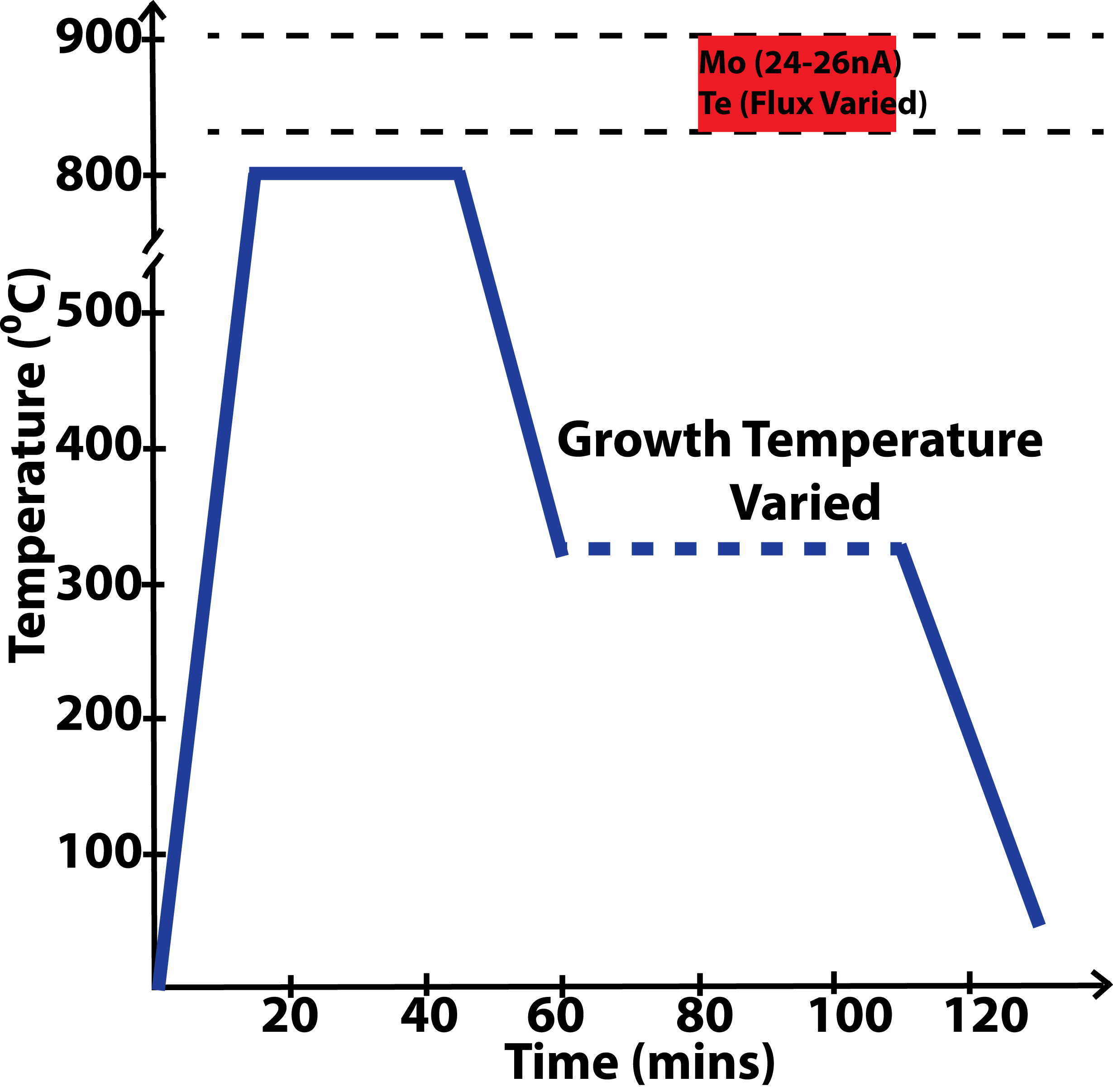
In this study, we chose 340C to be the lower bound of growth temperature, so as to keep the growth temperature higher than the Te cell temperature (300C). This avoids intentional accumulation of Te, while keeping the growth temperature significantly lower than the lower bound (500C) of the mixed phase, as suggested by the phase diagram under 1 ATM of Te vaporKeum et al. (2015). We observe that even at a substrate growth temperature as low as 340C, the crystalline phase of the MBE-grown MoTe2 has a sensitive dependence on Te flux in a Te rich environment. Therefore, in Section A of this paper, we present a series of 3 samples of MoTe2 under different growth conditions and analyze the effect of substrate temperature and tellurium flux on the MoTe2 crystal structure and stoichiometry. Here, we show that it is indeed feasible to grow phase-pure 2H-MoTe2 on a CaF2 substrate without any requirement of a post-growth anneal. In Section B we present the growth and electrical characterization of 2H-MoTe2 on GaAs (111)B. The transition to GaAs was motivated by the availability of high quality epi-ready n GaAs substrates necessary for characterization using techniques such as low energy electron diffraction (LEED). Table.1 summarizes the growth conditions of all the 5 samples in this study. The Mo flux is calculated using the experimentally determined growth rates while assuming zero desorption for molybdenum adatoms, which enables calculation of the Te:Mo flux ratio tabulated in Table.1 for all samples. Growth rate on CaF2 is calculated using cross-section transmission electron microscopy image and on GaAs (111) B from Reflection high-energy electron diffraction (RHEED) oscillations.
Table 1: Growth conditions for all samples in this study
Series
Sample ID
Substrate
MoTe2
Phase
Substrate
Temperature (C)
Te Flux
(Torr)
Te:Mo
flux ratio
Growth
duration
(mins)
Post growth anneal
A
A
CaF2
(111)
2H
340
6.5x10⁻⁶
297
30
none
B
CaF2
(111)
2H+1T’
340
2.0x10⁻⁶
98
30
none
C
CaF2
(111)
1T’
400
1.4x10⁻⁶
71
30
none
B
D
GaAs
(111) B
2H
340
6.9x10⁻⁶
175
30
at 380C for 10 mins
without Te
E
GaAs
(111) B
2H
340
6.9x10⁻⁶
262
20
at 450C for 3 mins and
550C for 7 mins under Te
II Section A : MoTe2 on CaF2
II.1 Growth conditions
Three samples (see Table.1) constitute the series of samples grown on CaF2. Calcium fluoride was chosen as a substrate because (i) it has an inert fluorine-terminated surface on which we have successfully grown MoSe2Vishwanath et al. (2015) and (ii) it provides a cavity effect enhancing the Raman signal due to its optical transparency. On the other hand, the Raman signal from MoTe2 grown on GaAs(111)B is very weakVishwanath et al. (2016). These samples were grown in a Riber 32 MBE system using elemental Mo delivered from an e-beam evaporator and elemental uncracked Te from a Knudsen cell. The growth duration was 30 mins for each sample and the Mo flux, which limits the growth rate, was set to 0.17 monolayer (ML) per minute or 6 minutes per ML. Supplementary (SI) Fig.1 shows that all CaF2 substrates were first heated to 800C, held for 30 mins in order to anneal and degas. Sharp RHEED streaks of CaF2 prior to start of growth (see Fig.1(a)), show the smooth crystalline post-anneal growth surface. Then the substrates were lowered to respective growth temperatures, stabilized for 30 mins prior to thin film growth. The growth conditions are listed in Table.1. Using these 3 samples, we observe that, although the Te flux is 2 orders of magnitude higher than the Mo flux, the Te flux range to obtain 2H-MoTe2 is narrow and the substrate temperature control is critical. None of the MoTe2 films on CaF2 have been annealed in order to avoid phase change during annealing. All temperatures given in this study are thermocouple temperatures and the sample surface temperature is estimated about 20C lower than the thermocouple temperature.
II.2 Results and discussion
II.2.1 Reflection high-energy electron diffraction (RHEED)
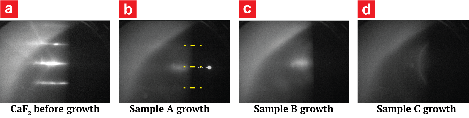
As seen in Fig.1(c), annealed CaF2 has a strong streaky RHEED pattern prior to growth. Sample A shows a more diffused but still streaky RHEED pattern, whereas sample B shows a mixed pattern comprising of streaks and a ring, which evolves into only a ring in sample C. Streaky RHEED points to layered growth with minimal mosaicity of the as-grown film, but progressive inclusion of a ring points to another growth mechanism taking over, which results in polycrystalline growth. Whether the polycrystalline material is the same phase as the streaky film or a different phase is elucidated through employing Raman and XPS characterization (described below). The RHEED streaks of MoTe2 in sample A along <110> appear at the same position as the <10> of CaF2, as observed previously in MoSe2 on CaF2Vishwanath et al. (2015); Koma, Saiki, and Sato (1990). The lattice spacing of MoTe2 based upon the ratio of the RHEED streak spacing is 3.5 Å, which is very close to the value of 3.52 ÅKeum et al. (2015) corresponding to bulk 2H-MoTe2. The ambiguity in this measurement is due to the diffused RHEED pattern, which is measured more accurately using grazing incidence X-ray diffraction (GI-XRD), presented further below.
Figure 1: (a-d)RHEED pattern from the series of samples on CaF2 showing that 1T’ phase grows polycrystalline as compared to well-aligned growth of 2H phase.
II.2.2 Raman Spectroscopy
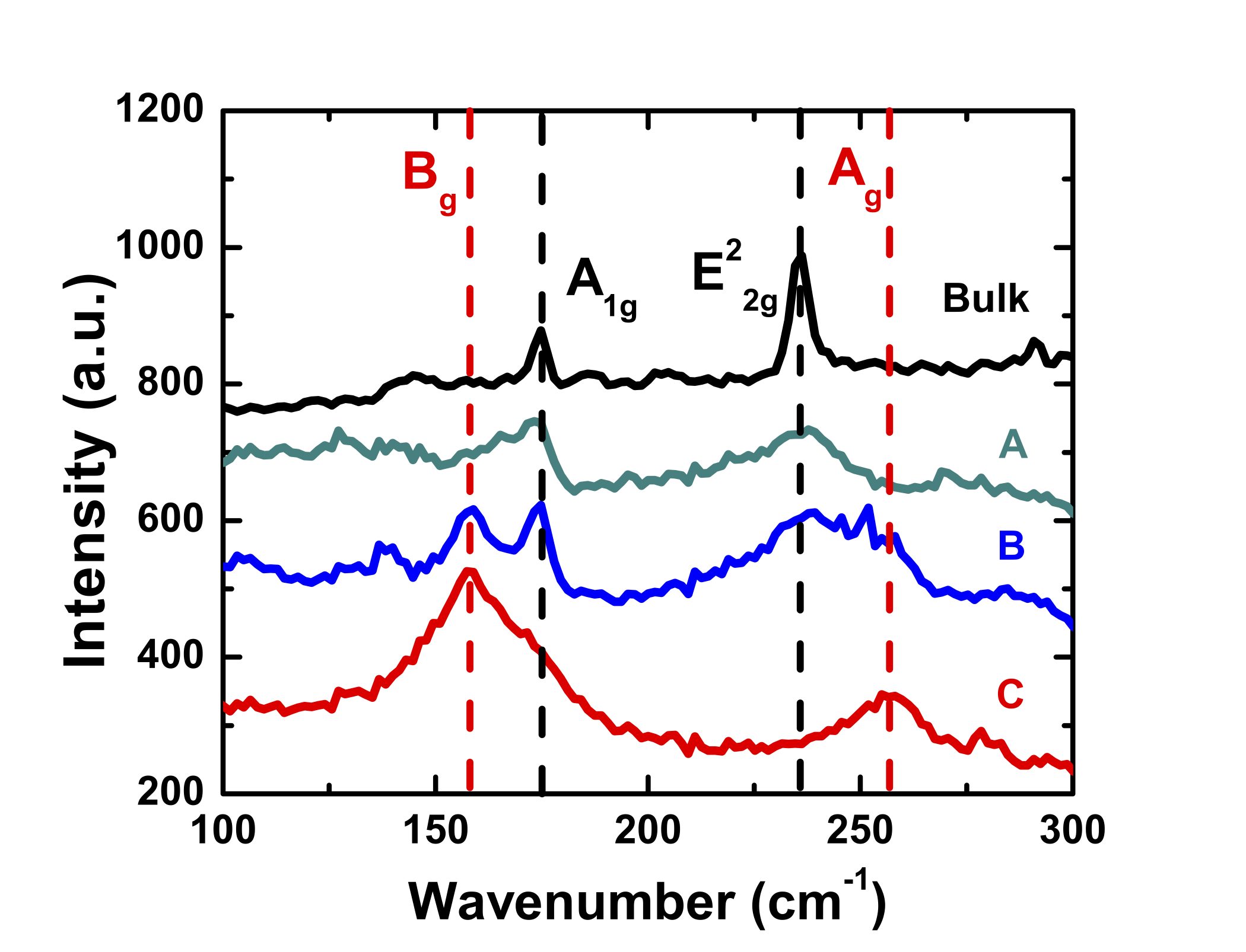
Table 2: Positions of the various Raman peaks compared to measured values for bulk 2H-MoTe2 and reported values for 1T’-MoTe2Park et al. (2015).
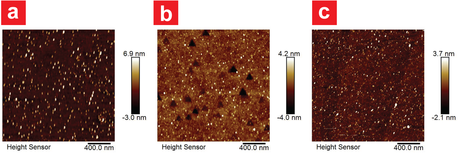
Raman spectra in Fig.2 confirm an evolution from the 2H phase to a new phase as we progress from sample A to sample C. The 2H phase is confirmed by comparing Raman from sample A with Raman from CVT grown bulk 2H-MoTe2 obtained from 2D Semiconductors Inc. as shown in Table.2. Its important to note that the FWHM of the peaks from MBE grown MoTe2 is several times wider than that of the CVT-grown MoTe2. This points to a significant disorder in the MBE-grown material and augments the observation of the diffuse MoTe2 RHEED pattern in sample A. The new phase is assigned to the 1T’ phase due to its proximity to the peak position reported for 1T’ in literaturePark et al. (2015). So far, only 2H and 1T’ or Td phases of MoTe2 are known. As seen in Table.2 the Ag peak position of the 1T’ phase at 255.59 cm-1-256.23 cm-1 agrees closely with the reported value of 256.1 cm-1 - 257 cm-1 for 1T’ MoTe2 growth by tellurization of molybdenum films but the Bg peak at 158.07 cm-1-159.14 cm-1 deviates significantly from the reported value of 163 cm-1 - 161 cm-1 and extremely broadPark et al. (2015)Zhou et al. (2015) . Sample B shows a mixed phase comprised of Raman signatures from both phases, where as sample C only shows 1T’ peaks.
Figure 2: (a) Raman measurements on the samples grown on CaF2.
II.2.3 X-ray photoemission spectroscopy (XPS)
Table 3: XPS peak positions for Mo 3d5/2 and Te 3d5/2 as well as Te:Mo ratio corresponding to both phases 2H-MoTe2 and 1T’-MoTe2 compared to reported values
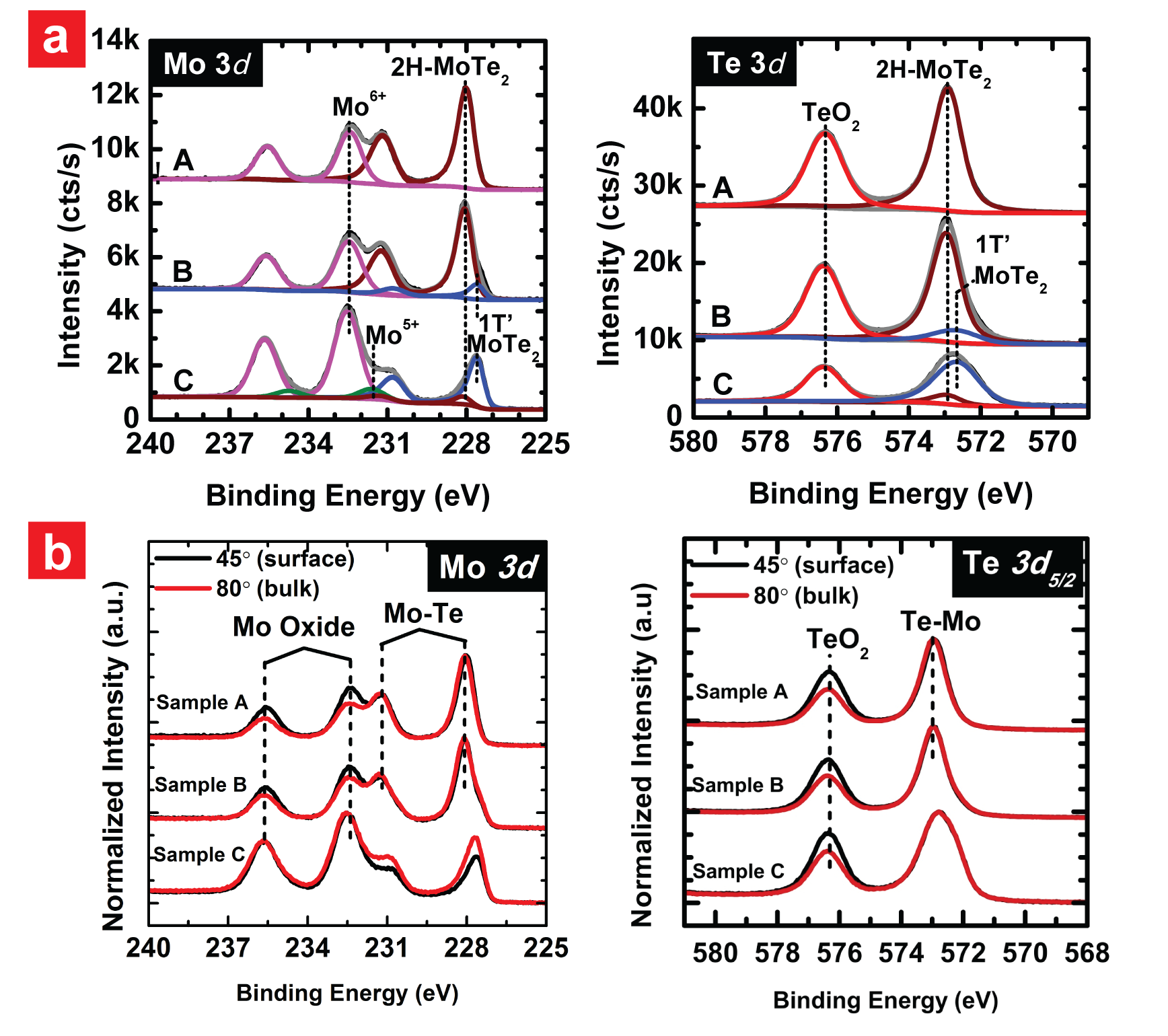
XPS spectra corresponding to Mo, Te, O, Ca, F and C are detected from all samples (Fig.3). No charging effects were detected on any of them. Peak positions for Mo 3d5/2 and Te 3d5/2 as well as Te:Mo ratio corresponding to both phases 2H-MoTe2 and 1T’-MoTe2 are listed in Table.3. For sample A, the Mo 3d5/2 signal corresponding to 2H-MoTe2 bond was detected at 227.9 eV, which is consistent with the binding energy of 2H-MoTe2 in literatureJaegermann and Schmeisser (1986). The Te 3d5/2 peak corresponding to the 2H-MoTe2 is observed at 572.8 eV. Molybdenum oxide in the Mo+6 state was also identified. In the Te 3d spectrum, tellurium dioxide and MoTe2 are both detected. The Te:Mo ratio is 2.57 after correction due to attenuation from the oxide overlayer. For sample B, in addition to the peaks corresponding to 2H-MoTe2, Mo+6 oxide and TeO2 are detected; the Mo 3d5/2 peak at 227.6 eV and the Te 3d5/2 peak at 572.6 eV are assigned to the 1T’ phase. The Te:Mo ratio for the 2H-MoTe2 component is calculated to be 2.03. After correction due to attenuation from the oxide overlayer the Te:Mo ratio is calculated to be 2.54. The Te:Mo ratio for the 1T’-MoTe2 component in sample B is 2.12 and, when corrected for the oxide overlayer is 2.66. For sample C, there is a very small signal from 2H-MoTe2 with Mo 3d5/2 at 228 eV and the corresponding peak for Te 3d5/2 at 572.7 eV. But the majority of the MoTe2 peak intensity is from a new Mo 3d5/2 peak at 227.5 eV and Te 3d5/2 at 572.5 eV, which are assigned to chemical states associated with the 1T’ phase of MoTe2. The Te:Mo ratio corresponding to 1T’ phase of MoTe2 is 2.13 and, when corrected for the oxide overlayer is 2.72. The Te:Mo ratio for the 2H-MoTe2 component is 2.04 and, when corrected for the oxide overlayer, is 2.61. It is key to note that in sample C the Mo 3d peak intensity associated with Mo oxide is much higher than that for MoTe2, as well as the oxide intensity from the other samples. This suggests that, inspite of employing a large over pressure of uncracked Te (dimers) during growth, not only does Mo form predominantly 1T’-MoTe2 but that majority of Mo has an increased propensity for oxidation. This molybdenum oxide in sample C exhibits 2 different Mo oxidation states of +5 and +6. Reported peak position for 1T’-MoTe2 for Mo 3d5/2 is 227.7-228 eV and for Te 3d5/2 is 572.1-572.6 eVNaylor et al. (2016); Zhou et al. (2015). The observed XPS peak from the phase assigned to 1T’-MoTe2 for Te 3d5/2 is consistent with the reported value but that for Mo 3d5/2 is much lower that what has been reported for any Mo-Te bond and even metallic Mo 3d5/2 at 227.8 eVWerfel and Minni (1983). It is also noted that in all 3 samples, the oxide peaks from Mo and Te in the O1s spectra could not be resolved because of the close proximity in electronegativity of Mo and TeBernede et al. (2003). The O 1s spectral feature also has contributions from C-O and O-H. Fig.3(b) shows that concentration of both molybdenum oxide and tellurium oxide concentrations are higher on the surface as seen from the increase in intensity of oxides at take-off angle of 45 as compared to 80. (A take-off angle of 80 is much more bulk sensitive than 45.) Also, the chemical bonding state of MoTe2 is homogeneous through the analyzed depth, as the Mo-Te peak width remains constant when changing angle. Its worthy to note that the extent of oxidation in the telluride system is much more than previously reported MBE MoSe2Vishwanath et al. (2015).
Figure 3: (a) XPS on samples showing various phases and the extent of oxidation under
various growth conditions. The pink line corresponds to Mo+6 oxide, maroon line to 2H-MoTe2, blue line to 1T’-MoTe2, red line to TeO2 and green line to Mo+5 oxide (b) shows that the majority of the oxidation is limited to the surface by comparing the oxide signal from the surface and the bulk by varying the take-off angle.
II.2.4 Grazing incidence X-ray diffraction (GI-XRD) and Transmission electron microscopy (TEM)
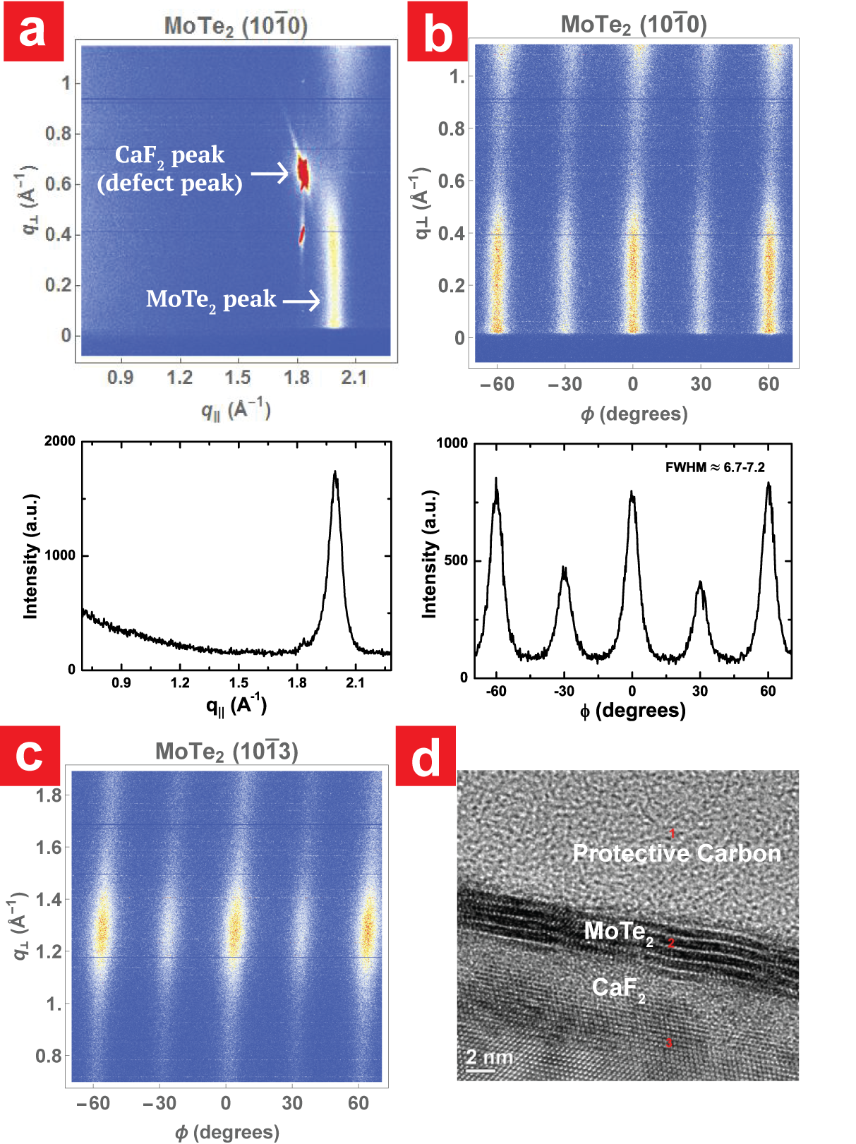
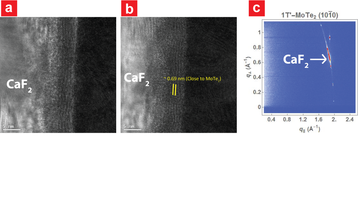
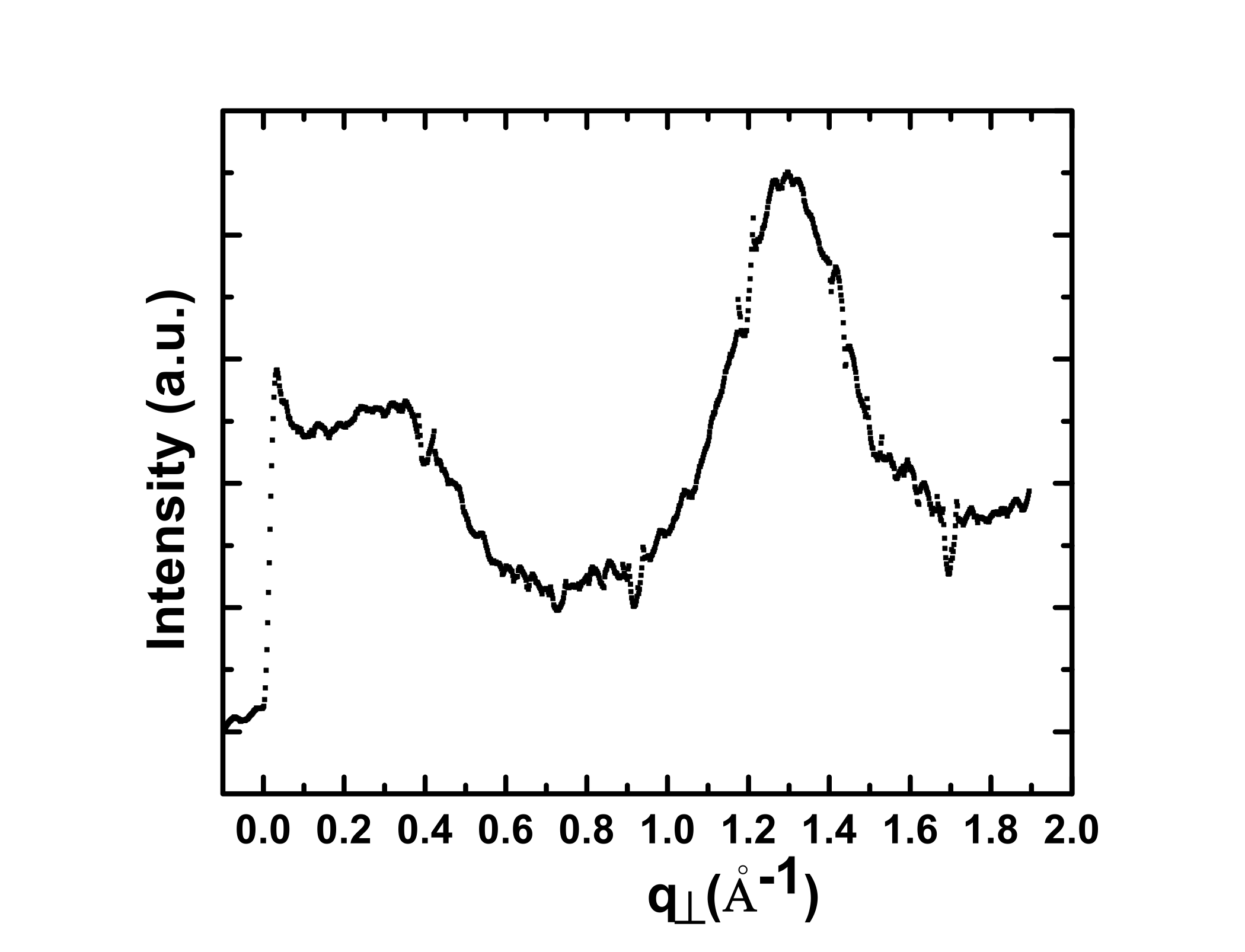
In order to get a better estimation of the inplane lattice constant as compared to the estimation using RHEED pattern, and to understand the preference of in-plane rotational orientation, grazing incidence X-ray diffraction (GI-XRD) was done. GI-XRD from sample A shows (see Fig.4(a)) an extended line corresponding to overlapped 100 and 101 set of planes of MoTe2 and the sharp high intensity peak is from the CaF2 substrate. The in-plane lattice constant of 2H-MoTe2 calculated from the 100 peak corresponds to 3.638 Å. The full width half maximum (FWHM) of 2H-MoTe2 100 peak is calculated to be 0.079 Å-1 and the direct beam FWHM is 0.009 Å-1. By subtracting the width of the direct beam, the genuine FWHM of the 100 peak was estimated to be 0.07 Å-1 which translates to a grain size of 92 ÅShimada et al. (1996). From Fig.4(b), which is an inplane phi() scan, we can see that MBE MoTe2 undergoes significant twinning thus showing 2 sets of 6-fold symmetry diffraction patterns. The peak ratio between adjacent peaks separated by 30 is 0.5. This shows that almost 30% of the grains are twins. Also the wide FWHM (6.7-7.2) of these peaks signifies a large deviation of grains from the preferred orientation. From measurements and simulation it has been shown in 2H-MoSe2 that 101 and 102 peaks are 10 times weaker than 103James and Lavik (1963). 2H-MoTe2 having the same crystal structure as 2H-MoSe2, we also observe the 103 set of peaks at higher q (see Fig.4(c)), from which the out of plane lattice constant (c-spacing) is calculated to be 14.4 Å. The c axis lattice constant obtained from cs-TEM as shown in Fig.4(d) is 13.9 Å. The reported value for the inplane lattice constant and c axis lattice constant from bulk 2H-MoTe2 are 3.52 Å and 13.966 Å, respectively Keum et al. (2015). To understand this discrepancy, we compare the intensity along q (see SI Fig.4) with simulations and observation for various polytypes of NbSe2 by Toshihiro Shimada et al.Shimada et al. (1994) 2H-MoTe2 and 2H-NbSe2 share identical in-plane crystal structures and hence, would give similar intensity profiles along q for various stacking orders (polytypes). Our q (see SI Fig.3) scan closely matches the one reported by Toshihiro Shimada et al.Shimada et al. (1994) on Se-GaAs, which is explained as a combination of 2Hb and 3R NbSe2. 2Hb and 3R both have the trigonal prismatic monolayer but the stacking sequence is different, with 3R having a 3-layer periodicity as compared to 2-layer for 2Hb. The value for MBE 2H-MoTe2 obtained by TEM is spatially local but X-ray beam for GI-XRD has a foot print of 2 mmx10 mm. The excess Te measured using XPS and the presence of stacking faults resulting in mixture of 2Hb and 3R phases could be the reason for the observed larger a and c lattice constants in MBE 2H-MoTe2 compared to bulk 2H-MoTe2.
SI Fig.3(a) shows the cs-TEM of the mixed phase sample B. For 1T’- MoTe2 is known to crystallize in P21/m space group with lattice constants of a=6.33 Å, b=3.48 Å and c=13.82 ÅKeum et al. (2015), where b is very close to the lattice constant of 2H-MoTe2. Therefore, for the sample C since the RHEED shows polycrystalline rings, irrespective of the in-plane rotational orientation of the film, we would expect to observe a ring corresponding to the 010 set of planes in a similar scan as for Sample A (Fig.4(a)). SI Fig.3(c) shows the GI-XRD on sample C ie. 1T’-MoTe2. SI Fig.3(c) shows that there is no signal observed corresponding to 1T’-MoTe2, the only peak is corresponding to CaF2. This is likely due to extremely low signal from the polycrystalline 1T’-MoTe2 thin film. It also shows the variability in crystallinity of CaF2 from substrate to substrate, motivating the use of epi-ready GaAs substrates in Section B.
Figure 4: For sample A (a) in-plane -2 scan showing a peak corresponding to CaF2 and
100 of MoTe2. The extended streak in the perpendicular direction is due to overlap of the extended rods from 100 and 101 in reciprocal space due to the 5 monolayer thin film. Below it is the integrated intensity in a range of 0.02 to 0.15
Å-1 q corresponding to 100 peak(b) The in-plane phi() scan of the 100 peak of MoTe2 to understand the rotational alignment and the extent of twinning in the grown film. Below it is the integrated intensity in a range of 0.02 to 0.15
Å-1 q (c) It shows the periodicity of 103 peak. (d) cs-TEM.
II.2.5 Electrical measurements
Sheet resistivity of the sample A and sample C were measured to be 5468 / and 13255 /, respectively. This is of interest because film on sample A is 2H-MoTe2 and film on sample C is assigned to 1T’-MoTe2. Traditionally 1T’-MoTe2 should be metallic and have lower resistance than 2H-MoTe2 but here the extensive oxidation of Sample C could be the cause of the significant increase in resistivity. TeO2 glasses show semiconducting behaviorHampton et al. (1987).
III Section B : MoTe2 on GaAs (111)B
In this section, 2 samples (sample D and sample E) of MoTe2 on GaAs (111)B are discussed. post-growth anneal was done on MoTe2 films on GaAs.
III.1 Growth conditions for sample D
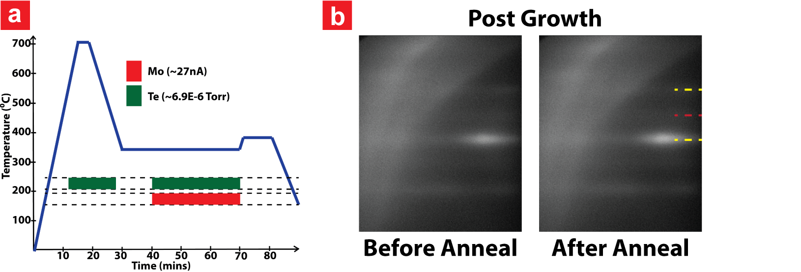
Sample D was grown at a growth temperature of 340C and Te flux of 6.9x10⁻⁶ Torr (slightly higher than Sample A due to higher thermal conductivity of GaAs than CaF2). SI Fig.5(a), shows the growth sequence. The key step in this growth is the anneal of GaAs under Te prior to MoTe2 growth to achieve smoother Te terminated surface. This is consistent with our previous report of Te anneal of GaAsVishwanath et al. (2016) prior to TMD superlattice growth. The change in growth rate between samples (see Table.1) is due to variability of Mo flux at the same e-beam power.
III.2 Results and Discussion
III.2.1 RHEED
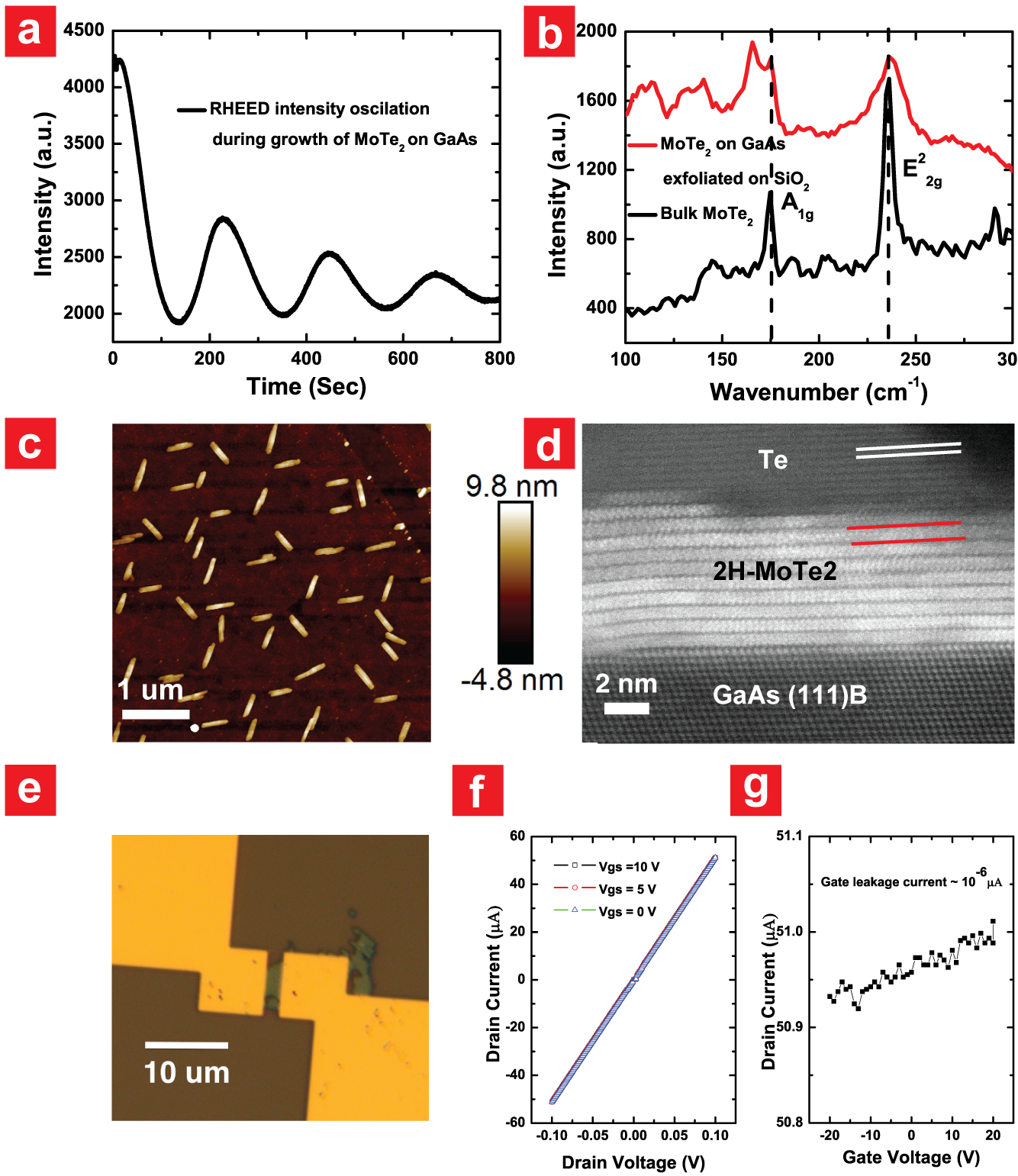
For sample D, a pair of faint RHEED streaks with a spacing less than MoTe2 were observed. Te has a hexagonal crystal structure with lattice constants of a=4.456 Å and c=5.921 ÅAdenis, Langer, and Lindqvist (1989). Since the inplane lattice constant of Te is greater than that of 2H-MoTe2, it was the initial suspect. With the aim to remove any excess Te in the film, a post-growth anneal at 380C without any Te flux was done. But, as seen in SI Fig.5(b), the anneal doesn’t remove this second set of streaks. Further analysis reveals that the ratio of spacing of the RHEED streaks from MoTe2 and the newly observed streaks is 2. If the lines were from MoTe2 and Te, the expected ratio is 1.2. So, its likely not due to elemental tellurium at the surface. One hypothesis is presence of ordered defects, which could be Te interstitials. Fig.5(a) shows RHEED intensity oscillations of the RHEED spectral point during the growth of MBE 2H-MoTe2. This shows close to layer by layer growth. Simulation in SI Fig.7 shows the crest and the trough do not necessarily indicate a complete monolayer, variation in smoothness can cause shifts. But approximately, the period between crests corresponds to a monolayer. Increasing roughness or waviness in the film is the likely cause for decay with RHEED oscillation intensity in Fig.5(a).
III.2.2 Surface morphology, XRD and TEM
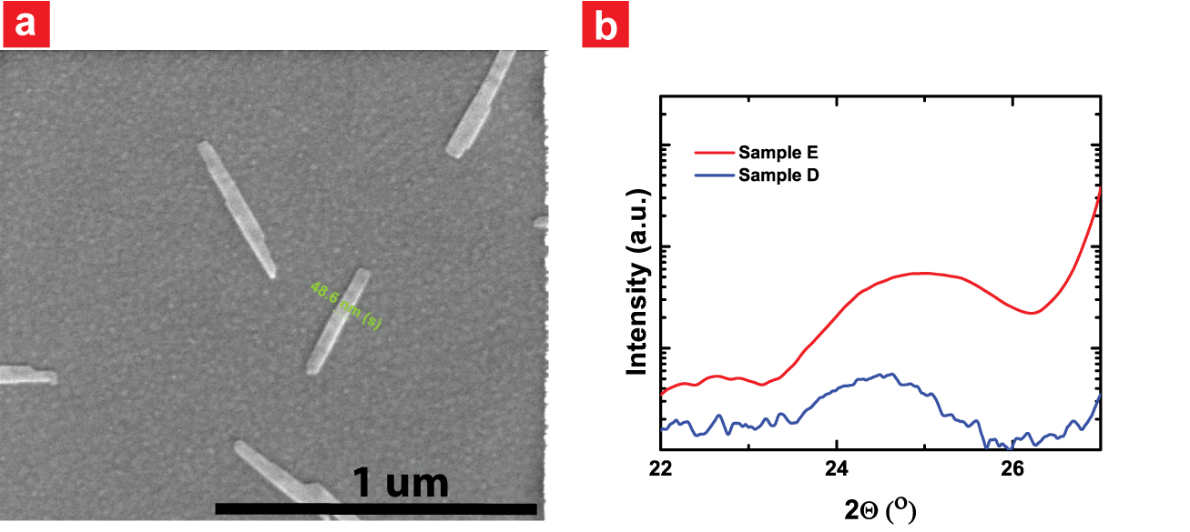
It is very interesting to note that after cooling to room temperature, sample D shows Te crystallites on the surface. From AFM image (Fig.5(c)) and SEM image (SI Fig.6(a)) we can observe that these crystallites have preferential crystallographic orientation with the underlying GaAs (111) with triangular symmetry. Also, we find that the height of these crystallites is 9 nm and about 50 nm wide. The fact that these crystallites are purely tellurium is confirmed by the markedly distinct lattice spacing compared to MoTe2 as seen in the high resolution transmission electron microscopy (HRTEM) image shown in Fig.5(d). This is further confirmed by TEM Energy-dispersive X-ray spectroscopy (not shown). The HRTEM image (Fig.5(d)) also shows a high quality of MoTe2 with a c-axis lattice spacing of 13.9 Å consistent with 2H-MoTe2. These crystallites could have likely been formed during the cooling process to room temperature. We don’t observe Te crystallite formation on films on CaF2 (see SI Fig.2). XRD scan in SI Fig.6((b) shows that at room temperature the (004) peak for sample D appears at 24.46, which is lower than that for bulk 2H-MoTe2 and 1T’-MoTe2Keum et al. (2015). It corresponds to a c-spacing of 14.52 0.05Å. It is analyzed below along with (004) peak of sample E (see Table.4).
III.2.3 Raman and electrical characterization
Since, the Raman signal from MoTe2 on GaAs is quite weakVishwanath et al. (2016), the as grown film was exfoliated and transferred to SiO2/Si substrate using a scotch tape. The transfer was performed to enhance the raman signal from the MoTe2 due to cavity effect from SiO2 as well as to eliminate the interference from the LO phonon raman peaks from GaAs. In Fig.5(b), the peaks below 150 cm-1 can be attributed to TePine and Dresselhaus (1971). E2g peak from transferred MoTe2 from sample D is almost symmetric and peak position is consistent with that from bulk MoTe2 at 235.8 cm-1. The reason for broadening in the A1g peak is unclear. In order to test the electrical characteristic of the transferred MBE grown MoTe2 film, contacts were made to the transferred flake. Using backgating, no modulation was observed (see Fig.5(e and f)).
Figure 5: Sample D: (a) RHEED oscillations at the spectral point during growth of MoTe2 shows a close to layer by layer growth with a period of 218 seconds per monolayer. (b) Raman from MoTe2 grown on GaAs post-exfoliation, using scotch tape, on to SiO2/Si for a better signal. (c) The surface of the thin film post-growth shows several tellurium crystallites, surprisingly with preferential direction of orientation. (d) cross-sectional TEM shows the abrupt interface between GaAs and MoTe2, better quality of 9 monolayer MoTe2 than on CaF2 and pure tellurium crystallite with a significantly different lattice constant and contrast. The pair of white lines and the pair of red lines are a guide to the eye marking the difference in lattice constant of Te and 2H-MoTe2. (e) Optical image of the contacts fabricated to measure transistor characteristics of as grown MoTe2. (f) shows the variation of drain current vs drain voltage at various gate biases and (g) shows that there is no gate modulation and the behavior is similar to a metal.
III.3 Growth conditions for sample E
Sample E was grown on n GaAs for characterizations requiring conducting substrate. Prior to the post-growth anneal, the growth sequence for sample E was identical to sample D. The post-growth anneal for sample E was done at 450C for 3 mins and 550C for 7 mins under Tellurium flux. After this post-growth anneal, the sample was cooled under Te till growth temperature of 340C and then capped with 100 nm Se during cool-down to room temperature for surface protection during sample transfer to other characterization tools.
III.4 Results and Discussion
III.4.1 LEED and XRD data
From the phase diagramBrewer and Lamoreaux (1990), one might expect mixed phase formation during the post-growth anneal at 550C under Te. LEED and XRD was done to check the phase of the film grown. Prior to LEED, the Se cap was desorbed by annealing the sample in UHV at 300C for 30 minutes. A LEED pattern measured with 40 eV electrons (Fig.6(b) shows two sets of spots with the outer hexagonal pattern corresponding to the lattice constant of 2H-MoTe2 (‘a’ lattice constant using LEED = 3.57 0.03 Å)and the inner pattern corresponding to an effective 2x2 superstructure. This is very interesting because it is consistent with the second set of RHEED streaks seen for sample D in SI Fig.5(b), discussed previously. One possible explanation for the extra spots is a change in the surface periodicity relative to the bulk 2H-MoTe2 crystal structure due to a reconstruction or the presence of ordered defects. An alternate possibility is that the large electron spot size (1 mm) may be averaging over three domains of 1T’-MoTe2 rotated by 60 degrees and 120 degrees (See SI Fig.8).
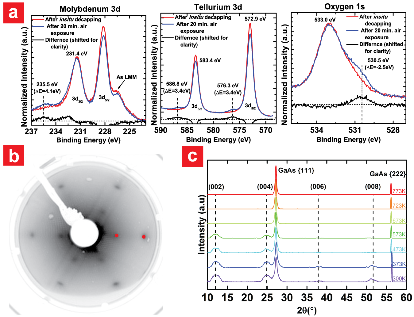
To distinguish between these possibilities, temperature dependent XRD was done on sample E. At room temperature (002), (004), (006) and (008) peak 2 positions of the as grown film are 12.17, 25.02, 38.02 and 51.38 respectively. The reported room temperature 2 positions for the (002), (004), (006) and (008) peaks for 2H-MoTe2 are 12.66, 25.48, 38.63 and 52.34 respectively. D.H Keum et al.Keum et al. (2015) report using temperature dependent XRD that the (004) 2 peak of 2H-MoTe2 is at 25.5 at room temperature and it shifts to slightly greater than 26 at temperatures above 600C corresponding to (004) 2 peak of 1T’-MoTe2. In our case, the (004) 2 peak position is much lower than both peaks (0.5 lower than 2H-MoTe2), which corresponds to a c-spacing of 14.25 0.04Å, and the peaks from the film is lost above 400C. Therefore, without a chalcogen over pressure, MBE grown MoTe2 dissociates between 400C and 500C. Also, sample D (see SI Fig.6(b)) which was grown without anneal at 550C anneal has 0.5 lower than sample E. Peak at smaller 2 implies larger lattice constant but its origin is unclear yet. One possible explanation is the presence of excess tellurium in the crystal, which has been previously reported for bulk crystalsJames and Lavik (1963). The MoTe2 phase diagramBrewer and Lamoreaux (1990) shows that 2H-MoTe2 is not a line compound. The 2H phase of MoTe2 can be formed inspite of a 1% sub- or super- stoichiometric incorporation of tellurium. Hence, as XRD for both samples on GaAs does not show detectable peaks from the 1T’-MoTe2 phase, the 2x2 superstructure observed in LEED, is likely a surface feature rather than the presence of rotated domains of 1T’-MoTe2. Lattice constants obtained from the various techniques described above have been tabulated in Table.4.
Table 4: In-plane and out of plane lattice constants for the 2H-MoTe2 samples in this study obtained by various techniques
To understand the ease of oxidation of MoTe2, on sample E, the Se cap was removed from Sample E by heating in a UHV system, followed by in situ XPS. After the initial XPS measurements, the sample was exposed to air for 20 mins and then XPS done again. It can be clearly seen from Fig.6(a) that oxide peaks appear in both Mo and Te XPS spectrum. Approximately, 8 of the surface area under goes oxidation in 20 mins. Therefore, through the process of exfoliation and fabrication the film is likely to undergo extensive oxidation. For TeO2 glasses the conductivity goes down with lowering temperature but the conduction mechanism is by charge hoppingHampton et al. (1987). The Se decapping is done in an oxide MBE system that is connected to LEED and XPS system to avoid air exposure.The O 1s signal observed in XPS (see Fig.6(a)) prior is air exposure is likely due to physisorbed oxygen, post-decapping, from the oxide MBE chamber (base pressure of 1x10⁻⁸ Torr). This is consistent with the fact that electronegativity difference between Mo and Te is 0.3 eV but that between O and Te is 1.4 eV, making the compound prone to oxidationJaegermann and Schmeisser (1986); Bernede et al. (2003). Effect of air exposure in MBE grown films could be exacerbated by oxidation at the edges of MoTe2 grains, similar to that reported for MBE grown WSe2 filmsPark et al. (2016).
Figure 6: (a) XPS on sample E (MoTe2 on GaAs (111)B) post Se decapping in UHV, prior to and post-air exposure. The dash-dot lines in all 3 spectra show the emergence of the oxide peak (b) LEED from sample E post-decapping without any air exposure, the red spots are guide to the eye demonstrating the 2x2 superstructure (c) Temperature dependent XRD on sample E under nitrogen environment showing the phase of MoTe2 and its thermal stability
IV Conclusion
This work employs extensive large area structural and chemical characterization of MBE grown few layer MoTe2, with complementing electrical characterization. In section A, we show that for growth of few layer 2H-MoTe2 at a low temperature of 340C and growth rate of 6 mins/ML, we need an incident Te:Mo flux greater than 100. The 2H and 1T’ phases formed in different samples have distinct signatures in RHEED, Raman and XPS, but the Te:Mo stoichiometry determined by XPS is greater than 2 for both. GI-XRD shows a small grain size of 90 Å, twinning and a higher-than-expected c-spacing in 2H-MoTe2 on CaF2. XRD on MBE 2H-MoTe2 on GaAs in section B also shows larger c spacing than both bulk 2H-MoTe2 and bulk 1T’-MoTe2. Growth on GaAs shows Te crystallite formation on the surface, and a 2x2 pattern in RHEED and LEED. All these have been hypothesized as signs of excess Te incorporation into 2H-MoTe2 during growth. At ambient pressure in N2 atmosphere, MBE 2H-MoTe2 on GaAs is only stable up to 300C. Excess Te in the film can explain the high electrical conductivity, non-modulating behaviour and easy dissociation of the film with increasing temperature prior to phase transition to the 1T’ phase, a more stable phase at higher temperatures. Finally, we demonstrate the swift oxidation (8 surface area in 20 mins) of the MBE MoTe2 film on exposure to air. With the various complementing large area and local characterizations, this study has provided insight into the few layer MBE growth of Mo-Te system on 3D substrates.
V Experimental Methods
V.0.1 Raman Spectroscopy
Raman measurements were performed in the backscattering configuration using a WITec Alpha 300 system at room temperature. Measurement was done using a 100x objective, 1800 grooves/mm grating, 488 nm laser and 0.75 mW power.
V.0.2 X-ray Photoelectron Spectroscopy
XPS on the CaF2 (Series A) samples was carried out ex-situ using a monochromated Al K source (h = 1486.7 eV) and an Omicron Argus detector (MCD-128) operating with a pass energy of 15 eV. XPS spectra were acquired at a pass energy of 15 eV and take-off angle (defined with respect to the sample surface) of 45 and 80. For XPS peak deconvolution, the spectral analysis software Aanalyzer was employed, where Voigt line shapes and an active Shirley background were used for peak fittingHerrera-Gomez, Hegedus, and Meissner (2002).
XPS on the 2H-MoTe2/nGaAs (Series B) samples was measured using a non-monochromated Al K source and a Scienta R4000 electron analyzer operating at a pass energy of 100 eV. All spectra were measured at normal emission, i.e. 90 degrees relative to the sample surface. Central peak locations were determined by Lorentzian fits with linear backgrounds.
V.0.3 X-ray Diffraction
Out of plane XRD and temperature dependent XRD on the 2H-MoTe2/GaAs samples is done using the Rigaku SmartLab X-Ray Diffractometer with Cu K X-ray source. The GI-XRD is done using the G2 hutch at the CHESS beamline (http://www.chess.cornell.edu/gline/G2.htm), operating with a x-ray energy of 11.31 KeV.
V.0.4 Transmission Electron Microscopy
The atomic structure analysis for sample A and sample D was carried out on FEI Titan 80-300 Transmission Electron Microscope operated at 300 kV.
TEM on sample B was done using JOEL ARM200F atomic resolution analytical microscope.
V.0.5 LEED
LEED on the 2H-MoTe2/nGaAs samples was measured using a Specs ErLEED 3000 system with an incident electron energy of 40 eV. The electron spot size was approximately 1 mm in diameter, and the total angular field of view was 100 degrees. Following the Se decapping at 300C, in situ LEED and XPS measurements were both performed at room temperature in an analysis chamber with pressure below 1x10⁻¹⁰ Torr.
VI Acknowledgments
This work was supported in part by the Center for Low Energy Systems Technology (LEAST), one of six centers of STARnet, a Semiconductor Research Corporation program sponsored by MARCO and DARPA. This work made use of the Cornell Center for Materials Research Shared Facilities which are supported through the NSF MRSEC program (DMR-1120296). This work is based upon research conducted at the Cornell High Energy Synchrotron Source (CHESS) which is supported by the National Science Foundation and the National Institutes of Health/National Institute of General Medical Sciences under NSF award DMR-1332208. MBE growth is in part supported by NSF Grant DMR 1400432 and NSF-EFRI 2DARE Grant DMR 1433490.
VII Supplementary Information
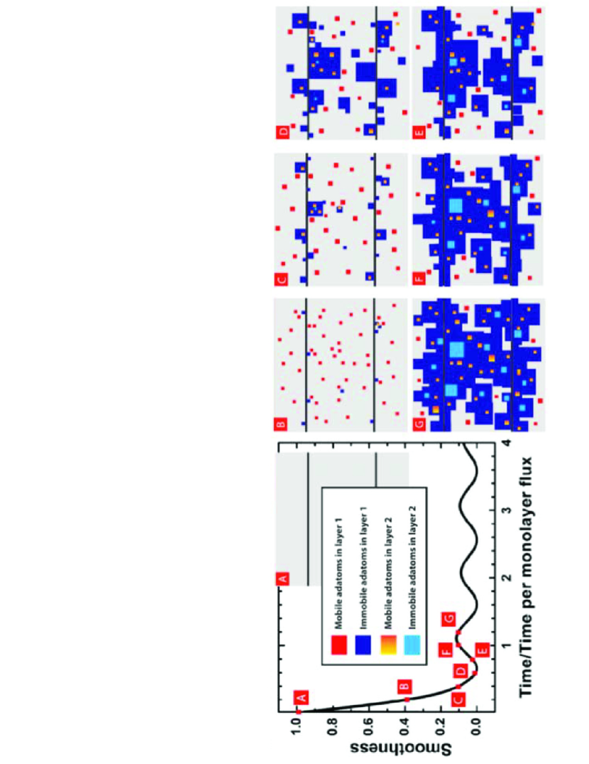
Figure 7: General schematic of the growth diagram of MoTe2 thin film on CaF2.Figure 8: AFM of (a) sample A, (b) sample B and (c) sample C.Figure 9: (a and b)cs-HRTEM of sample B that is the mixed phase MoTe2 and (c) GI-XRD from Sample C that is 1T’ MoTe2. Only signal from CaF2 is observed, none from MoTe2 thin film.Figure 10: Bragg rod profile for 10x peaks from 2H-MoTe2 /CaF2Figure 11: (a) Growth sequence for Sample D and RHEED of MoTe2 on GaAs post growth, (b) pre anneal and (b) post anneal. The dashed lines are guide to the eye, yellow for MoTe2 and red for the additional set of lines observed Figure 12: (a) SEM of sample D showing electrically isolated Tellurium crystallites and (b) the zoom in of the (004) XRD peak from sample D and sample E at room temperature.Figure 13: Simulation of non-equilibrium surface morphology evolution following the subsection 6.3.3 of the book titled “Materials Fundamentals of Molecular Beam Epitaxy” by J.Tsao. RHEED intensity follows closely surface roughness which is a consequence of different number of layer coverage spacially. The 2 black lines corresponds to atomic steps on the substrate where nucleation could occur. In this simulation all kinetic parameters are taken to be 20/time per monolayer flux, expect for the kinetic rate constant for attachment of adatoms to the lower step edge (“down” step), which is slightly higher at 30/time per monolayer flux.
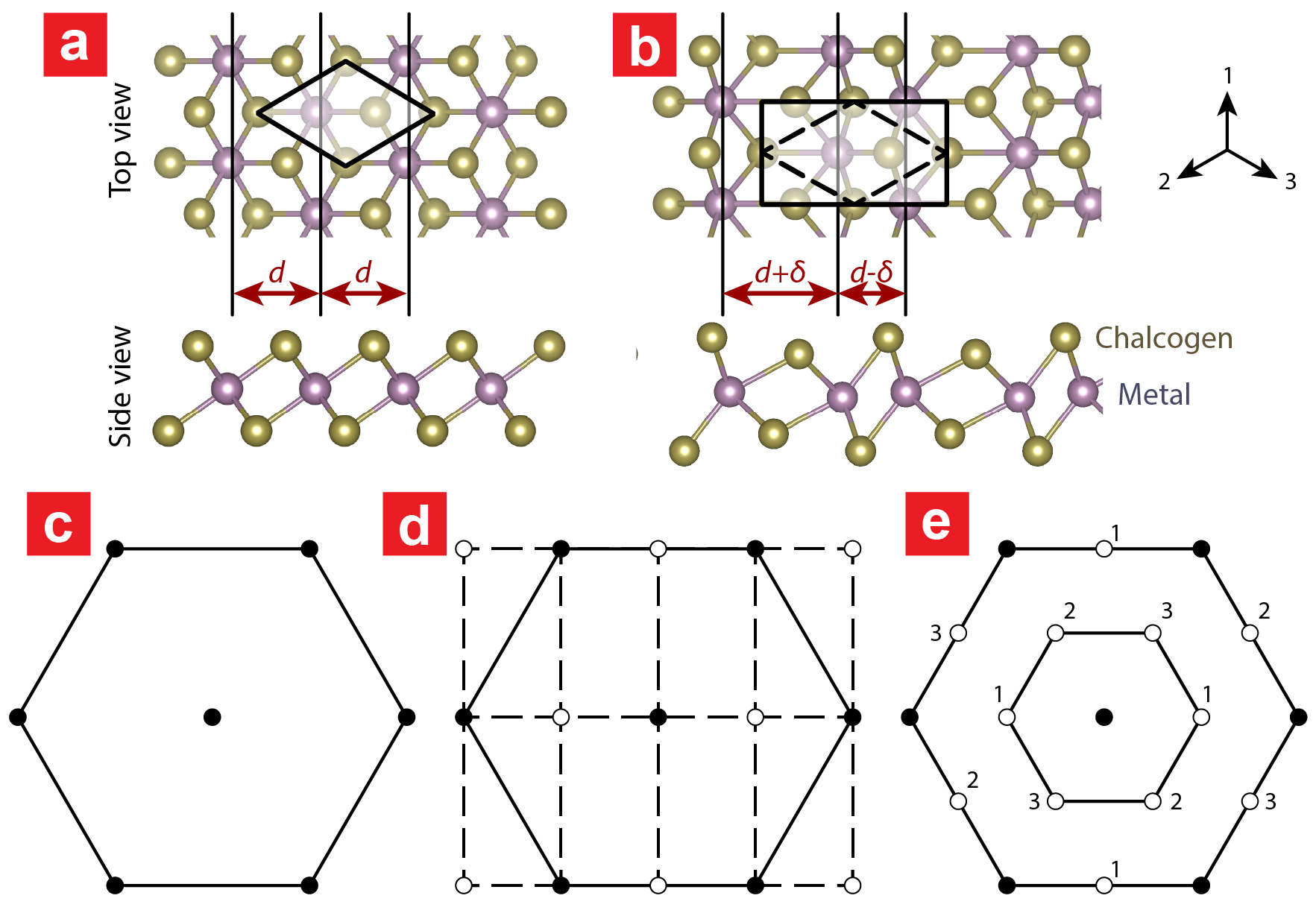
VII.0.1 Possible origins of extra spots in low energy electron diffraction (LEED) patterns from bulk MoTe2
Fig. 8a shows the crystal structure of a monolayer transition metal dichalcogenide with undistorted octahedral transition metal coordination. Lines of metal atoms run in three different directions (referred to as 1, 2, and 3; see inset of Fig. 8b), where each line is separated by a distance d. In the distorted structure, shown in Fig. 8b, the metal atoms shift, creating zigzag chains of metal atoms where two neighboring lines are separated by a smaller distance d-. These chains run along a single direction (in this case, direction 1), causing the unit cell to change from hexagonal to rectangular symmetry. In reciprocal space, extra Bragg reflections appear corresponding to the change in symmetry (Fig. 8c and 8d). Zigzag chains along directions 1, 2, and 3 are degenerate in energy, so it is reasonable to expect domains of different orientation in a macroscopic material. In this case, if the domain size is smaller than the electron beam, a LEED experiment will measure spatially averaged patterns from all three directions (Fig. 8e). The resulting Bragg reflections are identical to those caused by a 2x2 superstructure of the original undistorted crystal.
Bulk 1T’-MoTe2 is formed by stacking individual monolayers with distorted octahedral Mo coordination. At a given incident electron energy, the out-of-plane periodicity determines the intensity of LEED spots but not the position of Bragg reflections. So a bulk 1T’-MoTe2 sample with multiple domains would produce Bragg reflections as shown in Fig. 8e. Alternatively, a bulk 2H-MoTe2 sample would produce Bragg reflections as shown in Fig. 8c. (The 2H structure has trigonal Mo coordination, but retains the same hexagonal symmetry assumed for Fig. 8c.) If the sample surface acquired a larger 2x2 periodicity through a surface reconstruction or the ordering of surface defects, the surface sensitivity of LEED would ensure that the resulting Bragg reflections would appear as in Fig. 8e. Because 2H-MoTe2 and the distorted octahedral structures exhibit the same in-plane lattice constant, the Bragg reflections measured by LEED would appear at identical locations to bulk 1T’-MoTe2 with multiple domains.
Figure 14: (a), (b) Schematics showing crystal structures of monolayer transition metal dichalcogenides with undistorted and distorted octahedral transition metal coordination, respectively. (c), (d) Bragg reflections from the structures in (a) and (b), respectively, where filled (open) circles are from undistorted (distorted) structures. (e) Spatially averaged Bragg reflections resulting from distortions along three different directions, where the open circles are labeled according to the direction of the corresponding distortion.
VIII References
References
Deng et al. (2016)K. Deng, G. Wan, P. Deng, K. Zhang, S. Ding, E. Wang, M. Yan, H. Huang, H. Zhang, Z. Xu, J. Denlinger, A. Fedorov,
H. Yang, W. Duan, H. Yao, Y. Wu, S. Fan, H. Zhang, C. Xi, and S. Zhou, “Experimental observation of topological fermi arcs in
type-ii weyl semimetal mote2,” Nature Physics 12, 1105–1111 (2016).
Gong et al. (2013)C. Gong, H. Zhang,
W. Wang, L. Colombo, R. M. Wallace, and K. Cho, “Band alignment of two-dimensional transition metal dichalcogenides:
Application in tunnel field effect transistors,” Applied Physics Letters 103, 053513 (2013).
Diaz et al. (2016)H. C. Diaz, Y. Ma, R. Chaghi, and M. Batzill, “High density of (pseudo) periodic twin-grain boundaries in
molecular beam epitaxy-grown van der waals heterostructure: Mote2/mos2,” Applied Physics
Letters 108, 191606
(2016).
Chen et al. (2016)J. Chen, G. Wang, Y. Tang, J. Xu, X. Dai, J. Jia, W. Ho, and M. Xie, “Growth, stabilization and conversion of
semi-metallic and semiconducting phases of mote2 monolayer by molecular-beam
epitaxy,” arXiv
preprint arXiv:1612.06105 (2016).
Schlaf et al. (1999)R. Schlaf, O. Lang,
C. Pettenkofer, and W. Jaegermann, “Band lineup of layered semiconductor
heterointerfaces prepared by van der waals epitaxy: Charge transfer
correction term for the electron affinity rule,” Journal of applied physics 85, 2732–2753 (1999).
Yan et al. (2015)R. Yan, S. Fathipour,
Y. Han, B. Song, S. Xiao, M. Li, N. Ma, V. Protasenko, D. A. Muller, D. Jena, and H. G. Xing, “Esaki diodes in van der waals heterojunctions with
broken-gap energy band alignment,” Nano letters 15, 5791–5798 (2015).
Li et al. (2015)M. O. Li, D. Esseni, J. J. Nahas, D. Jena, and H. G. Xing, “Two-dimensional heterojunction interlayer tunneling field
effect transistors (thin-tfets),” IEEE Journal of the Electron Devices Society 3, 200–207 (2015).
Li et al. (2014)M. O. Li, D. Esseni, D. Jena, and H. G. Xing, “Lateral transport in two-dimensional heterojunction
interlayer tunneling field effect transistor (thin-tfet),” in Device Research Conference (DRC), 2014 72nd
Annual (IEEE, 2014) pp. 17–18.
Brewer and Lamoreaux (1990)L. Brewer and R. Lamoreaux, “Mo-te
(molybdenum-tellurium),” Binary Alloy Phase Diagrams, Second Edition, Ed. T.B. Massalski,
ASM International, Materials Park, Ohio 3, 2675–2676 (1990).
Keum et al. (2015)D. H. Keum, S. Cho, J. H. Kim, D.-H. Choe, H.-J. Sung, M. Kan, H. Kang, J.-Y. Hwang, S. W. Kim, H. Yang, K. J. Chang, and Y. H. Lee, “Bandgap opening in few-layered monoclinic
mote2,” Nature
Physics 11, 482–486
(2015).
Cho et al. (2015)S. Cho, S. Kim, J. H. Kim, J. Zhao, J. Seok, D. H. Keum, J. Baik, D.-H. Choe,
K. Chang, K. Suenaga, S. W. Kim, Y. H. Lee, and H. Yang, “Phase patterning for ohmic homojunction contact in mote2,” Science 349, 625–628 (2015).
Bernede et al. (2003)J. Bernede, C. Amory,
L. Assmann, and M. Spiesser, “X-ray photoelectron spectroscopy study
of mote 2 single crystals and thin films,” Applied surface science 219, 238–248 (2003).
Jaegermann and Schmeisser (1986)W. Jaegermann and D. Schmeisser, “Reactivity
of layer type transition metal chalcogenides towards oxidation,” Surface science 165, 143–160 (1986).
Gamble (1974)F. Gamble, “Ionicity, atomic
radii, and structure in the layered dichalcogenides of group ivb, vb, and vib
transition metals,” Journal of Solid State Chemistry 9, 358–367 (1974).
Zhou et al. (2015)L. Zhou, K. Xu, A. Zubair, A. D. Liao, W. Fang, F. Ouyang, Y.-H. Lee, K. Ueno, R. Saito,
T. Palacios, J. Kong, and M. S. Dresselhaus, “Large-area synthesis of high-quality uniform
few-layer mote2,” Journal of the American Chemical Society 137, 11892–11895 (2015).
Park et al. (2015)J. C. Park, S. J. Yun,
H. Kim, J.-H. Park, S. H. Chae, S.-J. An, J.-G. Kim, S. M. Kim, K. K. Kim, and Y. H. Lee, “Phase-engineered
synthesis of centimeter-scale 1t′-and 2h-molybdenum ditelluride thin
films,” ACS
nano 9, 6548–6554
(2015).
Zhou et al. (2017)J. Zhou, F. Liu, J. Lin, X. Huang, J. Xia, B. Zhang, Q. Zeng,
H. Wang, C. Zhu, L. Niu, X. Wang, W. Fu, P. Yu, T.-R. Chang, C.-H. Hsu, D. Wu, H.-T. Jeng, Y. Huang, H. Lin, Z. Shen, C. Yang, L. Lu, K. Suenaga, W. Zhou,
S. T. Pantelides,
G. Liu, and Z. Liu, “Large-area and high-quality 2d transition metal
telluride,” Advanced Materials 29, 1603471 (1–8) (2017).
Bernede et al. (1996)J. Bernede, M. Kettaf,
A. Khelil, and M. Spiesser, “p-n junctions in molybdenum ditelluride,” physica status
solidi (a) 157, 205–209
(1996).
Zhu et al. (2017)H. Zhu, Q. Wang, C. Zhang, R. Addou, K. Cho, R. M. Wallace, and M. J. Kim, “New
mo6te6 sub-nanometer-diameter nanowire phase from 2h-mote2,” Advanced Materials (2017).
Vishwanath et al. (2016)S. Vishwanath, X. Liu,
S. Rouvimov, L. Basile, N. Lu, A. Azcatl, K. Magno, R. M. Wallace, M. Kim, J.-C. Idrobo,
J. K. Furdyna, D. Jena, and H. G. Xing, “Controllable growth of layered selenide and telluride
heterostructures and superlattices using molecular beam epitaxy,” Journal of
Materials Research 31, 900–910 (2016).
Roy et al. (2016)A. Roy, H. C. Movva,
B. Satpati, K. Kim, R. Dey, A. Rai, T. Pramanik, S. Guchhait,
E. Tutuc, and S. K. Banerjee, “Structural and electrical properties of
mote2 and mose2 grown by molecular beam epitaxy,” ACS applied materials & interfaces 8, 7396–7402 (2016).
Vishwanath et al. (2015)S. Vishwanath, X. Liu,
S. Rouvimov, P. C. Mende, A. Azcatl, S. McDonnell, R. M. Wallace, R. M. Feenstra, J. K. Furdyna, D. Jena, , and H. G. Xing, “Comprehensive
structural and optical characterization of mbe grown mose2 on graphite, caf2
and graphene,” 2D Materials 2, 024007
(2015).
Koma, Saiki, and Sato (1990)A. Koma, K. Saiki, and Y. Sato, “Heteroepitaxy of a two-dimensional
material on a three-dimensional material,” Applied surface science 41, 451–456 (1990).
Naylor et al. (2016)C. H. Naylor, W. M. Parkin,
J. Ping, Z. Gao, Y. R. Zhou, Y. Kim, F. Streller, R. W. Carpick, A. M. Rappe,
M. Drndic, J. M. Kikkawa, and A. T. C. Johnson, “Monolayer single-crystal 1t′-mote2
grown by chemical vapor deposition exhibits weak antilocalization effect,” Nano letters 16, 4297–4304 (2016).
Werfel and Minni (1983)F. Werfel and E. Minni, “Photoemission study of the
electronic structure of mo and mo oxides,” Journal of Physics C: Solid State Physics 16, 6091 (1983).
Shimada et al. (1996)T. Shimada, H. Nishikawa,
A. Koma, Y. Furukawa, E. Arakawa, K. Takeshita, and T.-i. Matsushita, “Polytypes and crystallinity of ultrathin epitaxial films of layered
materials studied with grazing incidence x-ray diffraction,” Surface science 369, 379–384 (1996).
James and Lavik (1963)P. James and M. Lavik, “The crystal structure of
mose2,” Acta
Crystallographica 16, 1183–1183 (1963).
Shimada et al. (1994)T. Shimada, Y. Furukawa,
E. Arakawa, K. Takeshita, T. Matsushita, H. Yamamoto, and A. Koma, “Structure determination of ultrathin nbse2 films by
grazing incidence x-ray diffraction,” Solid state communications 89, 583–586 (1994).
Hampton et al. (1987)R. Hampton, W. Hong,
G. Saunders, and R. El-Mallawany, “The electrical conductivity
of pure and binary teo2 glasses,” Journal of non-crystalline solids 94, 307–314 (1987).
Adenis, Langer, and Lindqvist (1989)C. Adenis, V. Langer, and O. Lindqvist, “Reinvestigation of the
structure of tellurium,” Acta Crystallographica Section C: Crystal Structure
Communications 45, 941–942 (1989).
Pine and Dresselhaus (1971)A. Pine and G. Dresselhaus, “Raman
spectra and lattice dynamics of tellurium,” Physical Review B 4, 356 (1971).
Park et al. (2016)J. H. Park, S. Vishwanath,
X. Liu, H. Zhou, S. M. Eichfeld, S. K. Fullerton-Shirey, J. A. Robinson, R. M. Feenstra, J. Furdyna, D. Jena, and H. G. Xing, “Scanning tunneling
microscopy and spectroscopy of air exposure effects on molecular beam epitaxy
grown wse2 monolayers and bilayers,” ACS nano 10, 4258–4267 (2016).
Herrera-Gomez, Hegedus, and Meissner (2002)A. Herrera-Gomez, A. Hegedus, and P. Meissner, “Chemical depth
profile of ultrathin nitrided sio 2 films,” Applied physics letters 81, 1014–1016 (2002).