Topological Dirac Nodal-net Fermions in AlB2-type TiB2 and ZrB2
Abstract
Based on first-principles calculations and effective model analysis, a Dirac nodal-net semimetal state is recognized in AlB2-type TiB2 and ZrB2 when spin-orbit coupling (SOC) is ignored. Taking TiB2 as an example, there are several topological excitations in this nodal-net structure including triple point, nexus, and nodal link, which are protected by coexistence of spatial-inversion symmetry and time reversal symmetry. This nodal-net state is remarkably different from that of IrF4, which requires sublattice chiral symmetry. In addition, linearly and quadratically dispersed two-dimensional surface Dirac points are identified as having emerged on the B-terminated and Ti-terminated (001) surfaces of TiB2 respectively, which are analogous to those of monolayer and bilayer graphene.
I Introduction
In the band theory of solids, a nodal point is a point of contact between conduction and valence bands. One way to classify nodal points is based on their dimensionality Chiu et al. (2016); Bzdušek et al. (2016); Kobayashi et al. (2017); Burkov et al. (2011), which can be divided into three categories. The first is zero-dimensional (0D) nodal points including Weyl points Wan et al. (2011); Weng et al. (2015a); Huang et al. (2015a); Xu et al. (2015); Lv et al. (2015); Soluyanov et al. (2015), Dirac points Novoselov et al. (2005); Wang et al. (2012); Liu et al. (2014); Young et al. (2012), triple points Zhu et al. (2016); Weng et al. (2016); Chang et al. (2016), and other higher degeneracy nodal points Bradlyn et al. (2016). The second is one-dimensional (1D) nodal line systems which include nodal ring Hu et al. (2016); Bian et al. (2016), nodal chain Bzdušek et al. (2016); Yu et al. (2017a) and nodal net Bzdušek et al. (2016). The third is two-dimensional (2D) nodal surfaces Liang et al. (2016). A semimetal with such nodal points is called a topological semimetal (TS), such as Weyl semimetal (WSM), Dirac semimetal (DSM), Dirac nodal line semimetal (DNLSM), nodal chain semimetal, et al.
The 0D nodal point system has been extensively studied during the past decade, due to its non-trivial topological properties and its exotic transport properties. For example, Dirac semimetal has been predicted to be a good candidate for quantum devices because of its massless Dirac fermion’s properties Novoselov et al. (2005); Zhang et al. (2005); Wang et al. (2012); Liu et al. (2014), Weyl semimetals have chiral anomaly which leads to a chiral magnetic effect Son and Yamamoto (2012); Song et al. (2016) i.e. an electric current parallel to an external magnetic field Vazifeh and Franz (2013); Fukushima et al. (2008); Ali et al. (2014); Zyuzin and Burkov (2012); Hosur and Qi (2013); Huang et al. (2015b), and a triple point metal could have topological Lifshitz transitions Zhu et al. (2016).
Investigations of 1D nodal line systems have been developing recent years, due to their great potential in diverse developments in materials science. A nodal line system has a non-trivial Berry phase around the nodal line which would shift the Landau level index by 1/2 Carmier and Ullmo (2008); Yan et al. (2017), and leads to drumhead surface states (SSs) Fang et al. (2016); Yu et al. (2017b). There are many types of nodal line systems, such as single and multiple Dirac nodal line (DNL) systems in the absence of spin-orbit coupling (SOC) Burkov et al. (2011); Bian et al. (2016); Hirayama et al. (2017); Cheng et al. (2017); Liang et al. (2016); Kim et al. (2015); Fang et al. (2015), nexus Heikkila and Volovik (2015); Hyart and Heikkila (2016); Zhu et al. (2016), nodal chain with SOC Bzdušek et al. (2016), and other crossing nodal lines Yu et al. (2017a); Weng et al. (2015b); Kim et al. (2015); Yu et al. (2015); Yan et al. (2017); Chang and Yee (2017); Chen et al. (2017); Kobayashi et al. (2017). All the proposed nodal line systems are protected by crystallographic symmetry. Some are protected by the coexistence of time-reversal symmetry and spatial-inversion symmetry , namely symmetry Cheng et al. (2017); Bian et al. (2016); Liang et al. (2016); Kim et al. (2015). Some are protected by mirror symmetry or glide symmetry Chiu and Schnyder (2014); Bzdušek et al. (2016).
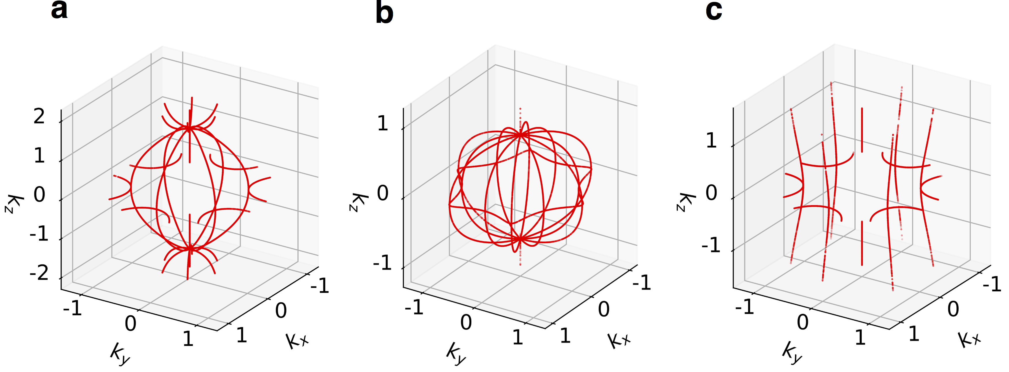
In this work, based on first-principles calculations, we theoretically study a new type of nodal structure, namely nodal net, in two AlB2-type diborides TiB2 and ZrB2, which present a unique combination of properties such as high bond strengths, high melting points, high thermal conductivities, low electrical resistance and low work functions and can be easily synthesized in the laboratory Waśkowska et al. (2011); Okamoto et al. (2010); Kumar et al. (2012); Wang et al. (2011). To better understand this complex nodal net structure, we find it including four classes nodal line structures: A, nodal ring in plane surrounding point; B, nodal line in three vertical mirror planes , and (see definition on p. 273 of Altmann and Herzig (1994)); C, nodal line along starting from a triple point; and D, a single isolated nodal ring at =0.5 plane surrounding point. Furthermore, class-A and class-B nodal lines will cross at a k-point along the direction. All three class-B nodal lines in the vertical mirror planes terminate at point, which is also a termination of the class-C nodal line. So point is also called a neuxs point Cornwall (1999); Heikkila and Volovik (2015), which is the termination of several Dirac line nodes. This nodal net structure differs from previously reported 0D and 1D nodal structures which may lead to some new magnetic and electrical transport properties. In addition, the linearly and quadratically dispersed surface Dirac cones are found at the point of the surface BZ for B-terminated and Ti-terminated surfaces of TiB2 respectively.
This paper is organized as follows. In Section.II, we elucidate the crystal and electronic structure of TiB2. In Section.III, we study the complex nodal net structure both using first-principles calculations and effective model analysis. In Section.IV, we study the drumhead surface states both for B-terminated and Ti-terminated surfaces of TiB2, where a linearly and a quadratically dispersed surface Dirac points are found.
II Crystal and band structure of AlB2-type TiB2
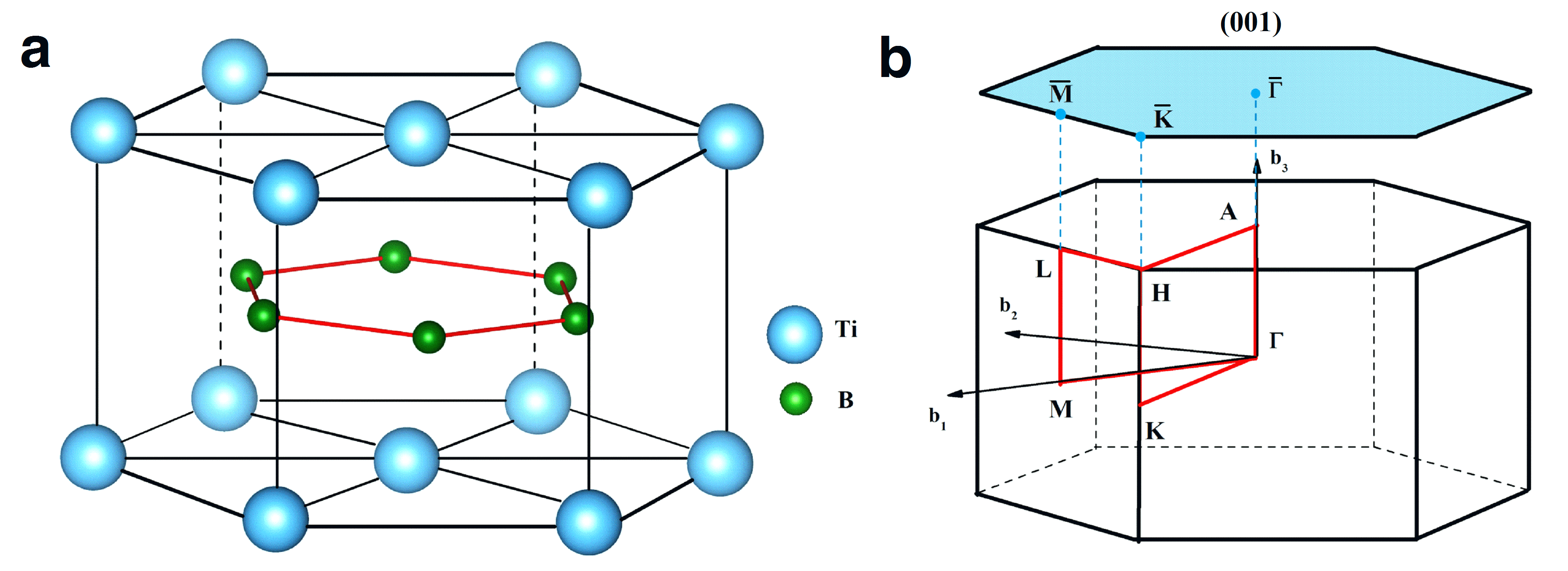
The crystallographic data of TiB2 and ZrB2 are obtained from Ref.Kumar et al. (2012). TiB2 and ZrB2 have the same AlB2-type centro-symmetric crystal structures with the space group P6/mmm (191). As verified by calculation, we find TiB2 (Fig.2) and ZrB2 (Fig 6 in Appendix) have similar electronic structures, therefore, we take TiB2 as an example hereafter. As shown in Fig.1a, it is a layered hexagonal structure with alternating close-packed hexagonal layers of titanium and graphene-like boron layers. The optimized lattice constants are a=b=3.0335 and c=3.2263 , which agree well with the experimental Post et al. (1954) and other theoretical Milman and Warren (2001) results.
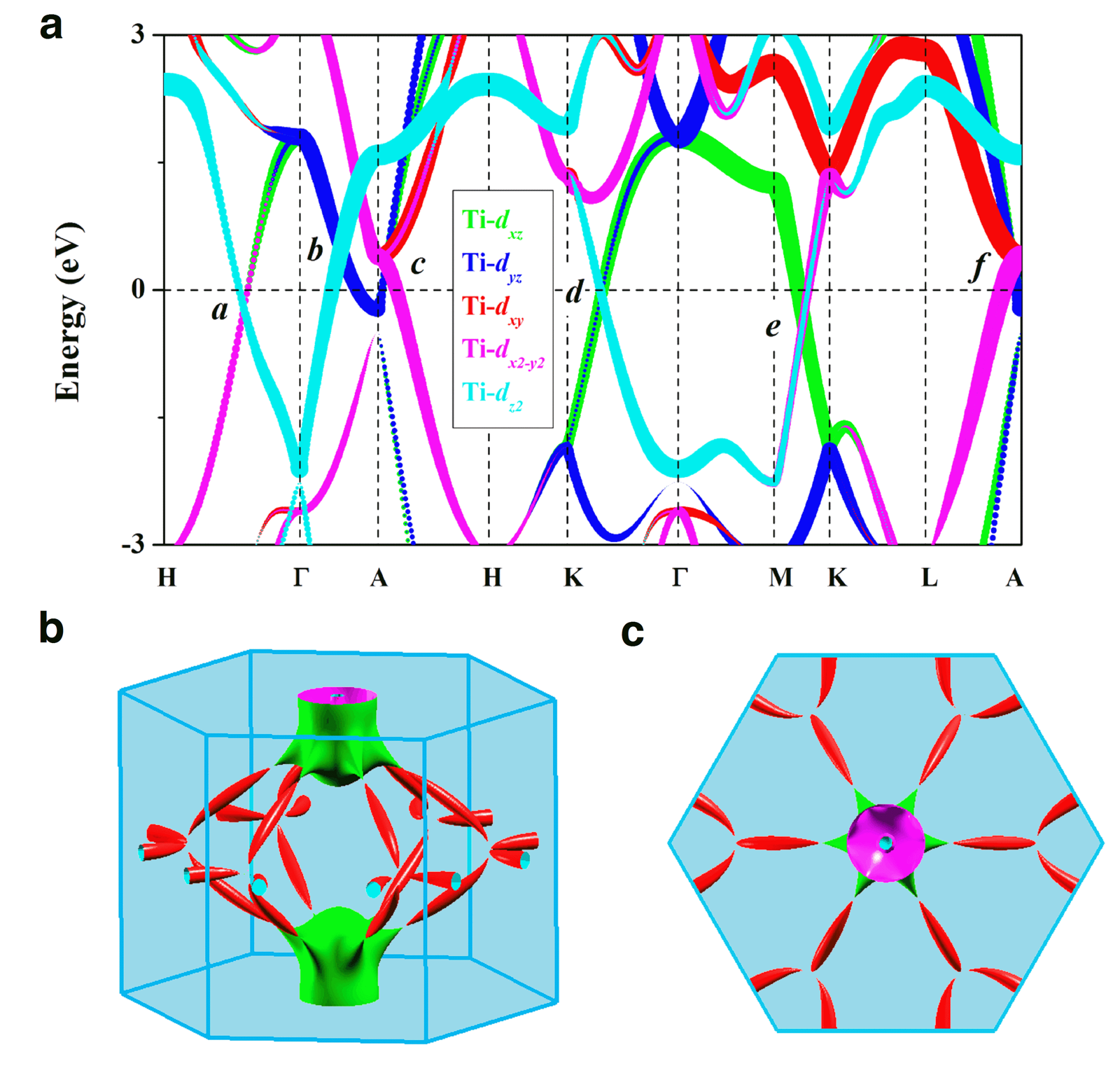
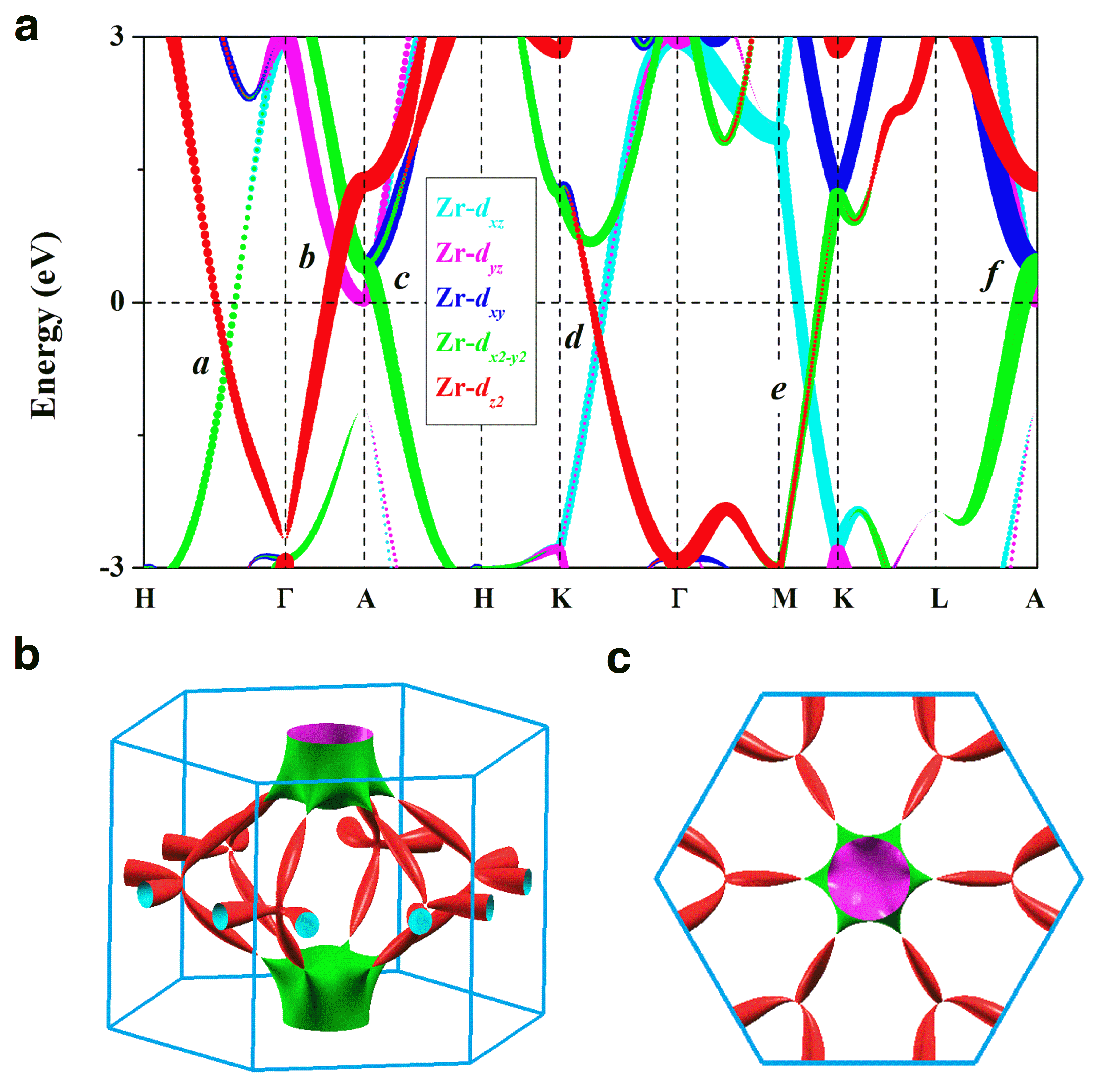
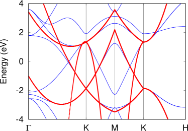
To study the electronic properties of TiB2, the electronic band structure (BS) is calculated in absence of SOC (see details in Appendix A), as shown in Fig.2a. It shows that the valence and conduction bands near the Fermi level exhibit Dirac linear dispersion. There are six band crossing points (also called nodal points (NPs)) located along the H-, -A, A-H, K-, M-K and L-A lines (marked as a to f points in Fig.2a). It is noticed that these six NPs deviate from the Fermi level about -0.16 eV, 0.5 eV, 0.35 eV, -0.01 eV, -0.28 eV and 0.32 eV, respectively. To investigate the formation mechanism of these crossing points, orbital-character analysis is performed. As shown in Fig.2a, the Ti 4d states in TiB2 are dominant feature for these six NPs. Specifically, a is dominated by Ti-dxz, Ti-dx2-y2, and Ti-dz2 orbitals; b is dominated by Ti-dyz and Ti-dz2 orbitals; c is dominated by Ti-dxy, Ti-dyz and Ti-dx2-y2 orbitals; d is dominated by Ti-dxz and Ti-dz2 orbitals; e is dominated by Ti-dxz, Ti-dx2-y2 and Ti-dz2 orbitals, and f is dominated by Ti-dyz and Ti-dx2-y2 orbitals, respectively. The Fermi surface (FS) of TiB2 is calculated and shown in Fig. 2b and 2c, which shows a lantern-like frame with compensated electron pockets and hole pockets, which is a feature of a topological semimetal and also will lead to non-saturated large positive magnetoresistance Ali et al. (2014). The FS calculated in this work agrees well with previous experimental Tanaka and Ishizawa (1980) and theoretical studies Kumar et al. (2012).
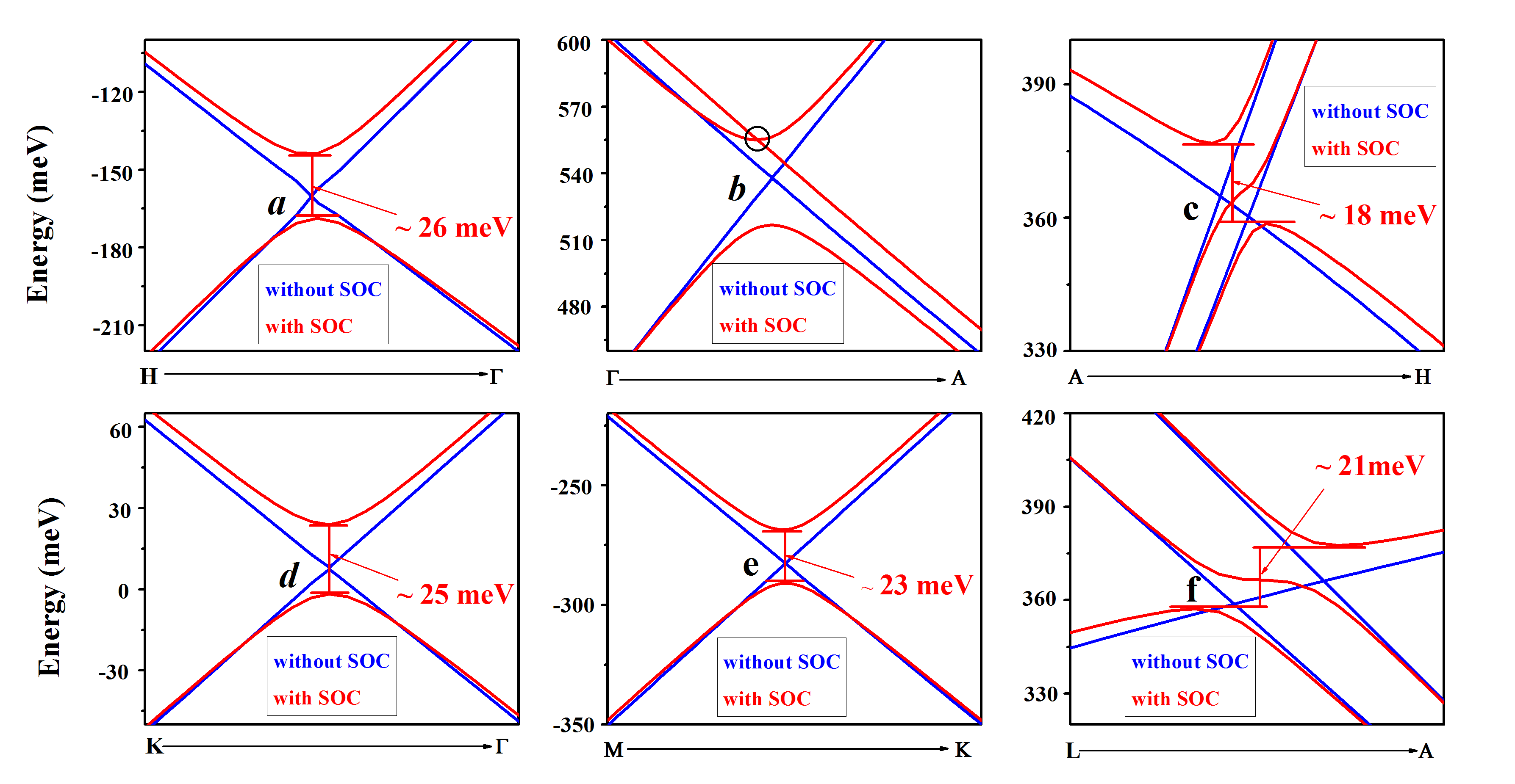
In presence of the SOC effect, the crossing points along the H-, A-H, K-, M-K and L-A lines are fully gapped, which is common in protected systems Kim et al. (2015); Fang et al. (2016). SOC makes the crossing points open gaps about 26 meV, 18 meV, 25 meV, 23 meV, and 21 meV [Fig. 5 in Appendix], respectively. The millivolt level gaps indicated that the effect of SOC on the electronic band structure of TiB2 is quite weak and can be ignored in experimental work. One thing worth mentioning is that the SOC splitting would generate a Dirac point along the direction [Fig.5b in Appendix] although it happens between the (N+2)’th and (N+3)’th bands, where N is the number of occupied bands at point in the BZ .
III Nodal net structure
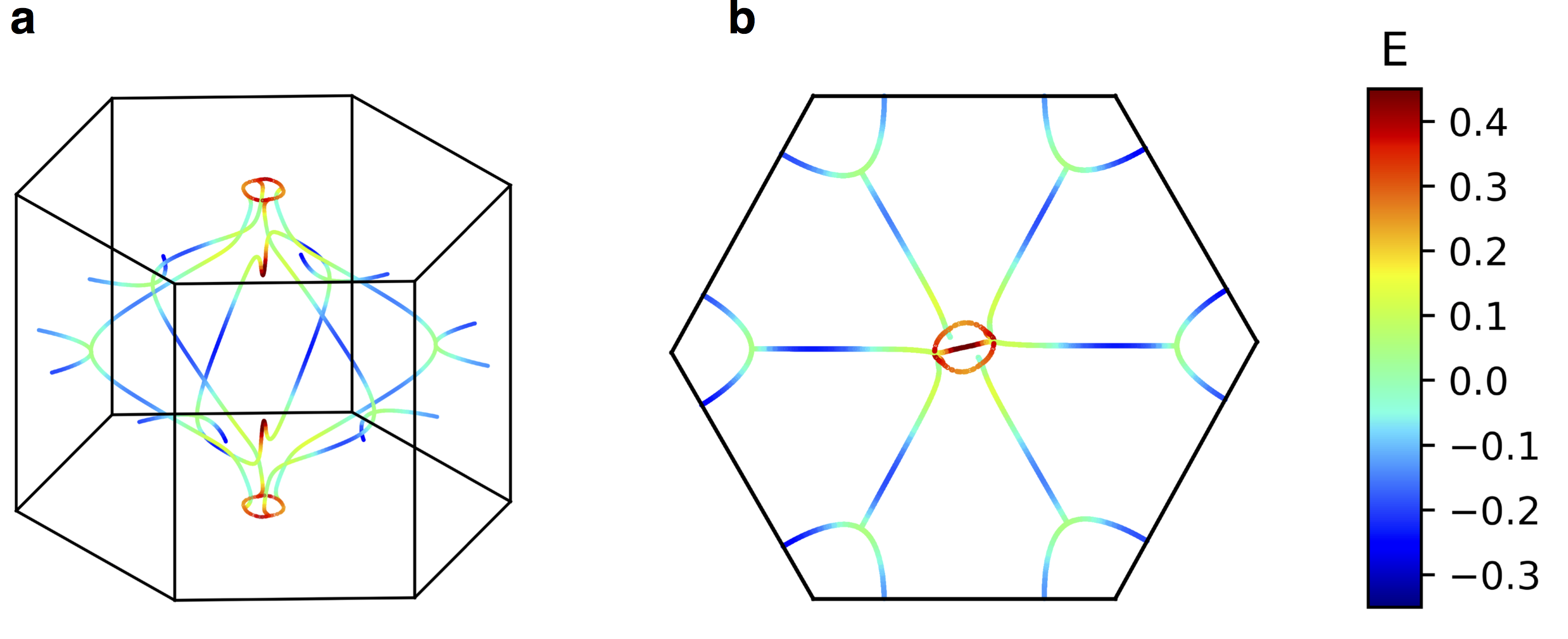
From previous studies, it is known that a nodal line system would have banana-shaped linked FSs Parker et al. (2009); Takane et al. (2016) as the NPs do not usually align at the same energy level. In other words, these banana-shape linked FSs are an indication of the existence of a nodal line structure. There is another clue to find NLSM for a symmetry protected system, i.e., if there is a band touching point close to the Fermi level, there should be a nodal line including this point Fang et al. (2016). Based on these two clues, and the BS and FS shown in Fig.2, it is clear that there is a nodal line structure in the TiB2 system. By using the symmetrical Wannier tight binding model Zhu et al. (2016) and a software package WannierTools Wu et al. (2017), we found all k-points with zero local energy gap between the N’th and (N+1)’th energy bands, where N is the number of occupied bands at the point, i.e.: . The nodal points are plotted in Fig.3, from which, the energies of nodal points are not the same which leads to the lantern-like FSs as shown in Fig.2b.
TiB2 has symmetry, which is enough to protect the existence of Dirac nodal lines in the absence of SOC. While, besides symmetry, there are another four mirror symmetries , , and in the group. Such mirror symmetries will enforce the nodal lines embed on mirror planes. Thus, these nodal lines form a interconnected nodal net structure including four classes nodal lines: A, B, C, and D. In the Appendix, with the aid of DFT calculations, it is verified that class-A,B, and D nodal lines still exist but apart from the previous mirror plane by breaking the mirror symmetries, however the class-C nodal lines will disappear.
Class-A nodal lines. Those nodal rings surrounding point, embed in the plane, which is a mirror plane of , and is shown as six arcs around point in Fig.3. The effective model at point was constructed within the little group , and shown in Eq. (45). When , , which leads to two uncoupled blocks. Those two eigenvalues of each block lead to one upward and one downward parabola. So, if the energies of the two blocks at point are different, there will be a nodal ring surrounding point.
Class-B nodal lines. Those Weyl nodes sitting on the vertical mirror planes , and , are shown as edges of the lantern in Fig.3a. We could use the effective model at point shown in Eq.(22) to prove the existence of a nodal line on such k-planes. For simplicity, we choose , a mirror perpendicular to the y-axis as an example. On this plane, , then the eigenvalues of Eq.(22) are
where , and with i=1, 2. At point, , , , . It is clear that, along , where , , which is evidence of the existence of class-C nodal lines. The nodal line in classes other than class-C could exist only if or . would leads to constraint and , which results in a touching point . However, the DFT fitting results shows that . So there is no touching point between and . Another possibility, , would lead to:
| (1) |
There are three possibilities arising from the relationship between the parameters in Eq.1
-
1.
If and , then there will be an elliptic nodal ring centered at point.
-
2.
If , then there will be an hyperbolic nodal ring.
-
3.
If and , there will be no nodal line.
According to the DFT fitting parameters, TiB2 belongs to the first class, which will have a elliptical nodal ring on three vertical mirror planes , and .
Actually, there are another three mirror symmetries , and in . Take for instance, we could perform the same analysis above by setting ; however, we have to admit that the results are the same as in the plane, i.e. there will be nodal line in the plane. The reason for this is that the model in Eq.(22) is up to second order, which will lead to isotopic effects on and . Eventually, there are not only nodal lines in the mirror planes, but also a nodal surface encompassing the point. So, in order to degenerate the nodal surface and distinguish between the and planes, we have to include higher order terms in the model, as discussed in the Appendix.D.2.
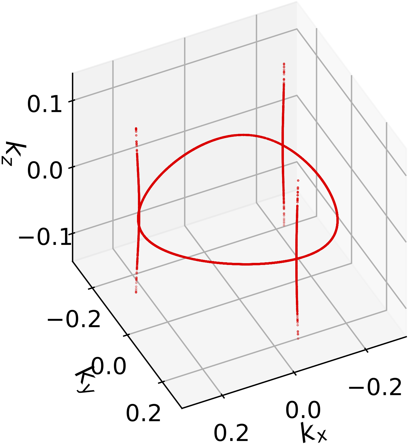
Nodal link of class-A and class-B NLs. Fig.3a shows that the class-A NL is linked with class-B NL at O point along direction, which is also shown in Fig.3c. is the overlap of and mirror planes. Eventually, the little group of O is with an additional symmetry. The 2-band effective model of O up to 2nd order of is given as
| (2) |
where and are Pauli-matrices. Since O is a nodal link point, so the mass term should be zero. Eigenvalues of Eq.2 are
| (3) |
The nodal point exists only if and , which leads to two class of NLs, one embeds in plane, which belongs to class-A NL, the other one embeds in plane, which belongs to class-B NL. It is clearly that both NLs link together at O. Taking class-A as an example, , and the other condition becomes . It is learned that is the only condition that keeps the NL. would lead the NL to be elliptic (class-A NL shown as red ring in Fig.3c), while would lead the NL to be hyperbolic (class-B NL shown as blue line in Fig.3c). It is easily to prove that the breaking down of the mirror symmetry would only move the nodal link point O and distort the NLs. However, the breaking down of symmetry would gap out all nodal points, because matrix would be introduced to Eq.2 then. So the nodal link of class-A and class-B NLs are robust under the protection of symmetry.
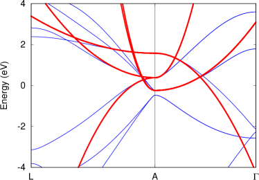
Class-C nodal lines. Actually, such nodal lines are formed by two degenerated bands along the direction, are protected by symmetry, and are shown as a segment between and points in Fig.3a. Along , there is another topological Fermion, namely the triple point Zhu et al. (2016), which is a type-A triple point according to the Ref.Zhu et al. (2016)’s definition, because the Berry phase around is zero. Such a triple point would evolve into a Dirac point in the presence of SOC [Fig.5b]. However, the topologically induced SSs of triple points would only happen in a system with SOC, and would not happen in the absence of SOC.
Class-D nodal lines. This is an isolated nodal ring at =0, and is protected by the mirror symmetry. It is easily deduced from the model (Eq.77). The eigenvalues of Eq.77 are and . since and , but and , would have a cross-point with due to its typical band inversion. The resulting nodal line is shown as an orange circle at the top plane of Fig.3a.
Topological number for the nodal net. The topological number of DNL is characterized by a quantized topological charge Kim et al. (2015), which is given by the parity of the Berry phase along a loop that interlinks with the Dirac ring [red loop in Fig.3a]. It is verified that is 1 for red loops and . The topological charge of red loops is identical to the topological charge of the green circle in Fig.3a which is composed of lines H2-H1, H1-L1, L1-L2, and L2-H2. Due to the mirror symmetry, the summation of Berry phases along H1-L1 and L2-H2 is zero. We could define a topological charge and for H2-H1 and L1-L2 respectively since they form a closed loop in k-space. From previous studies Kim et al. (2015), The topological number for a time reversal invariant loop which links two parity-invariant momenta and is related to the parity of and as
| (4) |
where is the parity for the occupied bands.
So . Since closed loop L1-L2 links and which are the parity-invariant momenta, it is verified by DFT calculations that and (see details in Appendix.E, i.e. . So the topological number for H2-H1 is . Eventually, the topological numbers are and for regions 1 and 2 shown in Fig.3b with different colors respectively. There will be odd number of nodal lines between regions 1 and 2 due to the topological number change from 0 to 1.
IV Drumhead Surface States
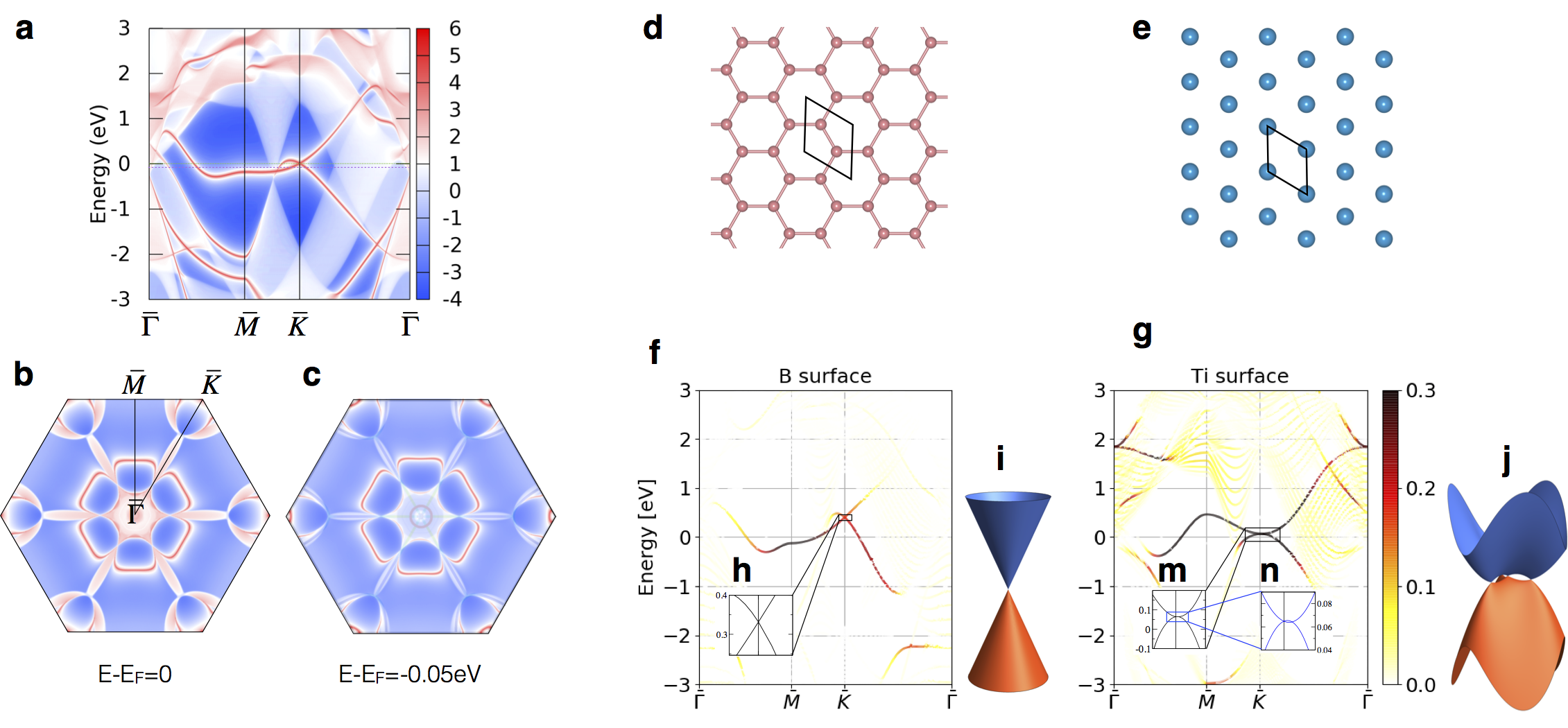
Based on previous studies Kim et al. (2015); Chan et al. (2016); Kobayashi et al. (2017), the 1D invariant partially guarantees the presence of drumhead surface states. In this section the drumhead surface states on B-terminated and Ti-terminated (001) cleavage surfaces of TiB2 are studied.
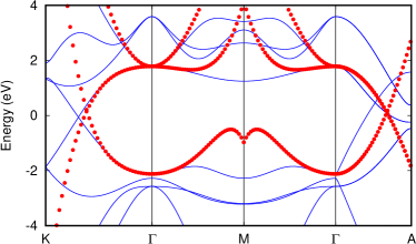
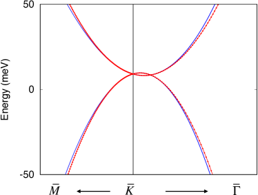
B-terminated surface structure is shown in Fig.4d, which is a honeycomb lattice like graphene. By using WannierTools Wu et al. (2017) and the method of iterative Green’s function Sancho et al. (1985) solution based on a tight-binding model (TBM), the surface state spectrum was calculated, as shown in Fig.4a-c. In Fig.4a, it is shown that between there is a drumhead surface state coming from a ”Dirac” point which is the projection of the nodal line. In region 1, those drumhead surface states form a linear Dirac cone at point, which is analogous to the Dirac cone in Graphene. SSs obtained from the TB model usually are used to explain the topological properties. To compare the SS with ARPES experimental data for further use, we use a first-principle calculations for a slab system due to that fact that a real surface system would have charge reconstructions which cannot be described by TBM. So we simulated a 20-layer slab of TiB2 with VASP. The BS is shown in Fig.4f, in which the color denotes the contributions from the orbital of the surface’s boron atoms. Basically, the DFT results are close to the TBM results. The difference is that the zero-energy point of the surface Dirac cone of DFT results is about 0.45 eV higher than that of the TBM results. Since the lattice and the orbital of the boron surface are the same as that of graphene, the effective models at point are the same, and are given as
| (5) |
where is the Fermi velocity. By fitted to the DFT calculations, is estimated to , which is about in SI units.
Ti-terminated surface structure is shown in Fig.4e, which is a hexagonal lattice of the titanium atom. The DFT calculated BS of a 20-layer slab of TiB2 with titanium in the outer surface is shown in Fig.4g, in which the color denotes contributions from orbitals of the surface’s titanium atoms. There are drumhead SSs coming from the nodal line in this case as same as B-terminated surface; however, the dispersion of SS at is different from the B-terminated surface. In Fig.4m, it seems that there is a 2D quadratic dispersed Dirac cone at point. However, by zooming into the dispersion at point, it turns out that it is a faked quadratic Dirac cone. Not only there is a linearly dispersed Dirac cone at point, but there is also a linearly dispersed Dirac cone along . Regarding the point group describing the surface structure, the effective model is obtained as
| (8) |
where and . When the quadratic terms and are missing, then Eq.(8) reduces to Eq.(5) which leads to massless linear Dirac dispersion . In the absence of linear term , Eq.(8) describes a Dirac point with parabolic energy dispersion. Such a quadratic Dirac point is unstable due to its topological number being trivial. It will split into four linear Dirac points with nontrivial topological number under the symmetry Heikkila and Volovik (2015) which leads to the linear term in Eq.(8) . Eventually, one is centered at point, the other three are connected by the symmetry (see Fig.4j). Fitting to the DFT calculated BS, we obtain the following parameters for a Ti-terminated surface: , and , in which the linear term is much weaker than the quadratic term.
The surface Dirac cone at of TiB2 with B-terminated and Ti-terminated surfaces are very similar to monolayer and bilayer graphene, which have linearly dispersed and quadratically dispersed Dirac cones respectively. The Berry phase around the linear Dirac cone is , while the Berry phase around the quadratically dispersed Dirac cone is . Such differences in the Berry phase would lead to different quantum oscillations. In Ref. Zhang et al. (2014), it was proposed that a Dirac point could be observed in monolayer TiB2; however, the Dirac point proposed in this paper could be observed on the surface of a thick slab system rather than a monolayer system.
V Conclusion
In this paper, based on first-principles calculations and model analysis, a novel symmetry protected Dirac nodal net state is recognized in AlB2-type TiB2 and ZrB2 in the absence of SOC. This complex nodal net structure is composed with four classes of NLs: A, B, C, and D, in which, class-A and class-B NLs link together at O along the direction, three class-B NLs in the vertical mirror planes terminate at A point, which is also a termination of the class-C NL. Several models for these four classes of NLs are constructed under the constraint of their symmetry which confirmed the formation of this nodal net. The topological numbers for different regions in BZ are calculated. It is noted that there are two different dispersed drumhead-like Dirac cones emerging on B-terminated and Ti-terminated surfaces, which are analogous to those of monolayer and bilayer graphene, indicating some novel surface transport properties in TiB2 and ZrB2. We believe that this work will guide further progress in understanding the novel properties of TiB2 and ZrB2, and two different terminated surfaces are good platforms to study 2D Dirac fermions. In addition, AlB2-type TiB2 and ZrB2 can be easily synthesized and provides two prototype materials to study the topological nodal net structure.
Note added.- Recently, Ref. Zhang et al. (2017) appeared, discussing some of the topological properties of metal-diboride where the nodal line around is the Class-A nodal line in the nodal net of this work.
VI Acknowledge
We acknowledged helpful discussions with X.Dai. X.F and B.W were supported by the National Natural Science Foundation of China (NSFC-51372215), C.Y and Z.S were supported by National Natural Science Foundation of China, the National 973 program of China (Grant No. 2013CB921700), Q.W was supported by Microsoft Research, and the Swiss National Science Foundation through the National Competence Centers in Research MARVEL and QSIT.
Appendix A Computational methods
In this work, the electronic properties for AlB2-type TiB2 are studied by using density functional theory (DFT) Hohenberg and Kohn (1964); Kohn and Sham (1965) as implemented in the Vienna Ab initio Simulation Package (VASP) Kresse and Furthmüller (1996, 1996); Kresse and Joubert (1999). The exchange correlation functional of Perdew-Burke-Emzerhof generalized gradient approximation (GGA-PBE) Blöchl (1994); Perdew et al. (1996) are performed. The standard version of PBE pseudo-potential is adopted in this work explicitly treating four valence electrons for the Ti atom (4d35s1) and three valence electrons for the B atom (3s23p1). A cutoff energy of 500 eV and an 11119 k-mesh are used to perform the bulk calculation. The conjugate-gradient algorithm is used to relax the ions, and the convergence thresholds for total energy and ionic force component are chosen as 110-7 eV and 0.001 eV/.
For the slab calculations (Fig.4f-g), the thickness of the B-terminated slab is 20 layers of titanium and 21 layers of boron, while the thickness of the Ti-terminated slab is 20 layers of titanium and 19 layers of toron. A centered k mesh and a 14-thick vacuum are used in the DFT simulations. The surface are fully relaxed with energy convergence up to 110-7 eV and force up to 0.001 eV/.
The nodal-net searching and surface states spectrum calculations shown in Fig.4a-c are done using the open-source software WannierTools Wu et al. (2017) which is based on Wannier tight binding model (WTBM) constructed with Wannier90 Mostofi et al. (2008). Ti , and B orbitals are used as initial projectors for WTBM construction. WTBMs constructed with Wannier90 do not exactly fulfil all crystal symmetries which is very important for nodal points searching because usually nodal points are protected by crystal symmetries except Weyl points. The WTBM is symmetrized to be compatible with the crystal symmetry using the method described in Red. Zhu et al. (2016).
Appendix B band structure and Fermi surface of AlB2-type ZrB2
In general, ZrB2 is often compared with TiB2. The structure of AlB2-type ZrB2 also has hexagonal structure with a space group of P6/mmm (No.191). Its optimized lattice constants are a=b=3.1748(3) and c=3.5579(7) , which is slightly larger than those of TiB2. As shown in Fig.6a, there are also six band crossing points along the high-symmetry path similar with TiB2. Among them, Zr 4d states are the main contribution orbitals for these six band crossing points. The Zr-dxz and Zr-dxy orbitals are much higher than the Fermi level. From Figs. 6b and c, the Fermi surface of ZrB2 is sightly different from that of TiB2. The circling surface around A point is disappeared in the Fermi surface of ZrB2. The main part of the lantern-like Fermi surface of ZrB2 is basically consistent with the Fermi surface of TiB2, which also shows a nodal-net feature.
Appendix C Nodal net structure of TiB2 without vertical mirror planes
Since the nodal net of TiB2 is symmetry protected, any perturbations that preserve the inversion symmetry can only distort the nodal-net but not destroy them. As an example,we apply a uniaxial strain (compression 1) along the [100] crystal direction. After deformation, the structure of AlB2-type TiB2 belongs to space group of C2/m (No. 12), which just preserves the Mz mirror reflection symmetry. As a result, as shown in Fig.7, it is found that the class-A nodal line still embeds in the plane, one of the class-B nodal line become isolated with the other two class-B nodal lines which link with the class-D nodal line that embeds in the plane, while the class-D nodal line along disappears because it is protected by symmetry which is destroyed under such strain. Thus, the nodal net in TiB2 is robustly stable, which does not requires the protection of mirror symmetry.
Appendix D Effective model
We derive several models describing the bulk bands in the vicinity of , A, and K in the 3D BZ, and a for surface states at point in 2D BZ. The models are used to get a better understanding of the surface states and the nodal net structures, and would be useful for further investigations of Landau level and quantum transport properties.
The models were calculated using the kdotp_symmetry code, which implements the method described in Ref. Gresch et al. (2017), basically, there are two things that should be prepared before applying kdotp_symmetry. Firstly, we identify the little group of a high symmetry point of which we want to construct a low energy effective model, and get the generators of little group . Secondly, we identify the representations of on the basis of the eigenvectors at the selected high-symmetry points. Then kdotp_symmetry will produce the model under the constraint
| (9) |
where D(R) is the representation matrix of symmetry operator .
D.1 model at point
The little point group at Gamma point of bulk TiB2 is plus TR symmetry (see Table 76 of Ref.Koster (1962)). There are three generators of including spatial-inversion , 2-fold rotation and 6-fold rotation . From the fat-band analysis of Fig.2, the relevant bands come from which belongs to the representation, and orbitals which form the basis of its representation. The representations of group generators according to the symmetrical basis {(+i)/, (-i)/ , } are given by
| (10) | |||
| (14) | |||
| (18) |
where, is the complex conjugation operator. Considering these symmetries, and the constraint of Eq.(9), a 3-band model up to second order of k around point for bulk TiB2 is given by
| (22) |
where , .
As mentioned in the main text, Eq.(22) with only second order momentum would lead to a nodal surface other than the nodal line structure. To distinguish the difference between and directions, we have to introduce the sixth order of , in the plane, and introduce a fourth order of , in the off-diagonal part, so eventually, the new model is given by
| (26) |
where , .
By fitting to the DFT band structure of TiB2, the parameters in Eq.(26) are obtained: , , , , , , , , , , and . The comparison between DFT bands and bands is shown in Fig.8
The nodal line structure around point calculated from Eq.26 with the DFT fitted parameters is shown in Fig.9a. It is shown that the nodal net close to point is very similar to Fig.3, the class-A, class-B, and class-C nodal lines are captured successfully; however the nodal line beyond the nexus point is not captured. That is because the nexus point is at the boundary of the BZ, which is related to an infinity in the model. The position of the nexus point could be tuned by changing in Eq.26. In Fig.9c, it is shown that the nexus point would disappear if was very large. The nodal line in the mirror plane could be shown if the fourth and sixth order terms in Eq.26 become smaller (Fig.9b).
D.2 model at K point
The little group at K point in the TiB2 is (see Table 65 of Ref.Koster (1962)), of which there are three generators including horizontal mirror , 2-fold rotation and 3-fold rotation . Around K point, the relevant representations are , of which the basis are and . Taking the symmetrical orbitals { , -} and { } as a basis, where is the complex Spherical harmonic function, the representations of the generators are given by
| (27) | |||
| (32) | |||
| (37) |
Considering these symmetries above and the constraint of Eq.(9), a 4-band model up to second order of k around point in bulk TiB2 is given by
| (42) |
where and . The fitted parameters of TiB2 are , , , , , , , , , , , . The comparison between DFT bands and bands is shown in Fig. 13.
In order to analyse the nodal line structure, Eq.(42) can be written into two blocks
| (45) |
where
| (48) | ||||
| (51) | ||||
| (54) |
With the fitted parameters, we find that our model not only describes the nodal line surrounding point, but can also predict part of the nodal line in the vertical mirror plane.
D.3 model at A point
For the little group at A (see Table 76 of Ref.Koster (1962)), relevant representations are and , which constitutes {}, {, } and{, }. By symmetrization of those orbitals according to the group, the symmetrical basis are chosen as , , -, - and , and the related representations of its generators are given by
| (55) | |||
| (60) | |||
| (61) | |||
| (66) |
The constructed model is given by
| (72) |
where with . The fitted parameters are , , , , , , , , , , , , . The fitted band is shown in Fig.12.
Particularly, when the effective , this means that bulk , Eq.(72) decouples into three block diagonal matrices. From Fig.2, it is shown that along , band crossing happens between and the combination of and . i.e. we only have to consider the following block of Eq.(72)
| (77) |
D.4 model for surface states at points
The little group at point of slab system TiB2 is , which has two generators and . According to the DFT calculations, it was determined that the surface state at belongs to (see Table 49 of Ref.Koster (1962)) representation of . On the basis of complex orbitals, the related representations of its generators are given by
| (82) |
Considering these symmetries above and the constraint of Eq.(9), a 2-band model up to the second order of k around point for surface states is given by
| (85) |
where and . The linear part of Eq.(85) leads to massless Dirac dispersion . The combination of the linear term and the quadratic term leads to 3-fold rotation symmetry of the energy dispersion. Fitting to DFT calculation band structure, We obtain the following parameters for Ti-terminated surface: , and for the B-terminated surface A=1.5, B=0, C=0.
Appendix E Parities at TRIMs
The parities of the occupied bands of TiB2 at TRIMs are listed in Table.1. It is noted that there are six occupied bands at , and five occupied bands at other TRIMs. The product of the parities of the occupied bands at and are 1, which leads to and .
| TRIM | parity | Total | |||||
|---|---|---|---|---|---|---|---|
| (0.0, 0.0, 0.0) | + | + | + | - | + | - | |
| (0.5, 0.0, 0.0) | + | - | - | + | + | + | |
| (0.0, 0.5, 0.0) | + | - | - | + | + | + | |
| (0.0, 0.0, 0.5) | - | + | - | - | + | + | - |
| (0.5, 0.5, 0.0) | + | - | - | + | + | + | |
| (0.0, 0.5, 0.5) | + | - | + | + | - | + | |
| (0.5, 0.0, 0.5) | + | - | + | + | - | + | |
| (0.5, 0.5, 0.5) | + | - | + | + | - | + |
References
- Chiu et al. (2016) C. K. Chiu, J. C. Y. Teo, A. P. Schnyder, and S. Ryu, Rev. Mod. Phys. 88, 035005 (2016).
- Bzdušek et al. (2016) T. Bzdušek, Q. Wu, A. Rüegg, M. Sigrist, and A. A. Soluyanov, Nature 538, 75 (2016).
- Kobayashi et al. (2017) S. Kobayashi, Y. Yamakawa, Y. Ai, T. Inohara, Y. Okamoto, and Y. Tanaka, arxiv:1703.03587 (2017).
- Burkov et al. (2011) A. A. Burkov, M. D. Hook, and L. Balents, Phys. Rev. B 84, 235126 (2011).
- Wan et al. (2011) X. Wan, A. M. Turner, A. Vishwanath, and S. Y. Savrasov, Phys. Rev. B 83, 205101 (2011).
- Weng et al. (2015a) H. Weng, C. Fang, Z. Fang, B. A. Bernevig, and X. Dai, Phys. Rev. X 5, 011029 (2015a).
- Huang et al. (2015a) S.-M. Huang, S.-Y. Xu, I. Belopolski, C.-C. Lee, G. Chang, B. Wang, N. Alidoust, G. Bian, M. Neupane, C. Zhang, S. Jia, A. Bansil, H. Lin, and M. Z. Hasan, Nature Communications 6, 7373 EP (2015a).
- Xu et al. (2015) S.-Y. Xu, I. Belopolski, N. Alidoust, M. Neupane, G. Bian, C. Zhang, R. Sankar, G. Chang, Z. Yuan, C.-C. Lee, S.-M. Huang, H. Zheng, J. Ma, D. S. Sanchez, B. Wang, A. Bansil, F. Chou, P. P. Shibayev, H. Lin, S. Jia, and M. Z. Hasan, Science 349, 613 (2015).
- Lv et al. (2015) B. Q. Lv, H. M. Weng, B. B. Fu, X. P. Wang, H. Miao, J. Ma, P. Richard, X. C. Huang, L. X. Zhao, G. F. Chen, Z. Fang, X. Dai, T. Qian, and H. Ding, Phys. Rev. X 5, 031013 (2015).
- Soluyanov et al. (2015) A. A. Soluyanov, D. Gresch, Z. Wang, Q. Wu, M. Troyer, X. Dai, and B. A. Bernevig, Nature 527, 495 (2015).
- Novoselov et al. (2005) K. S. Novoselov, A. K. Geim, S. Morozov, D. Jiang, M. Katsnelson, I. Grigorieva, S. Dubonos, and A. Firsov, Nature 438, 197 (2005).
- Wang et al. (2012) Z. Wang, Y. Sun, X. Chen, C. Franchini, G. Xu, H. Weng, X. Dai, and Z. Fang, Phys. Rev. B 85, 195320 (2012).
- Liu et al. (2014) Z. K. Liu, B. Zhou, Y. Zhang, Z. J. Wang, H. M. Weng, D. Prabhakaran, S. K. Mo, Z. X. Shen, Z. Fang, X. Dai, Z. Hussain, and Y. L. Chen, Science 343, 864 (2014).
- Young et al. (2012) S. M. Young, S. Zaheer, J. C. Y. Teo, C. L. Kane, E. J. Mele, and A. M. Rappe, Phys. Rev. Lett. 108, 140405 (2012).
- Zhu et al. (2016) Z. Zhu, G. W. Winkler, Q. Wu, J. Li, and A. A. Soluyanov, Phys. Rev. X 6, 031003 (2016).
- Weng et al. (2016) H. Weng, C. Fang, Z. Fang, and X. Dai, Phys. Rev. B 93, 241202 (2016).
- Chang et al. (2016) G. Chang, S.-Y. Xu, S.-M. Huang, D. S. Sanchez, C.-H. Hsu, G. Bian, Z.-M. Yu, I. Belopolski, N. Alidoust, H. Zheng, T.-R. Chang, H.-T. Jeng, S. A. Yang, T. Neupert, H. Lin, and M. Z. Hasan, , 24 (2016), arXiv:1605.06831 .
- Bradlyn et al. (2016) B. Bradlyn, J. Cano, Z. Wang, M. G. Vergniory, C. Felser, R. J. Cava, and B. A. Bernevig, Science 353, aaf5037 (2016).
- Hu et al. (2016) J. Hu, Z. Tang, J. Liu, X. Liu, Y. Zhu, D. Graf, K. Myhro, S. Tran, C. N. Lau, J. Wei, and Z. Mao, Phys. Rev. Lett. 117, 016602 (2016).
- Bian et al. (2016) G. Bian, T. R. Chang, H. Zheng, S. Velury, S. Y. Xu, T. Neupert, C. K. Chiu, S. M. Huang, D. S. Sanchez, I. Belopolski, N. Alidoust, P.-J. Chen, G. Chang, A. Bansil, H. T. Jeng, H. Lin, and M. Z. Hasan, Phys. Rev. B 93, 121113 (2016).
- Yu et al. (2017a) R. Yu, Q. Wu, Z. Fang, and H. Weng, arxiv:1701.08502 (2017a).
- Liang et al. (2016) Q. Liang, J. Zhou, R. Yu, Z. Wang, and H. Weng, Phys. Rev. B 93, 085427 (2016).
- Zhang et al. (2005) Y. Zhang, Y. W. Tan, H. L. Stormer, and P. Kim, Nature 438, 201 (2005).
- Son and Yamamoto (2012) D. T. Son and N. Yamamoto, Phys. Rev. Lett. 109, 181602 (2012).
- Song et al. (2016) Z. Song, J. Zhao, Z. Fang, and X. Dai, Phys. Rev. B 94, 214306 (2016).
- Vazifeh and Franz (2013) M. M. Vazifeh and M. Franz, Phys. Rev. Lett. 111, 027201 (2013).
- Fukushima et al. (2008) K. Fukushima, D. E. Kharzeev, and H. J. Warringa, Phys. Rev. D 78, 074033 (2008).
- Ali et al. (2014) M. N. Ali, J. Xiong, S. Flynn, J. Tao, Q. D. Gibson, L. M. Schoop, T. Liang, N. Haldolaarachchige, M. Hirschberger, N. P. Ong, and R. J. Cava, Nature 514, 205 (2014).
- Zyuzin and Burkov (2012) A. A. Zyuzin and A. A. Burkov, Phys. Rev. B 86, 115133 (2012).
- Hosur and Qi (2013) P. Hosur and X. Qi, Comptes Rendus Physique 14, 857 (2013).
- Huang et al. (2015b) X. Huang, L. Zhao, Y. Long, P. Wang, D. Chen, Z. Yang, H. Liang, M. Xue, H. Weng, Z. Fang, X. Dai, and G. Chen, Phys. Rev. X 5, 031023 (2015b).
- Carmier and Ullmo (2008) P. Carmier and D. Ullmo, Phys. Rev. B 77, 245413 (2008).
- Yan et al. (2017) Z. Yan, R. Bi, H. Shen, L. Lu, S. Zhang, and Z. Wang, arxiv:1704.00655 (2017).
- Fang et al. (2016) C. Fang, H. Weng, X. Dai, and Z. Fang, Chinese Physics B 25, 9 (2016).
- Yu et al. (2017b) R. Yu, Z. Fang, X. Dai, and H. Weng, Frontiers of Physics 12, 127202 (2017b).
- Hirayama et al. (2017) M. Hirayama, R. Okugawa, T. Miyake, and S. Murakami, Nature Communications 8, 14022 (2017).
- Cheng et al. (2017) Y. Cheng, X. Feng, X. Cao, B. Wen, Q. Wang, Y. Kawazoe, and P. Jena, Small 13, 1602894 (2017).
- Kim et al. (2015) Y. Kim, B. J. Wieder, C. L. Kane, and A. M. Rappe, Phys. Rev. Lett. 115, 036806 (2015).
- Fang et al. (2015) C. Fang, Y. Chen, H.-Y. Kee, and L. Fu, Phys. Rev. B 92, 081201 (2015).
- Heikkila and Volovik (2015) T. T. Heikkila and G. E. Volovik, New Journal of Physics 17, 1 (2015).
- Hyart and Heikkila (2016) T. Hyart and T. T. Heikkila, arxiv:1604.06357 (2016).
- Weng et al. (2015b) H. Weng, Y. Liang, Q. Xu, R. Yu, Z. Fang, X. Dai, and Y. Kawazoe, Phys. Rev. B 92, 045108 (2015b).
- Yu et al. (2015) R. Yu, H. Weng, Z. Fang, X. Dai, and X. Hu, Phys. Rev. Lett. 115, 036807 (2015).
- Chang and Yee (2017) P. Chang and C. Yee, arxiv:1704.01948 (2017).
- Chen et al. (2017) W. Chen, H. Lu, and J. Hou, arxiv:1703.10886 (2017).
- Chiu and Schnyder (2014) C. Chiu and A. P. Schnyder, Phys. Rev. B 90, 205136 (2014).
- Waśkowska et al. (2011) A. Waśkowska, L. Gerward, J. S. Olsen, K. R. Babu, G. Vaitheeswaran, V. Kanchana, A. Svane, V. Filipov, G. Levchenko, and A. Lyaschenko, Acta Materialia 59, 4886 (2011).
- Okamoto et al. (2010) N. L. Okamoto, M. Kusakari, K. Tanaka, H. Inui, and S. Otani, Acta Materialia 58, 76 (2010).
- Kumar et al. (2012) R. Kumar, M. Mishra, B. Sharma, V. Sharma, J. Lowther, V. Vyas, and G. Sharma, Computational Materials Science 61, 150 (2012).
- Wang et al. (2011) H. Wang, F. Xue, N. H. Zhao, and D. J. Li, in Advances in Composites, Advanced Materials Research, Vol. 150 (Trans Tech Publications, 2011) pp. 40–43.
- Altmann and Herzig (1994) S. Altmann and P. Herzig, Point-group theory tables, Oxford science publications (Clarendon Press, 1994).
- Cornwall (1999) J. M. Cornwall, Phys. Rev. D 59, 125015 (1999).
- Post et al. (1954) B. Post, F. W. Glaser, and D. Moskowitz, Acta Metallurgica 2, 20 (1954).
- Milman and Warren (2001) V. Milman and M. C. Warren, Journal of Physics: Condensed Matter 13, 5585 (2001).
- Tanaka and Ishizawa (1980) T. Tanaka and Y. Ishizawa, Journal of Physics C: Solid State Physics 13, 6671 (1980).
- Parker et al. (2009) D. Parker, M. G. Vavilov, A. V. Chubukov, and I. I. Mazin, Phys. Rev. B 80, 100508 (2009).
- Takane et al. (2016) D. Takane, Z. Wang, S. Souma, K. Nakayama, C. X. Trang, T. Sato, T. Takahashi, and Y. Ando, Phys. Rev. B 94, 121108 (2016).
- Wu et al. (2017) Q. Wu, S. Zhang, H. Song, M. Troyer, and A. A. Soluyanov, arxiv:1703.07789 (2017).
- Chan et al. (2016) Y. Chan, C. Chiu, M. Y. Chou, and A. P. Schnyder, Phys. Rev. B 93, 205132 (2016).
- Sancho et al. (1985) M. P. L. Sancho, J. M. L. Sancho, J. M. L. Sancho, and J. Rubio, Journal of Physics F: Metal Physics 15, 851 (1985).
- Zhang et al. (2014) L. Z. Zhang, Z. F. Wang, S. X. Du, H. J. Gao, and F. Liu, Phys. Rev. B 90, 161402 (2014).
- Zhang et al. (2017) X. Zhang, Z. Yu, X. Sheng, H. Y. Yang, and S. A. Yang, arxiv:1704.03703 (2017).
- Hohenberg and Kohn (1964) P. Hohenberg and W. Kohn, Phys. Rev. 136, B864 (1964).
- Kohn and Sham (1965) W. Kohn and L. J. Sham, Phys. Rev. 140, A1133 (1965).
- Kresse and Furthmüller (1996) G. Kresse and J. Furthmüller, Computational Materials Science 6, 15 (1996).
- Kresse and Furthmüller (1996) G. Kresse and J. Furthmüller, Phys. Rev. B 54, 11169 (1996).
- Kresse and Joubert (1999) G. Kresse and D. Joubert, Phys. Rev. B 59, 1758 (1999).
- Blöchl (1994) P. E. Blöchl, Phys. Rev. B 50, 17953 (1994).
- Perdew et al. (1996) J. P. Perdew, K. Burke, and M. Ernzerhof, Phys. Rev. Lett. 77, 3865 (1996).
- Mostofi et al. (2008) A. A. Mostofi, J. R. Yates, Y. S. Lee, I. Souza, D. Vanderbilt, and N. Marzari, Computer physics communications 178, 685 (2008).
- Gresch et al. (2017) D. Gresch, Q. Wu, G. W. Winkler, and A. A. Soluyanov, New Journal of Physics 19, 035001 (2017).
- Koster (1962) G. F. Koster, Properties of thirty-two point groups (M.I.T. Press, 1962).