Hardware for Dynamic Quantum Computing
Abstract
We describe the hardware, gateware, and software developed at Raytheon BBN Technologies for dynamic quantum information processing experiments on superconducting qubits. In dynamic experiments, real-time qubit state information is fedback or fedforward within a fraction of the qubits’ coherence time to dynamically change the implemented sequence. The hardware presented here covers both control and readout of superconducting qubits. For readout we created a custom signal processing gateware and software stack on commercial hardware to convert pulses in a heterodyne receiver into qubit state assignments with minimal latency, alongside data taking capability. For control, we developed custom hardware with gateware and software for pulse sequencing and steering information distribution that is capable of arbitrary control flow on a fraction superconducting qubit coherence times. Both readout and control platforms make extensive use of FPGAs to enable tailored qubit control systems in a reconfigurable fabric suitable for iterative development.
I Introduction
Building a large scale quantum information processor is a daunting technology integration challenge. Most current experiments demonstrate static circuits, where a pre-compiled sequence of gates is terminated by qubit measurements. In some cases, conditional control flow is emulated by postselecting data on certain measurement outcomes Chow et al. (2014), or by gating duplicate hardware behind a switch to handle a single branch in a pulse program Steffen et al. (2013); Ristè et al. (2013). However, because of the need for quantum error correction Gottesman (2009), fault-tolerant quantum computation is inevitably an actively controlled process. This active control may manifest as: continuous entropy removal from the system via active reset Aharonov et al. (1996), active error correction after decoding syndrome measurements, Pauli frame updates for subsequent pulses after state injection Bravyi and Kitaev (2005); Knill (2005), or non-deterministic “repeat-until-success” Paetznick and Svore (2014) gates. The community is now tackling the challenge of dynamically steering an experiment within the coherence time of the qubits Ristè et al. (2012); Campagne-Ibarcq et al. (2013); Pfa (2014); Ofek et al. (2016). For superconducting qubits this coherence time—although continuously improving—is currently 50–100. To achieve control fidelities compatible with expected thresholds for fault-tolerant quantum computation Knill (2005); Raussendorf and Harrington (2007), the feedback/feedforward time must be less than 1% of this coherence time, or on the order of a few hundred nanoseconds.
Superconducting qubit control systems send a coordinated sequence of microwave pulses, with durations from tens to hundreds of nanoseconds, down coaxial lines of a dilution refrigerator to implement both control and readout of the qubits. Currently, the microwave pulses are produced and recorded at r.f. frequencies by mixing up or down with a microwave carrier, allowing commonly available GS/s digital-to-analog (DAC) and analog-to-digital (ADC) converters to be used. In the circuit quantum electrodynamics (QED) platform Schuster (2007), the qubit state is encoded in the amplitude and phase of a measurement pulse that interacts with a microwave cavity coupled dispersively to the qubit. This microwave pulse is typically captured with a room temperature receiver, then converted into a qubit state assignment via a digital signal processing (DSP) pipeline. Programming the control sequences for dynamic experiments also requires a supporting framework from the pulse sequencing language and hardware. Conventional arbitrary waveform generator (AWG) sequence tables are far too restrictive to support control flow beyond simple repeated sections. The desired control flow requires conditional execution, loops with arbitrary nesting, and subroutines for code reuse.
The required timescale for active control is beyond the capabilities of a software solution running on a general purpose operating system; however, it is within reach of custom gateware running on field programmable gate arrays (FPGAs) directly connected to analog digital converters for both qubit control and measurement. Many groups in superconducting and ion trap quantum computing have turned to this approach and started to build a framework of controllers and actuators. For trapped ions, the Advanced Real-Time Infrastructure for Quantum physics (ARTIQ) Bourdeauducq et al. (2016) is a complete framework of hardware, gateware, and software for controlling quantum information experiments. However, ARTIQ’s control flow architecture uses general purpose CPUs implemented in FPGA fabric, so called soft-core CPUs, which cannot maintain the event rate required by superconducting qubits (gates are 1–2 orders of magnitude slower in ion traps). Researchers at UCSB/Google Chen et al. (2012); Jeffrey et al. (2014), ETH Zurich Steffen et al. (2013), TU Delft Ristè et al. (2013); Bultink et al. (2016), and Yale Ofek et al. (2016) have also built superconducting qubit control and/or readout platforms using FPGAs, and even explored moving them to the cryogenic stages Homulle et al. (2016); Conway Lamb et al. (2016), but have generally not made these tools available to the broader quantum information community.
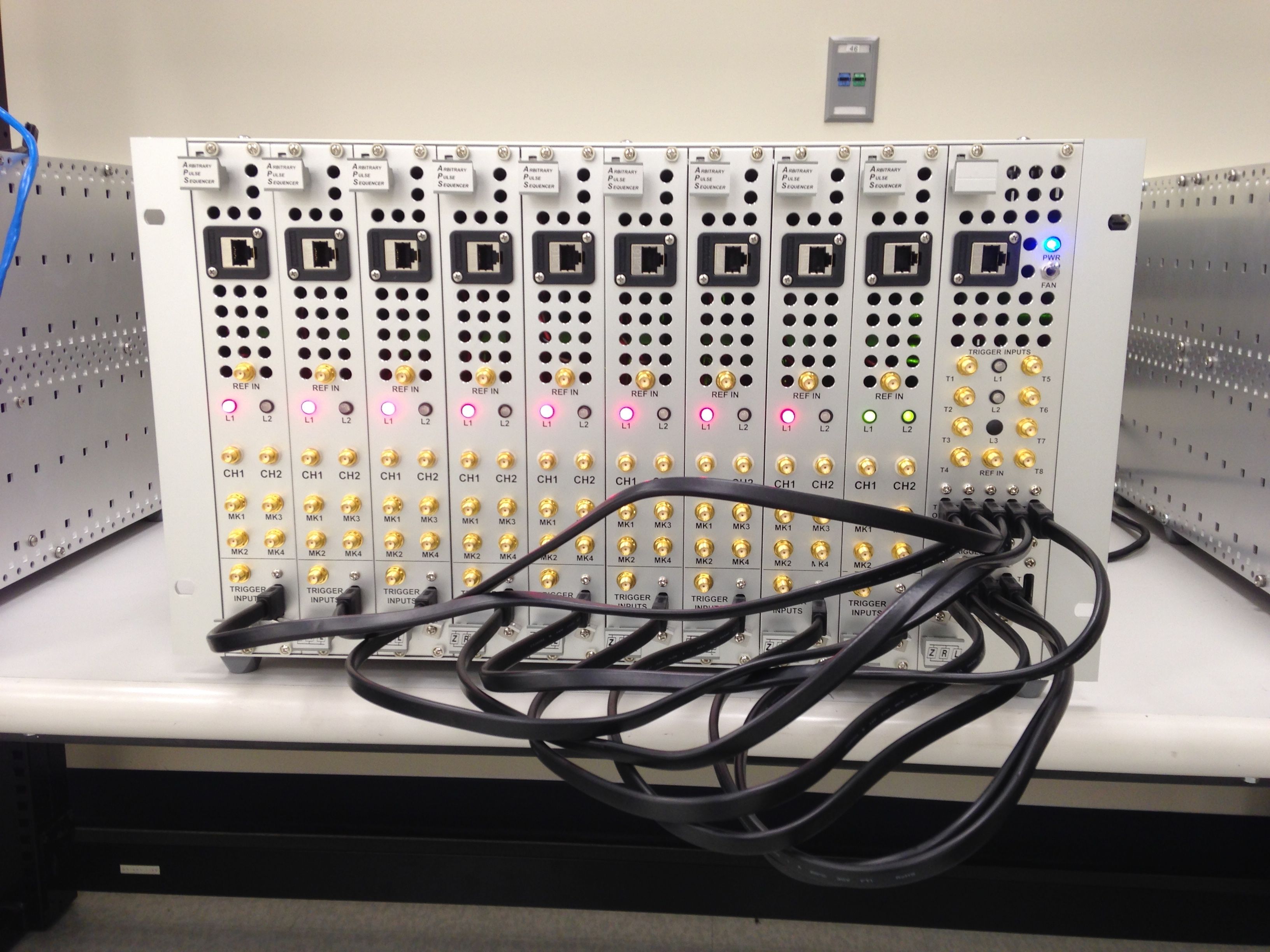
In this work, we introduce the QDSP framework and Arbitrary Pulse Sequencer 2 (APS2) for qubit readout and control, respectively. QDSP implements state assignment and data recording in FPGA gateware for a commercially available receiver/exciter system (the Innovative Integration X6-1000M, also used in the Yale workOfek et al. (2016)). We show how latency can be minimized for rapid qubit state decisions by consolidating many of the conventional DSP stages into one. The APS2, shown in Fig. 1, has gateware designed to naturally support arbitrary control flow in quantum circuit sequences on superconducting qubits. For circuits involving multiple qubits, state information from many qubits must be collated and synthesized into a steering decision by a controller. To this end we designed the Trigger Distribution Module (TDM) to capture up to eight channels of qubit state information, execute arbitrary logic on an FPGA, and then distribute steering information to APS2 output modules over low-latency serial data links. All the systems presented here are either commercially available or full source code for gateware and drivers has been posted under a permissive open-source license.
To validate the developed gateware and hardware we demonstrate multi-qubit routines and quantum gates that require feedback and feedforward: active qubit initialization, entanglement generation through measurement, and measurement-based logic gates. Although these are specific examples, they are implemented in a general framework that enables arbitrary steering of quantum circuits. Furthermore, with appropriate quantum hardware, different circuits are all achieved without re-wiring the control systems, but simply by executing different programs on the APS2 and TDM.
II Qubit State Decisions in Hardware
The first requirement for quantum feedback is extracting qubit state decisions with minimal latency. Typical superconducting qubit measurements involve sending a microwave pulse to a readout resonator, recording the reflected/transmitted signal, filtering noise and other out-of-band signals, and reducing the record to a binary decision about the qubit state. Conventionally, this is accomplished with a superheterodyne transmitter and receiver operating with an intermediate frequency (IF) of 10s of MHz which allows the IF stages to be handled digitally.
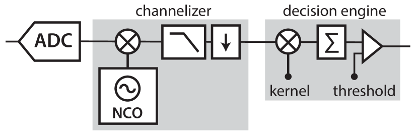
Since many measurement channels may be frequency multiplexed onto the same line, the DSP chain involves several stages of filtering to channelize the signal. This involves mixing the captured record with a continuous wave (CW) IF signal—produced by a numerically controlled oscillator (NCO)—and several low-pass filtering and decimation stages to recover a baseband complex-valued phasor as a function of time (Fig. 2). This complex-time series is then integrated with a kernel, which may be a simple box car filter or optimized to maximally distinguish the qubit states Gambetta et al. (2007); Ryan et al. (2015). A final qubit state is determined by thresholding the integrated value. These receiver functions, which have frequently been implemented in software, are ideally suited to DSP resources available in modern FPGAs. Moving these functions into custom gateware has additional benefits for parallel processing of simultaneous measurements, reducing CPU load on the control PC, and greatly reducing latency of qubit state decisions.
II.1 Filter design
The design of the channel filter for qubit readout is the result of balancing several considerations:
-
1.
bandwidth of the channel—should be some small multiple of the resonator bandwidth, ;
-
2.
stopband attenuation sufficient to remove channel crosstalk;
-
3.
numerical stability—particularly when implemented with either single precision or fixed-point representation;
-
4.
latency;
-
5.
computational resources.
Some of these criteria are in competition with each other. For instance, one may decrease channel crosstalk by using a higher-order filter, but this comes at the expense of increased latency and computational cost. Qubit devices used in our lab have typical resonator bandwidths of . In the high fidelity, QND readout regime we have noticed harmonic content in the readout signal at multiples of the dispersive shift, , that extends the signal bandwidth by roughly a factor of 2. Consequently, we have designed channel filters with bandwidth. The downconversion structure of Fig. 2 selects symmetric channels around the IF frequency; thus, a channel corresponds to a filter with a bandwidth of . We also want sufficient stopband attenuation to limit channel crosstalk. We have chosen the stopband attenuation such that a fullscale signal in an adjacent channel is suppressed below the least-significant bit of the selected channel. Given the signed 12-bit ADCs on our target platform, this requires stopband attenuation.
The relatively narrow bandwidth of the readout channels compared to the 1 GS/s sampling rate of the ADC leads to numerical stability problems in fixed-point or single-precision designs. Re-expressed as a relative bandwidth, the MHz channel described above has . However, it is difficult to construct stable filters with normalized bandwidth . This may be solved by cascading several polyphase decimating filters to boost the 3 dB bandwidth of the later stages— this brings an additional benefit of reducing the computational resources.
II.2 Fast Integration Kernels
While the complete time-trace of the measurement record is a useful debugging tool for observing and understanding the cavity response from the two (or more) qubit states, a conventional channelizer with multiple stages of signal processing (NCO mixing, filtering and integrating) forces an undesirable latency. Take a typical example of channels spaced apart. A Parks-McClellan McClellan and Parks (1973) designed FIR low-pass filter for a sampling rate with a pass band from and stop-band from with suppression requires at least 86 taps. At a typical FPGA clock speed of this results in 100s of nanoseconds of latency. However, the qubit state decision reduces the time dimension to a single value with a kernel integrator. The intermediate filtering stage is thus superfluous if we can construct an appropriate frequency-selective kernel. This crucial insight enables us to drive down the signal processing latency to a few clock cycles.
More formally, consider the discrete time measurement record for a total of length samples. Applying the DSP chain of Fig. 2 , the final single complex value qubit state signal (before thresholding and ignoring decimation for simplicity) is:
| (1) |
where the demodulation frequency is , the channel is selected with an -tap FIR filter with coefficients and a final kernel integration is applied for the length of the record . The nested sum and product can be expanded and the terms collected into a single kernel integration, with a modified kernel
| (2) |
Thus, the three-stage pipeline of Fig. 2 is reduced into a single-stage pipeline consisting solely of the kernel integration step.
This reduction of the pipeline to a single stage has substantial advantages for DSP latency. In particular, the FIR filter block of the three-stage pipeline has a minimum latency of N clock cycles for a N-tap filter. As discussed above, this can be 100s of nanoseconds and this single filter stage consumes the entire latency budget in a single step. By constrast, the DSP pipeline of Eq. 2 can be achieved with 1-3 clock cycles of latency on the FPGA, or .
While equations 1 and 2 demonstrate the mathematical equivalence of the 1-stage and 3-stage DSP pipelines, in practice it is not necessary to transform a baseband integration kernel via Eq. 2. Instead, one can use the average unfiltered (IF) response at the ADC after preparing a qubit in and to construct a matched filter Ryan et al. (2015). The frequency response of the resulting filter will match that of the measurement pulse itself. Consequently, as long as the measurement pulse is itself band-limited — which should always be the case with an appropriately designed dispersive cavity measurement — the resulting matched filter will also optimally “channelize” the ADC input and suppress interference from other multiplexed qubit measurement channels.
II.3 Hardware Implementation
To minimize overall latency, we implement our QDSP qubit readout system in custom FPGA gateware (QDSP - github.com/BBN-Q/BBN-QDSP-X6) and software drivers (libx6 - github.com/BBN-Q/libx6/) for a commercially available hardware platform (Innovative Integration X6-1000M). The X6 hardware provides two 12-bit 1 GS/s ADCs and four 16-bit 500 MS/s DACs. Although QDSP focuses on the receiver application, it also provides basic AWG functionality to drive the DACs for simple waveforms such as measurement pulses. A block diagram of the receiver section of the QDSP gateware is shown in Fig. 3. The structure includes a fast path for low-latency qubit state decision output, as well as a conventional receiver chain for debugging and calibration. The gateware and drivers allow users to tap the data stream at several points for data recording or debugging.
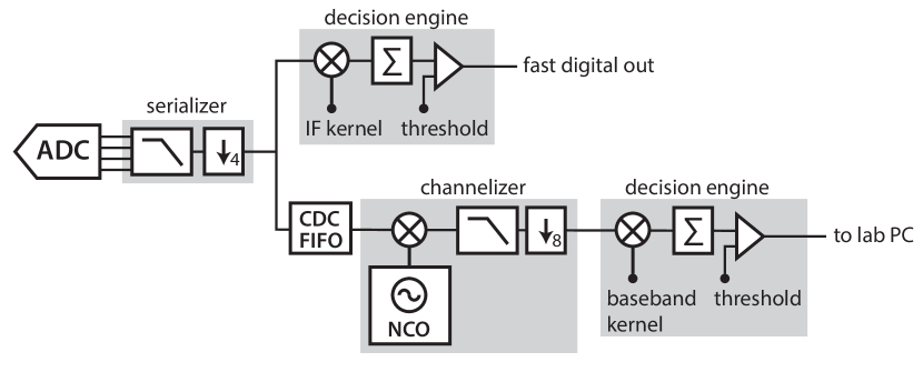
The raw ADC values from each ADC are presented to the FPGA four samples wide at 250 MHz when sampling at 1 GS/s (we sample at the maximum rate to minimize noise aliasing). We immediately decimate by a factor of 4 by summing the four values so that subsequent processing deals with only one sample per clock. This is mainly for convenience: the raw integrators could run in parallel and the data could be serialized for the subsequent filtering. The data is copied to IF kernel integrators for multiplexed readout. The outputs of these fast integrators are connected to variable thresholders which drive digital outs to make fast qubit state decisions available to the pulse sequencing hardware for feedback. These values are also available in software as complex values.
For more conventional downconversion, each raw stream is also broadcast to a channelizer module. The module consists of a numerically controlled oscillator (NCO) that generates cosine and sine at the chosen frequency. The incoming ADC data is multiplied with the NCO outputs in a complex multiplier. The mixed signal is then low-pass filtered by a two-stage decimating finite-impulse response (FIR) filter chain. Polyphase FIR filters are chosen for each stage to minimize use of specialized DSP hardware on the FPGA. The FIR filters are equiripple with the coefficients designed by the Remez exchange algorithm McClellan and Parks (1973). The number of taps was chosen to optimally fit onto the DSP blocks of the FPGA (with reuse from hardware oversampling) and to suppress the stopband by 60 dB, nearly down to the bit level of the 12-bit ADCs. The low-pass filtered and decimated stream is useful for observing and debugging the cavity response. Finally, a decision engine using a baseband kernel integrator is attached to the demodulated stream to complete the conventional DSP chain.
III Dynamic Arbitrary Pulse Sequencing: APS2
There are demanding requirements on bandwidth, latency and noise for dynamic pulse sequencing with superconducting qubits. The sequencer should naturally represent the quantum circuit being applied, i.e., it should be able to apply a sequence of pulses (typical single qubit gate times) rather than treating the entire sequence as a waveform. Simply concatenating waveforms together to create a sequence places extreme demands on the size of waveform memory, and transferring and compiling sequences to the AWG becomes an experimental bottleneck. The sequencer should be able to respond to real-time information from qubit measurement results to make dynamic sequence selection within some small fraction of the relaxation time of the qubits. Finally, the sequencer output should have sufficiently low noise not to limit gate fidelity.
Typical AWGs rely on a precalculated list of sequences played out in a predetermined manner, or at best, loops of segments with simple jump responses to an event trigger. Dynamic sequences that implement quantum algorithms require more sophisticated control flow with conditional logic and branching in response to measurement results. In addition to dynamic control flow, the sequencer should also support code reuse through function calls and looping constructs to keep memory requirements reasonable for long verification and validation experiments such as randomized benchmarking Knill et al. (2008) or gate set tomography Blume-Kohout et al. (2013).
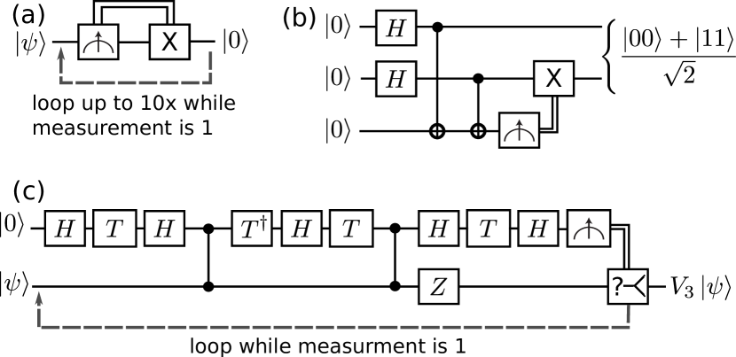
Figure 4 shows some elementary circuits that require fast feedback or feedforward. A simple and immediately useful primitive is the active reset of a qubit shown in Fig. 4(a). This can remove entropy from the system by refreshing ancilla qubits or simply improve the duty cycle of an experiment in comparison to waiting several multiples of for the qubit to relax to the ground state. With appropriate control flow instructions, reset with a maximum number of tries is naturally expressed as a looping construct with conditional branching for breaking out of the loop. Indeed the entire routine could be wrapped as a function call to be reused at the beginning of every sequence. Entanglement generation by measurement, shown in Fig. 4(b) is another useful primitive for resource state production that relies on feedforward. The circuit is also a useful testbench as it is very similar to the circuits for syndrome measurement in error correcting codes. Finally, Fig. 4(c) shows a more sophisticated use of feedforward. Implementing T gates will most likely dominate the run time of an error corrected quantum circuit Raussendorf, Harrington, and Goyal (2007). However, if the circuit can be probabilistic then the average T gate depth can be reduced. These “repeat-until-success” circuits Paetznick and Svore (2014) bring in one or more ancilla qubits and perform a series of gates and interactions. Then, conditional on the result of measuring the ancilla either the desired gate or a identity operation has been applied to the data qubit. In the identity case, the gate can be attempted again by repeating the circuit with a refreshed ancilla.
The APS2 was constructed to satisfy all these criteria by tailored design of the sequencer. The sequencing engine processes an instruction set that provides full arbitrary control flow and can play a new waveform every (two FPGA clock cycles) to naturally and compactly represent any superconducting qubit circuit with feedback or feedfoward. Realtime state information is fed in via high-speed serial links from the TDM. A cache controller intermediates access to deep memory for longer experiments. We now discuss in detail some of the design choices.
III.1 Arbitrary Control Flow
Arbitrary control flow can be fulfilled with three concepts: sequences, loops (repetition) and conditional execution. We add to this set the concept of subroutines because of their value in structured programming and memory re-use. The gateware implements a control unit state machine with four additional resources: a loadable incrementing program counter indicating the current address in instruction memory; a loadable decrementing repeat counter; a stack that holds the repeat and program counter values; and a comparison register that holds the last comparison boolean result. The specific instruction set supported is shown in Table 1.
| WAVEFORM | dispatch instruction to waveform engine(s) | \rdelim}325mm[output] |
|---|---|---|
| MARKER | dispatch instruction to marker engine(s) | |
| MODULATOR | dispatch instruction to I/Q modulator engine | |
| WAIT | broadcast wait command to all output engines | \rdelim}225mm[synchronization] |
| SYNC | wait until all execution engine queues are empty | |
| LOAD_REPEAT | load value into the repeat register | \rdelim}925mm[flow control] |
| REPEAT | if repeat register is 0 continue; otherwise decrement repeat register and jump to given address | |
| LOAD_CMP | load comparison register with next value in serial link FIFO | |
| CMP | compare given mask to comparison register with given binary comparison operation (, , , ) and store result in comparison result register | |
| GOTO | jump to given instruction address (optionally conditionally) | |
| CALL | push stack and jump to the given instruction address (optionally conditionally) | |
| RETURN | pop stack and return to the call site | |
| PREFETCH | prefetch an instruction cache line |
The WAVEFORM, MARKER and MODULATOR instructions enable analog and digital output and are immediately dispatched to output execution engines (see sections III.1.1 and III.1.2 below). The next two instructions, WAIT and SYNC, enable synchronization both between output engines on the same APS2 and between APS2 modules (see section III.1.1 below). The next set of instructions provides arbitrary control-flow: LOAD_REPEAT and REPEAT enable looping constructs; LOAD_CMP enables access to the real-time steering information fed from the TDM; CMP and GOTO enable conditional branching; CALL and RETURN allow for subroutines and recursion, enabling, for example, nested loops without multiple loop counters. Finally, although not directly related to control flow, PREFETCH gives hints to the cache controller to avoid cache misses.
III.1.1 Super-scalar Architecture
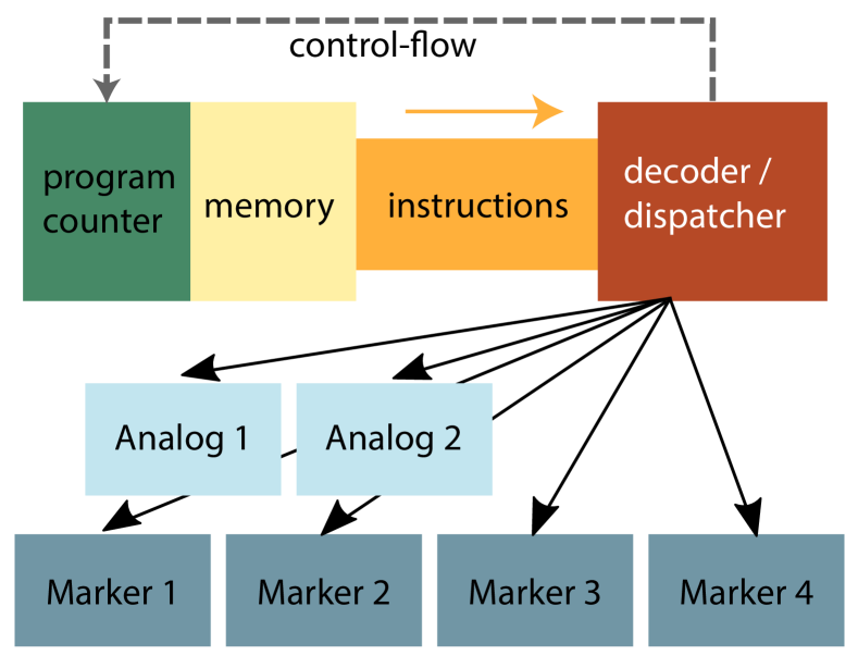
Each APS2 module has multiple outputs driven by individual execution engines: two analog channels and four marker channels. We use dispatch from a single instruction stream to simplify synchronization of control flow across multiple output engines (Fig. 5). Since each execution engine has its own internal FIFO buffer, this also allows the decoder/dispatcher to greedily look ahead and process instructions (contingent on deterministic control flow) and potentially dispatch to the execution units. The look ahead strategy absorbs the pipelining latency due to an instruction counter address jump after a CALL, RETURN or REPEAT instruction.
The superscalar approach has to accept some additional complexity in order to convert a serial instruction stream into potentially simultaneous operations in the execution engines. The APS2 provides two mechanisms to solve this synchronization task. The first mechanism is a WAIT instruction that stalls the execution engines until a trigger signal arrives. While the engines are stalled, the control flow unit/dispatcher continues to load instructions into the output engine buffers. The execution engines respond synchronously to trigger signals, so in this mechanism an external signal provides simultaneity and a method to synchronize multiple modules. The second mechanism, the SYNC instruction, acts as a fence or barrier to ensure that all execution engines are at the same point by stalling processing of instructions until all engines’ execution queues are empty. This is also useful for resynchronizing after a non-deterministic wait time - e.g. an uncertain delay before a measurement result is valid.
III.1.2 Output Engines
Each analog and digital output channel is sequenced by a waveform or marker “output engine” that takes a more limited set of instructions.
Waveform Engine
The waveform engines create analog waveforms from the following set of instructions:
-
1.
PLAY play a waveform starting at a given address for a given count;
-
2.
WAIT stall playback until a trigger arrives;
-
3.
SYNC stall until the main decoder indicates all engines are synchronized;
-
4.
PREFETCH fill a page of the waveform cache from deep memory - see section III.2.2 for further details.
Typically, each PLAY instruction corresponds to a pulse implementing a gate and so it is important that the waveform engine be fed and be able to process instructions on a timescale commensurate with superconducting qubit control pulses. The main decoder can dispatch a waveform instruction every and the waveform engine can jump to a new pulse every . In addition, typical pulse sequences contain idle periods of zero or constant output. Rather than inefficiently storing repeated values in waveform memory. Rather the instruction is “play this waveform value for samples” Morgan (1987). We refer to these as Time-Amplitude (TA) pairs and can mark any waveform command as such.
Marker Engine
Marker engines creates digital outputs from the following set of instructions:
-
1.
PLAY play marker with a given state for a given count;
-
2.
WAIT stall playback until a trigger arrives;
-
3.
SYNC stall until the main decoder indicates all engines are synchronized.
The natural sample rate for the marker PLAY commands are in terms of the sequencer FPGA clock which runs at a quarter of the analog output rate. To provide single sample resolution we route the marker outputs through dedicated serializer hardware (Xilinx OSERDESE2). For all but the last sample the 4 marker samples are simply copies of the desired output state. However, the last word is programmable as part of the PLAY instruction to provide full resolution of the marker rising/falling edge.
III.1.3 Modulation Engine
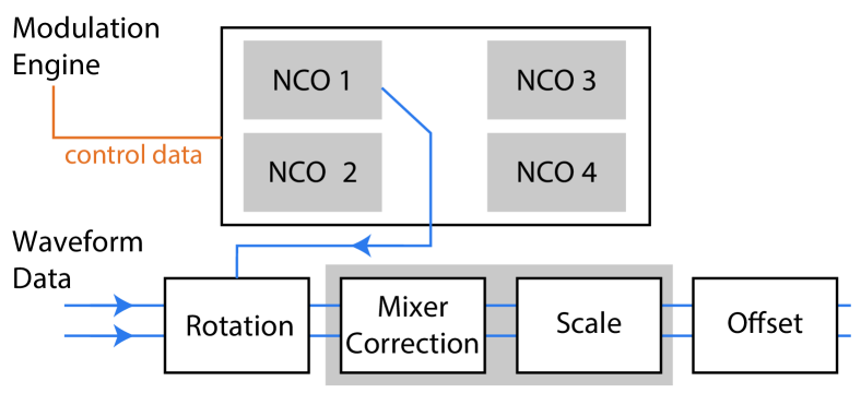
An APS2 module is typically used to drive the I and Q ports of an I/Q mixer to modulate the amplitude and phase of a microwave carrier, thus producing the control or readout signal. To improve the on/off ratio, the carrier is typically detuned from the qubit or cavity frequency and the I/Q waveforms modulated at the difference frequency with an appropriate phase shift to single-sideband (SSB) modulate the carrier up or down to the qubit/cavity frequency. Qubit control is defined in a rotating frame at the qubit frequency so the phase of the modulation has to track the detuning frequency. Z-rotations are implemented as frame updates that shift the phase of all subsequent pulses Knill et al. (2000). For deterministic sequences, the modulation and frame changes can be pre-calculated and stored as new waveforms in the pulse library. However, for conditional execution or for experiments with non-deterministic delays, this is not possible and the modulation and frame changes must be done in real-time.
To support both SSB modulation and dynamic frame updates, the APS2 includes a modulation engine which phase modulates the waveform output, and that can be controlled via sequence instructions. The modulation engine contains multiple NCOs to enable merging multiple “logical” channels at different frequencies onto the same physical channel pair. For example, to control two qubits, two NCOs can be set to the detuning frequencies of each qubit, and control pulses can be sent to either qubit with the appropriate NCO selection, while the hardware tracks the other qubit’s phase evolution. The phase applied to each pulse is the sum of the accumulated phase increment (for frequency detuning), a fixed phase offset (e.g. for setting an or pulse), and an accumulated frame (to implement -rotations). The modulation engine supports the following instructions
-
1.
WAIT stall until a trigger is received;
-
2.
SYNC stall until the main decoder indicates all engines are synchronized;
-
3.
RESET_PHASE reset the phase and frame of the selected NCO(s);
-
4.
SET_PHASE_OFFSET set the phase offset of the selected NCO(s);
-
5.
SET_PHASE_INCREMENT set the phase increment of the selected NCO(s);
-
6.
UPDATE_FRAME update the frame of the selected NCO(s);
-
7.
MODULATE select a NCO for a given number of samples.
All NCO phase commands are held until the the next instruction boundary, which is the end of the currently playing MODULATE command or a synchronization signal being received. The commands are held to allow them to occur with effectively no delay: for example, the phase should be reset when the trigger arrives; or a rotation should happen instantaneously between two pulses.
In addition, I/Q mixers have imperfections that can be compensated for by appropriate adjustments to the waveforms. In particular, carrier leakage may be minimized by adjusting DC offsets, and amplitude/phase imbalance compensated with a 2x2 correction matrix applied to the I/Q pairs. The APS2 includes correction matrix and offset blocks after the modulator to effect these adjustments, as shown in Fig. 6.
III.2 Caching Strategies
Some qubit experiments, e.g. calibration and characterization, require long sequences and/or many waveform variants. Supporting such sequences requires an AWG with deep memory. However, AWG sequencers immediately run into a well-known depth/speed trade-off for memory: SDRAM with many gigabytes of memory has random access times of 100s of nanoseconds whereas SRAM, or on-board FPGA block RAM, can have access times of only a few clock cycles but are typically limited to only a few megabytes. This memory dichotomy drives some of the sequencing characteristics of commercial AWGs. For example, the Tektronix 5014B requires to switch sequence segments and the Keysight M8190A requires a minimum sequence segment length of . These delay times are incompatible with the typical gate times of 10s of nanoseconds for superconducting qubits. However, it is possible to borrow from CPU design and hide this latency by adding instruction and waveform caches to the memory interface.
The APS2 has of DDR3 SDRAM to dynamically allocate to a combination of sequence instructions and waveforms. This corresponds to up to 128 million sequence instructions or 256 million complex waveform points, sufficient for most current experiments. The sequencer and waveform engines interface with this deep memory through a cache controller with access to FPGA block RAM. If the requested data is in the cache, then it can be returned deterministically within a few clock cycles, whereas if there is a cache miss the sequencer stalls while the data is fetched from SDRAM. Cache misses during a sequence are generally catastrophic given superconducting qubit coherence times. However, with heuristics and PREFETCH hints from the compiler, the cache controller can ensure data has been preloaded into the block RAM before it is requested and avoid any cache stalls.
III.2.1 Instruction Cache
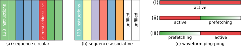
The APS2 instruction cache is split into two parts to support two different heuristics about how sequences advance through the instruction stream—see Fig. 7(a-b). We chose cache line sizes of 128 instructions or 1 kB, which is significantly larger than those used in a typical CPU (Intel/AMD processors typically have cache lines of only 64 bytes) but reflects the lack of a nested cache hierarchy and the more typical linear playback of quantum gate sequences. The first cache is a circular buffer centered around the current instruction address that supports the notion that the most likely direction is forward motion through the instructions, with potential local jumps to recently played addresses when looping. The controller greedily prefetches additional cache lines ahead of the current address but leaves a buffer of previously played cache lines for looping. Function calls, or subroutines, require random access so the second instruction cache is fully associative. The associative cache lines are filled in round-robin fashion with explicit PREFETCH instructions. This first-in-first-out replacement strategy for the associative cache ignores any information about cache line usage. Since the cache controller tracks access, a simple extension would be a Least Recently Used (LRU) or pseudo-LRU algorithm. It also places a significant burden on the compiler to insert the PREFETCH instructions and group subroutines into cache lines. However, given the severe penalty of a cache miss it is difficult to envisage a hardware-implemented cache controller that can alleviate that burden.
III.2.2 Waveform Cache
In use cases we have examined, waveform access does not have the nearly linear structure of sequence instructions. Rather, a sequence tends to require random access to a small library of short waveforms, where that library may change over time due to calibration or feedback signals, or the desire to scan a range of waveforms. The APS2 has a waveform cache of 128 ksamples to support fast access to a large waveform library. For scenarios demanding that the library change over time, the cache is split into two pages of 64 ksamples—see Fig. 7(c). The cache is composed of dual-port block RAM and so a sequence can be actively playing waveforms from one page while the second page is filled from SDRAM. The two pages’ roles can then alternate supporting total waveform library sizes up to the limit of the SDRAM. For this mode of operation we do not expect to change the waveform library within a single sequence. Filling an entire waveform cache page takes , meaning that at typical repetition rates of 10s of kHz we can exchange the waveform library every few sequences.
IV Synthesizing and Distributing Steering Information
As we move beyond simple single qubit feedback circuits we need to synthesize steering decisions from multiple qubit measurement results, and then communicate the steering decision to multiple sequencers. We have designed a dedicated hardware module, the Trigger Distribution Module (TDM), to take in up to eight qubit state decisions and send steering information to up to nine pulse sequencers—see Fig. 8 for a block diagram.
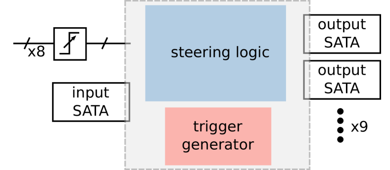
There are eight SMA inputs that feed variable comparators for reading in qubit measurement results from QDSP, with one input used as a data valid strobe. The TDM can communicate to all the APS2 modules in an enclosure via a high speed serial connection over SATA cables. The star distribution network also allows us to use the distribution module for synchronization. A reserved symbol acts as a trigger that can be broadcast to all APS2 modules in an enclosure for synchronous multi-module output. There is one additional SATA serial link that can be used for inter-crate communications with other TDM’s for for future larger circuits that cannot be controlled with a single crate.
The baseline TDM gateware APS2-TDM (github.com/BBN-Q/APS2-TDM) currently broadcasts the measurement results to all APS2 modules. As a result, every APS2 must allow a sequence branch for each result, even when the controlled qubit is not affected by that particular measurement. A more flexible decision logic and sequence steering will become critical in larger circuits. Since all measurement results flow through the TDM, it is natural to consider it orchestrating the entire experiment. For example, in error correction, syndrome decoding could be implemented by the TDM and the required qubit corrections sent to the relevant APS2s only. We see the TDM as a testbed for building out a more scalable qubit control platform with a hierarchy of controllers, where the TDM assumes the role of routing measurement results and steering the computation.
V Latency
With all the pieces in place we can examine the latency budget of a closed feedback loop and highlight potential areas for improvement. A detailed listing is provided in Table 2. The total latency from the end of a measurement pulse to the next conditional pulse coming out of the APS2 is . Our test setup incurs an additional of latency from cabling to/from the qubit device in the dilution refrigerator, as well as analog filtering. The total latency is comparable to 1% of the qubit relaxation time and our measurement time, and is not the limiting factor in our circuit implementation fidelities.
| Step | Latency (ns) |
|---|---|
| ADC capture | 32 |
| digital signal processing | 56 (14 clocks) |
| X6 to TDM interface | 10 (1 clock) |
| TDM distribution logic | 10 (1 clock) |
| TDM to APS2 module interface | 210 |
| APS2 address jump | 53 (16 clocks) |
| APS2 waveform signal processing | 30 (9 clocks) |
| DAC output | 29 |
| Total | 428 |
However, there are a few areas amenable to improvement. The APS2 design prioritized instruction throughput and waveform cache size. This required significant buffering and pipelining. Optimizing instead for latency could tradeoff those capabilities for reduced latency for an APS2 address jump. The serial link between the TDM and APS2 is slow due to FIFOs that manage data transfer through asynchronous clock domains. However, synchronizing the TDM and APS2 to a common reference creates a stable phase relationship between clocks domains which would allow these FIFOs to be removed and save . Modest benefit could be obtained by integrating the readout system into the TDM, saving two data transfer steps.
While not listed in the table, the delays from cabling and analog filtering are also non-negligible. Since we digitize data at 1GS/s, minimal analog low pass filtering after mixing down to the IF is necessary, except to prevent overloading amplifiers or the ADC. Moving the hardware physically closer to the top of the dilution refrigerator would save . The reduction in cable delays is one potential benefit to cyrogenic control systems, but is only a fraction of the total latency budget.
VI Feedback and feedforward in circuit QED
The integration of QDP systems and APS2/TDM modules into a circuit QED apparatus enables a variety of qubit experiments requiring feedback or feedforward. Feedback indicates that measurements modify control of the measured qubit, while in feedforward the conditional control acts on different qubits. Here we present some examples of simultaneous dynamic control of up to three qubits. We emphasize that the hardware system was designed for flexible multi-qubit experiments that allows for programming different experiments in software, with minimal or no hardware changes.
The quantum processor used here, first introduced in Ref. Ristè et al., 2017, is a five-qubit superconducting device housed in a dilution refrigerator at . The wiring inside the refrigerator is very similar to the reference above, with the exception of the addition of a Josephson parametric amplifier (JPA) Hatridge et al. (2011) to boost the readout fidelity of one qubit. The control flow of qubit instructions, previously a pre-orchestrated sequence of gates and measurements, is now steered in real time by a TDM. This module receives the digital qubit measurements from QDSP digital outputs, and distributes the relevant data to the APS2 units which then conditionally execute sequences.
VI.1 Fast qubit initialization
As a first test of our control hardware, we start with the simplest closed-loop feedback scheme — fast qubit reset Ristè et al. (2012); Campagne-Ibarcq et al. (2013). A reliable way to initialize qubit registers is one of the prerequisites for quantum computation DiVincenzo (2000). Conventionally, initialization of superconducting qubits is accomplished by passive thermalization of the qubit to the near zero-temperature environment. However, with a characteristic relaxation time (see Table 2 for relaxation time details), the necessary waiting constitutes the majority of the experiment wall clock time. Furthermore, passive initialization slows re-use of ancilla qubits during a computation, a feature that would relieve the need for a continuous stream of fresh qubits in a fault-tolerant system Ben Or, Gottesman, and Hassidim (2013).
Feedback-based reset aims to remove entropy on demand using measurement and a conditional bit-flip gate (Fig. 9 inset) Ristè et al. (2012). This operation ideally resets the qubit state to if the measurement result is , or leaves it unchanged if , giving an unconditional output state . The effect of reset is evident when considering the initialization success probability compared to no reset (passive initialization) (Fig. 9). As the initialization time is decreased to or lower, passive initialization becomes increasingly faulty, while active reset is largely unaffected.
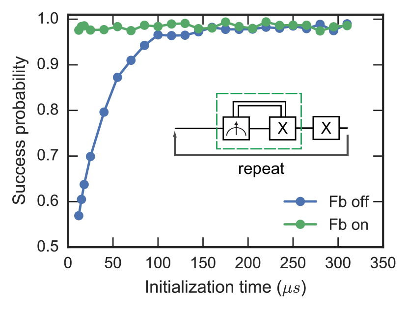
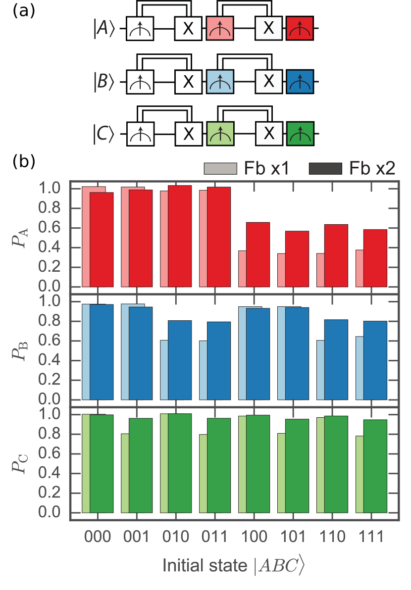
We extend this protocol to reset a register of three qubits simultaneously. This is accomplished with no additional hardware beyond that already required for the open-loop control of the same number of qubits. We exploit frequency multiplexing to combine two readout signals, so that all signal processing can be accomplished with the two analog inputs of a single X6-1000M. The control flow simply replicates the conditional bit-flip logic across the three qubits (Fig. 10a). We assess the performance of the three-qubit reset by measuring the success probabilities for resetting each individual qubit starting from the eight computational input states (Fig. 10b). The deviation in success probabilies is largely due to the difference in readout fidelities (Table 3), as only qubit is equipped with a JPA.
VI.2 Measurement-based and gates
Our hardware is also readily applicable to feedforward scenarios, where the result of a measurement conditions the control of different qubits. A first example is the realization of measurement-based gates. In an error-corrected circuit, gates on a logical qubit can be made fault-tolerant by applying them transversally to all the underlying physical qubits. However, for any given code, a universal gate set cannot all be implemented transversally Chen et al. (2008). For instance, in the surface code, all Pauli operations , , are transversal, but partial rotations such as are not. To fill this gap, fault-tolerant gates can be constructed with interactions with ancilla qubits and control conditioned on measurement results Bravyi and Kitaev (2005).
Here we demonstrate the basic principle of measurement-based gates, implementing partial rotations on a physical qubit, using an ancilla and feedforward operations. The initial state of the ancilla, which can be prepared offline to the computation, determines the rotation angle . Typical gates are denoted with () and (). An gate can be decomposed into an ancilla measurement and a conditional gate Bravyi and Kitaev (2005), which is transversal in the surface code (Fig. 11a). Starting with the ancilla in a superposition state, , the result of the ancilla measurement determines whether the final state approximates the desired (Fig. 11d), or the shifted (e). In the latter case, a corrective , applied as a frame update (see Sec. III.1.3), gives the intended state deterministically (f). The reduced coherence, indicated by the length of the arrow, is mainly due to the measurement time (), with the addition of decision latency in (f).
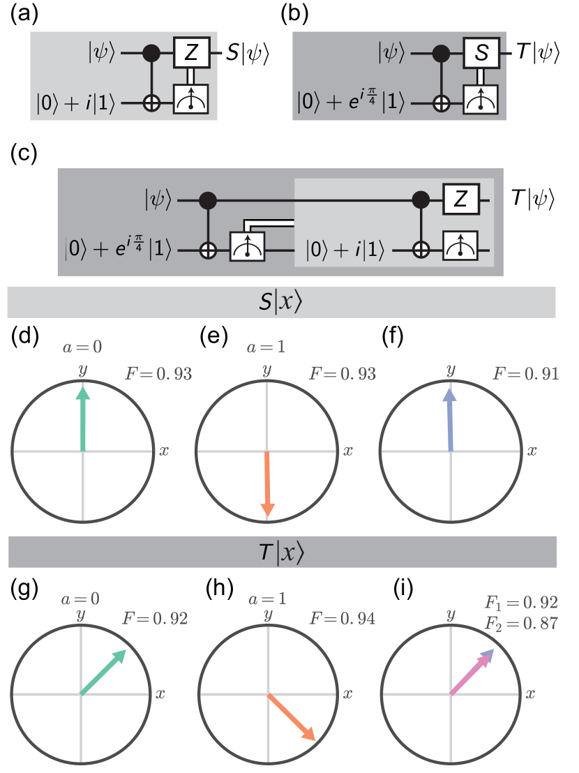
Similarly, a gate can be implemented with a different ancilla preparation and a conditional gate (Fig. 11b). However, as seen before, the gate cannot be applied transversally, so it is in turn decomposed into the feedforward sequence above. The result is a nested feedforward loop with up to two ancilla measurements and conditional sequences (Fig. 11c). We reuse the same ancilla in the second round, taking advantage of the first measurement to initialize it in a known state. By using the CLEAR protocol McClure et al. (2016), we reduce the latency before we can reuse the ancilla (Fig. 11g-i).
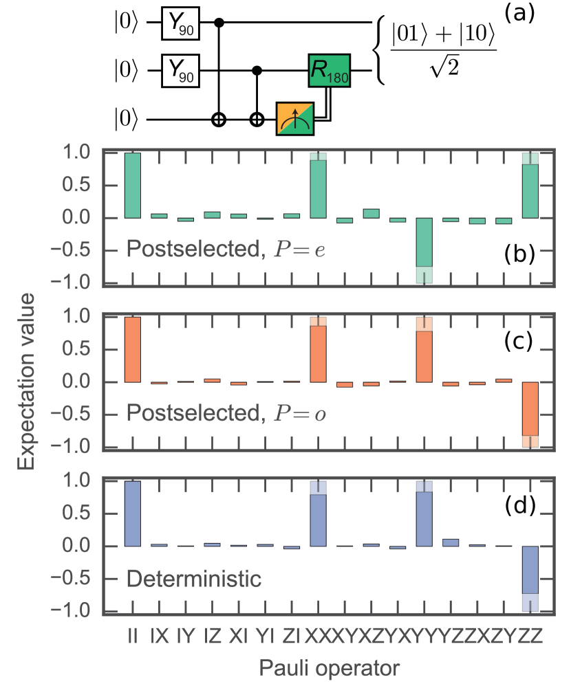
VI.3 Entanglement generation through measurement
With three qubits, feedforward control can be used to generate entanglement by measurement. Two qubits separately interact with a third ancilla qubit to implement a parity measurement of the first two qubits (Fig. 12a). With the first two qubits starting in an equal superposition state, the parity measurement projects them onto either an even or odd Bell state with the ancilla measurement result containing the information about which (Fig. 12b-c). This parity measurement scenario, with ancillas and feedforward, is also relevant for syndrome extraction in quantum error correction schemes Bravyi and Kitaev (1998); Mermin (2007) and has been experimentally demonstrated in post-selected formSaira et al. (2014); Chow et al. (2014). With our hardware we can go one step further, and deterministically create the odd state by converting the projected even state into an odd one by a conditional bit-flip on one of the data qubits (Fig. 12d). This deterministic protocol has also been realized in Ref. Ristè et al., 2013, but with the ancilla qubit replaced by a cavity mode.
VII Conclusion
The APS2 and QDSP platforms are a complete hardware solution for dynamic quantum computing systems. They achieve this with tailored gateware and hardware that enable flexible, low-latency manipulation, thus allowing users to program generic quantum circuits without hardware reconfiguration. We have proved this hardware in situ with a superconducting quantum processor, showing a variety of novel dynamic circuits utilizing feedback and feedforward. To further improve this platform we intend to integrate control and readout into a unified hardware system, investigate improvements to the APS2 analog output chain and generalize system synchronization.
Upconversion systems generically require a multitude of components and suffer from various mixer imperfections, leading to instability and a spectrum polluted by mixer product spurs. Future hardware revisions may solve these issues by moving to faster RF DACs that can directly generate microwave tones with a cleaner spectrum Glascott-Jones et al. (2014). Direct RF output allows for greater frequency agility, allowing for channel re-use for both control and measurement. New DACs with sampling rates from 4–6 support output modes that direct power into higher Nyquist zones, removing pressure for ultra-high clock speeds. Future FPGAs may include many on-chip RF DACs Erdmann et al. (2017), potentially drastically increasing channel densities in control systems.
The typical way to achieve system synchronization is by building trigger fanout trees. This strategy becomes increasingly cumbersome and fragile as system sizes grow. A more scalable approach consists of sharing frequency and time between all devices, so that all modules in the system have a synchronous copy of a global counter. To achieve this, future hardware revisions may incorporate a time distribution protocol such as White Rabbit Serrano et al. (2009). Sharing time changes the synchronization paradigm from “go on trigger” to “go at time ”.
Finally, we are exploring methods to combine real-time computation with dynamic control-flow on the individual APSs. For example, a controller of a system of logical qubits must combine information from a logical decoder with program control-flow. A softcore CPU running on the TDM would enable rapid development of realtime infrastructure.
Acknowledgements.
Schematic capture and PC board layout for the APS2 and TDM were done by Ray Zeller and Chris Johnson of ZRL Inc., Bristol, RI. Nick Materise developed an initial prototype of the QDSP system in VHDL. This was converted into a Simulink model and tested with MATLAB HDL Coder before finally being converted back into pure VHDL. The data analysis for the experimental section was performed using code written in Julia Bezanson et al. (2014), and the figures were made with Seaborn Waskom et al. (2016) and matplotlib Hunter (2007). We used Scipy Jones et al. (01) to construct the filter coefficients for the QDSP system. The authors would like to thank George A. Keefe and Mary B. Rothwell for device fabrication, and Nissim Ofek for discussions about AWG instruction sets. This research was funded by the Office of the Director of National Intelligence (ODNI), Intelligence Advanced Research Projects Activity (IARPA), through the Army Research Office contract No. W911NF-10-1-0324 and No. W911NF-14-1-0114. All statements of fact, opinion or conclusions contained herein are those of the authors and should not be construed as representing the official views or policies of IARPA, the ODNI, or the U.S. Government.References
- Chow et al. (2014) J. M. Chow, J. M. Gambetta, E. Magesan, D. W. Abraham, A. W. Cross, B. R. Johnson, N. A. Masluk, C. A. Ryan, J. A. Smolin, S. J. Srinivasan, and M. Steffen, “Implementing a strand of a scalable fault-tolerant quantum computing fabric.” Nature Communications 5, 4015 (2014).
- Steffen et al. (2013) L. Steffen, Y. Salathe, M. Oppliger, P. Kurpiers, M. Baur, C. Lang, C. Eichler, G. Puebla-Hellmann, A. Fedorov, and A. Wallraff, “Deterministic quantum teleportation with feed-forward in a solid state system,” Nature 500, 319–322 (2013).
- Ristè et al. (2013) D. Ristè, M. Dukalski, C. A. Watson, G. de Lange, M. J. Tiggelman, Y. M. Blanter, K. W. Lehnert, R. N. Schouten, and L. DiCarlo, “Deterministic entanglement of superconducting qubits by parity measurement and feedback,” Nature 502, 350–354 (2013).
- Gottesman (2009) D. Gottesman, “An Introduction to Quantum Error Correction and Fault-Tolerant Quantum Computation,” arXiv (2009), arXiv:0904.2557 .
- Aharonov et al. (1996) D. Aharonov, M. Ben-Or, R. Impagliazzo, and N. Nisan, “Limitations of Noisy Reversible Computation,” arXiv (1996), arXiv:9611028 [quant-ph] .
- Bravyi and Kitaev (2005) S. Bravyi and A. Kitaev, “Universal quantum computation with ideal Clifford gates and noisy ancillas,” Physical Review A 71, 022316 (2005).
- Knill (2005) E. Knill, “Quantum computing with realistically noisy devices,” Nature 434, 39–44 (2005).
- Paetznick and Svore (2014) A. Paetznick and K. M. Svore, “Repeat-until-success: Non-deterministic decomposition of single-qubit unitaries,” Quantum Info. Comput. 14, 1277–1301 (2014).
- Ristè et al. (2012) D. Ristè, C. C. Bultink, K. W. Lehnert, and L. DiCarlo, “Feedback control of a solid-state qubit using high-fidelity projective measurement,” Phys. Rev. Lett. 109, 240502 (2012).
- Campagne-Ibarcq et al. (2013) P. Campagne-Ibarcq, E. Flurin, N. Roch, D. Darson, P. Morfin, M. Mirrahimi, M. H. Devoret, F. Mallet, and B. Huard, “Persistent control of a superconducting qubit by stroboscopic measurement feedback,” Physical Review X 3, 021008 (2013).
- Pfa (2014) “Unconditional quantum teleportation between distant solid-state quantum bits,” Science 345, 532–535 (2014).
- Ofek et al. (2016) N. Ofek, A. Petrenko, R. Heeres, P. Reinhold, Z. Leghtas, B. Vlastakis, Y. Liu, L. Frunzio, S. M. Girvin, L. Jiang, M. Mirrahimi, M. H. Devoret, and R. J. Schoelkopf, “Extending the lifetime of a quantum bit with error correction in superconducting circuits,” Nature 536, 441–445 (2016), letter.
- Raussendorf and Harrington (2007) R. Raussendorf and J. Harrington, “Fault-tolerant quantum computation with high threshold in two dimensions,” Physical Review Letters 98, 1–4 (2007), arXiv:0610082 [quant-ph] .
- Schuster (2007) D. Schuster, PhD Thesis, Ph.D. thesis, Yale University (2007).
- Bourdeauducq et al. (2016) S. Bourdeauducq, R. Jördens, P. Zotov, J. Britton, D. Slichter, D. Leibrandt, D. Allcock, A. Hankin, F. Kermarrec, Y. Sionneau, R. Srinivas, T. R. Tan, and J. Bohnet, “Artiq 1.0,” (2016).
- Chen et al. (2012) Y. Chen, D. Sank, P. O’Malley, T. White, R. Barends, B. Chiaro, J. Kelly, E. Lucero, M. Mariantoni, A. Megrant, C. Neill, A. Vainsencher, J. Wenner, Y. Yin, A. N. Cleland, and J. M. Martinis, “Multiplexed dispersive readout of superconducting phase qubits,” Applied Physics Letters 101, 182601 (2012), http://dx.doi.org/10.1063/1.4764940 .
- Jeffrey et al. (2014) E. Jeffrey, D. Sank, J. Y. Mutus, T. C. White, J. Kelly, R. Barends, Y. Chen, Z. Chen, B. Chiaro, A. Dunsworth, A. Megrant, P. J. J. O’Malley, C. Neill, P. Roushan, A. Vainsencher, J. Wenner, A. N. Cleland, and J. M. Martinis, “Fast accurate state measurement with superconducting qubits,” Phys. Rev. Lett. 112, 190504 (2014).
- Bultink et al. (2016) C. C. Bultink, M. A. Rol, T. E. O’Brien, X. Fu, B. C. S. Dikken, C. Dickel, R. F. L. Vermeulen, J. C. de Sterke, A. Bruno, R. N. Schouten, and L. DiCarlo, “Active resonator reset in the nonlinear dispersive regime of circuit qed,” Phys. Rev. Applied 6, 034008 (2016).
- Homulle et al. (2016) H. Homulle, S. Visser, B. Patra, G. Ferrari, E. Prati, F. Sebastiano, and E. Charbon, “A Reconfigurable Cryogenic Platform for the Classical Control of Scalable Quantum Computers,” arXiv.org (2016), 1602.05786v1 .
- Conway Lamb et al. (2016) I. D. Conway Lamb, J. I. Colless, J. M. Hornibrook, S. J. Pauka, S. J. Waddy, M. K. Frechtling, and D. J. Reilly, “A FPGA-based instrumentation platform for use at deep cryogenic temperatures,” Review of Scientific Instruments 87, 1–8 (2016), arXiv:1509.06809 .
- Gambetta et al. (2007) J. Gambetta, W. Braff, A. Wallraff, S. Girvin, and R. Schoelkopf, “Protocols for optimal readout of qubits using a continuous quantum nondemolition measurement,” Physical Review A 76, 012325 (2007).
- Ryan et al. (2015) C. A. Ryan, B. R. Johnson, J. M. Gambetta, J. M. Chow, M. P. da Silva, O. E. Dial, and T. A. Ohki, “Tomography via correlation of noisy measurement records,” Physical Review A 91, 022118 (2015), arXiv:1310.6448 .
- McClellan and Parks (1973) J. McClellan and T. Parks, “A unified approach to the design of optimum FIR linear-phase digital filters,” Circuit Theory, IEEE Transactions on 20, 697–701 (1973).
- Knill et al. (2008) E. Knill, D. Leibfried, R. Reichle, J. Britton, R. B. Blakestad, J. D. Jost, C. Langer, R. Ozeri, S. Seidelin, and D. J. Wineland, “Randomized benchmarking of quantum gates,” Physical Review A (Atomic, Molecular, and Optical Physics) 77, 12307 (2008).
- Blume-Kohout et al. (2013) R. Blume-Kohout, J. K. Gamble, E. Nielsen, J. Mizrahi, J. D. Sterk, and P. Maunz, “Robust, self-consistent, closed-form tomography of quantum logic gates on a trapped ion qubit,” 87185, 12 (2013), arXiv:1310.4492 .
- Raussendorf, Harrington, and Goyal (2007) R. Raussendorf, J. Harrington, and K. Goyal, “Topological fault-tolerance in cluster state quantum computation,” New Journal of Physics 9 (2007), 10.1088/1367-2630/9/6/199, arXiv:0703143 [quant-ph] .
- Morgan (1987) D. E. Morgan, “Test signal generator,” (1987).
- Knill et al. (2000) E. Knill, R. Laflamme, R. Martinez, and C. Tseng, “An algorithmic benchmark for quantum information processing,” Nature 404, 368–370 (2000).
- Ristè et al. (2017) D. Ristè, M. P. da Silva, C. A. Ryan, A. W. Cross, A. D. Córcoles, J. A. Smolin, J. M. Gambetta, J. M. Chow, and B. R. Johnson, “Demonstration of quantum advantage in machine learning,” npj Quantum Information 3, 16 (2017), arXiv:1512.06069 .
- Hatridge et al. (2011) M. Hatridge, R. Vijay, D. Slichter, J. Clarke, and I. Siddiqi, “Dispersive magnetometry with a quantum limited SQUID parametric amplifier,” Physical Review B 83, 134501 (2011).
- DiVincenzo (2000) D. P. DiVincenzo, “The physical implementation of quantum computation,” Fortschritte der Physik 48, 771–783 (2000).
- Ben Or, Gottesman, and Hassidim (2013) M. Ben Or, D. Gottesman, and A. Hassidim, “Quantum Refridgerator,” arXiv (2013), arXiv:arXiv:1301.1995v1 .
- Chen et al. (2008) X. Chen, H. Chung, A. W. Cross, B. Zeng, and I. L. Chuang, “Subsystem stabilizer codes cannot have a universal set of transversal gates for even one encoded qudit,” Phys. Rev. A 78, 012353 (2008).
- McClure et al. (2016) D. T. McClure, H. Paik, L. S. Bishop, M. Steffen, J. M. Chow, and J. M. Gambetta, “Rapid driven reset of a qubit readout resonator,” Phys. Rev. Applied 5, 011001 (2016).
- Bravyi and Kitaev (1998) S. B. Bravyi and A. Y. Kitaev, “Quantum codes on a lattice with boundary,” arXiv:quant-ph/9811052 (1998).
- Mermin (2007) D. Mermin, Quantum Computer Science: An Introduction, 1st ed. (Cambridge University Press, 2007).
- Saira et al. (2014) O.-P. Saira, J. P. Groen, J. Cramer, M. Meretska, G. de Lange, and L. DiCarlo, “Entanglement genesis by ancilla-based parity measurement in 2D circuit QED,” Phys. Rev. Lett. 112, 070502 (2014).
- Glascott-Jones et al. (2014) A. Glascott-Jones, N. Chantier, F. Bore, M. Wingender, M. Stackler, J. Amblard, E. Bouin, V. Monier, M. Martin, and G. Jestin, “Direct conversion to X band using a 4.5 GSps SiGe Digital to Analog Converter,” in 2014 International Radar Conference (IEEE, 2014) pp. 1–6.
- Erdmann et al. (2017) C. Erdmann, E. Cullen, D. Brouard, R. Pelliconi, B. Verbruggen, J. Mcgrath, D. Collins, M. De La Torre, P. Gay, P. Lynch, P. Lim, A. Collins, and B. Farley, “16.3 A 330mW 14b 6.8GS/s dual-mode RF DAC in 16nm FinFET achieving −70.8dBc ACPR in a 20MHz channel at 5.2GHz,” in 2017 IEEE International Solid-State Circuits Conference (ISSCC) (IEEE, 2017) pp. 280–281.
- Serrano et al. (2009) J. Serrano, P. Alvarez, M. Cattin, E. G. Cota, J. Lewis, P. Moreira, T. Wlostowski, G. Gaderer, P. Loschmidt, J. Dedic, Cosylab, R. B r, T. Fleck, M.Kreider, C. Prados, and S. Rauch, “The White Rabbit Project,” in International Conference on Accelerator and Large Experimental Physics Control System (2009).
- Bezanson et al. (2014) J. Bezanson, A. Edelman, S. Karpinski, and V. B. Shah, “Julia: A Fresh Approach to Numerical Computing,” (2014), arXiv:1411.1607 .
- Waskom et al. (2016) M. Waskom, O. Botvinnik, drewokane, P. Hobson, David, Y. Halchenko, S. Lukauskas, J. B. Cole, J. Warmenhoven, J. de Ruiter, S. Hoyer, J. Vanderplas, S. Villalba, G. Kunter, E. Quintero, M. Martin, A. Miles, K. Meyer, T. Augspurger, T. Yarkoni, P. Bachant, M. Williams, C. Evans, C. Fitzgerald, Brian, D. Wehner, G. Hitz, E. Ziegler, A. Qalieh, and A. Lee, “seaborn: v0.7.1 (june 2016),” (2016).
- Hunter (2007) J. D. Hunter, “Matplotlib: A 2D graphics environment,” Computing in Science and Engineering 9, 99–104 (2007).
- Jones et al. (01 ) E. Jones, T. Oliphant, P. Peterson, et al., “SciPy: Open source scientific tools for Python,” (2001–), [Online; accessed 2016-01-14].