Tailoring the SiC surface - a morphology study on the epitaxial growth of graphene and its buffer layer
Abstract
We investigate the growth of the graphene buffer layer and the involved step bunching behavior of the silicon carbide substrate surface using atomic force microscopy. The formation of local buffer layer domains are identified to be the origin of undesirably high step edges in excellent agreement with the predictions of a general model of step dynamics. The applied polymer-assisted sublimation growth method demonstrates that the key principle to suppress this behavior is the uniform nucleation of the buffer layer. In this way, the silicon carbide surface is stabilized such that ultra-flat surfaces can be conserved during graphene growth on a large variety of silicon carbide substrate surfaces. The analysis of the experimental results describes different growth modes which extend the current understanding of epitaxial graphene growth by emphasizing the importance of buffer layer nucleation and critical mass transport processes.
-
July 2017
-
Keywords: epitaxial graphene, buffer layer growth, polymer-assisted, giant step bunching, hydrogen etching
Introduction
Clean crystal surfaces at high temperatures reveal characteristics that may be described by “annealing”, “etching” and “growth” [1, 2, 3, 4]. In the case of the two-component crystal SiC, these mechanisms may coincide since here the partial pressures of silicon and carbon-containing vapor species need to be considered separately to describe the equilibrium conditions at the surface. Especially below temperatures of the low vapor pressure of carbon-containing species compared to that of silicon species is the reason why, for example, thermal etching of the terrace edges may be accompanied by the growth of carbon domains [5, 6, 7]. In the case of annealing, thermally activated species reorganize on the surface without ultimately leaving the surface and enable the formation of an energetically preferred configuration [3]. In the case of clean SiC (0001) surfaces at temperatures of about in an argon atmosphere, this restructuring process leads to the formation of new surface steps but also to the formation of carbon domains due to preferred silicon desorption [8, 7]. The first carbon layer is the so-called buffer layer that saturates about of the dangling silicon bonds of the underlying substrate surface forming the R30 reconstruction [9, 10]. Depending on the process parameters and substrate properties, these morphological changes are often accompanied by the formation of terrace structures with heights of several nanometers, so-called giant steps. Especially substrates with a larger miscut angle () or those that were initially hydrogen-etched are known to support giant step bunching [11, 12]. Graphene formation across giant steps is typically described by step flow growth leading to the formation of monolayer domains on the terraces but also to continuous multilayer domains along the edges [7]. Most of the published experiments on epitaxial graphene growth, solely focus on the development of the graphene layer presuming a SiC surface that is already reconstructed by a buffer layer to explain their proposed models [13, 7, 14, 15]. However, this cannot adequately describe the dependency of giant step formation on process parameters such as the pressure of the ambient inert gas, heating rate, temperature and the properties of the starting surface [16, 17]. Some recent studies show that substrates may be processed such that low steps (e.g. ) are conserved by employing substrates with a small miscut angle (), by suitable annealing sequences or by polymer deposition for improved buffer layer growth [12, 17, 8, 18].
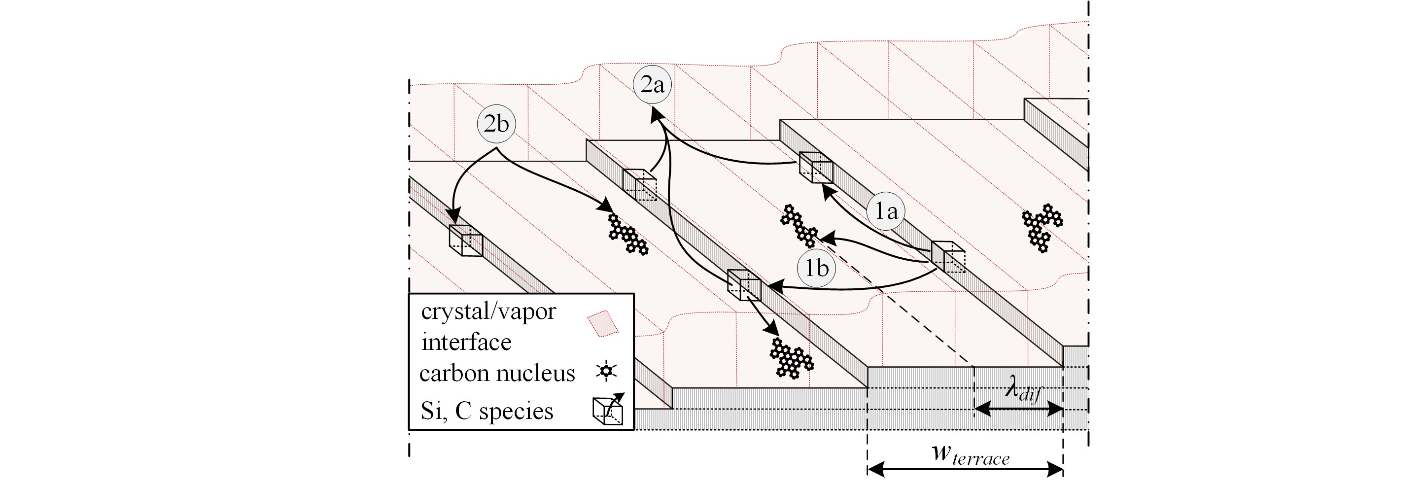
While the driving force of faceting of 6H-SiC is known to increase as a function of the miscut angle [19, 20], understanding the reasons for step bunching during epitaxial graphene growth requires further analysis of the role of carbon layers and the involved mass transport mechanisms. The present work focuses on the morphological changes that occur during the restructuring process of the surface to identify critical aspects which determine the quality of the final graphene sample. Figure 1 shows typical mass transport mechanisms at the interface of the SiC crystal surface during the initial stage of surface restructuring and buffer layer formation. Following the descriptions in literature, the equilibrium conditions at the surface are typically described by local reservoirs and sinks leading to growth and etching [21, 22, 23, 24]. Here, step edges, as well as the vapor/crystal interface, are assigned as silicon and carbon reservoirs while nuclei and the ambient atmosphere may represent sinks. The basic idea of the model is to differentiate between local mass transport processes by surface diffusion (1a, 1b) and so-called global mass transport processes via desorption and adsorption of silicon and carbon species through the vapor phase (2a, 2b). For epitaxial graphene growth, these mechanisms are often manipulated by affecting the mean free path length and partial pressures at the crystal/vapor interface using an inert argon gas atmosphere [25, 17] or by confinement control [26, 27]. The red shade layer in Figure 1 represents the Knudsen layer which is the highly non-equilibrium interface region in which direct interactions between gas molecules and the surface dominate [28, 29]. In the case of argon pressure, the thickness of the Knudsen layer is estimated to be a few hundred nanometers [29]. The partial pressures of mostly Si and small quantities of Si2C and SiC2 species forming above the SiC surface at temperatures below are known to significantly shift the growth temperature of the buffer layer and graphene towards higher values [6, 5]. The morphology study presented in this work identifies decisive mass transport and nucleation mechanisms that determine the step bunching behavior as well as the uniformity of the epitaxially grown carbon layers.
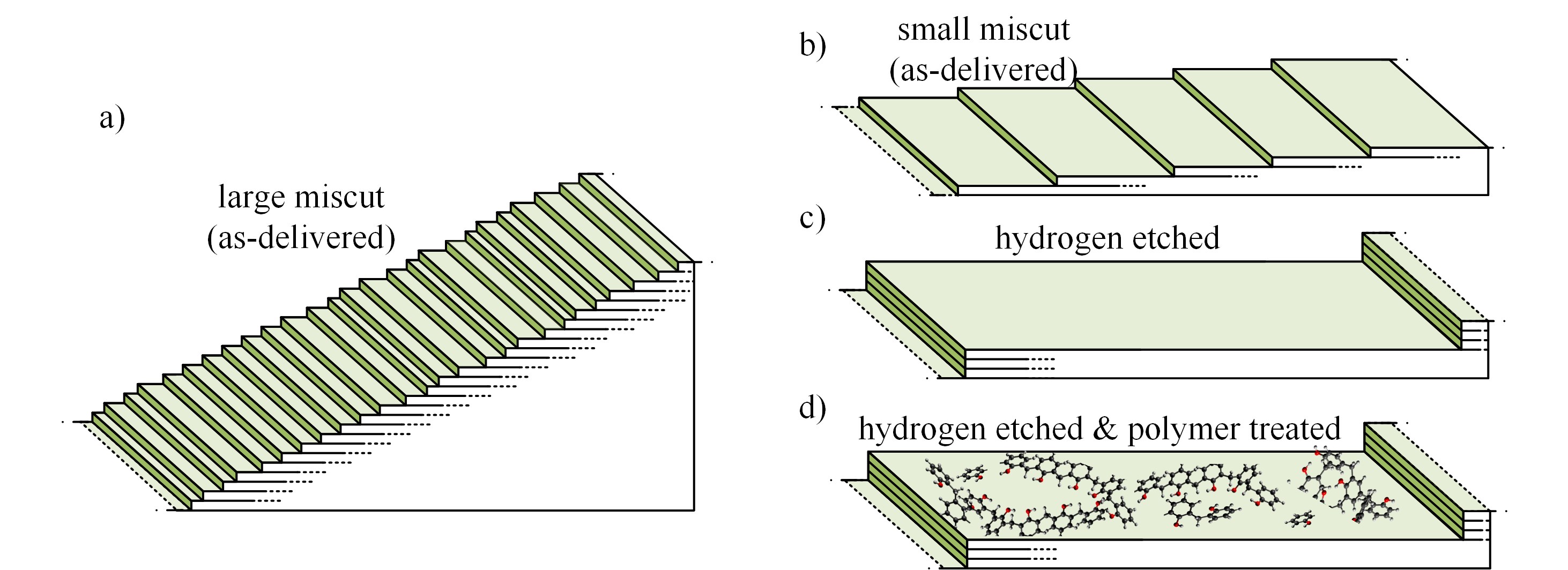
The first two sets of experiments (Figure 2(a-b)) focus on the influence of the substrate miscut angles. Both surfaces are “as-delivered” with terrace structures of single SiC bilayers and corresponding step heights of . The third set of experiments applies a “hydrogen-etched” surface (Figure 2(c)) with predefined steps and terraces having regular heights of which is a stable configuration of the SiC surface for the applied process parameters. In the last set of experiments (Figure 2(d)) hydrogen-etched substrates are treated with a polymer to investigate the impact of an additional carbon source on the growth behavior.
Sample preparation
The substrates were cut from semi-insulating epi-ready 6H-SiC () wafers. The two wafers had different miscut angles of (small-miscut) and (large-miscut) with respect to the (0001) crystal plane. The substrates used in the experiments presented in Figure 6-9 were initially prepared by hydrogen etching at temperatures of and . Etching of the Si-face at leads to step heights of and . This is only slightly higher compared to the step height of "as-delivered" surfaces (Figure 5(a)) and a noticeable improvement compared to the steps that are typically obtained by the standard etching procedure at (Figure 6(a)). After etching, the samples were applied to post-annealing at for at least to desorb adsorbed hydrogen from the SiC substrate which is accompanied by a further restructuring of the surface as shown in Figure 9(a). Additional information about hydrogen etching and post-annealing is given in the supplementary information. Polymer-assisted sublimation growth (PASG) was applied to support uniform buffer layer nucleation [18]. The deposition of polymer adsorbates was realized by liquid phase deposition (LPD) of AZ5214E photoresist (see ref. [18]). To control the size distribution of the adsorbate with heights shown in Figure 7(a) the sample was purged in an ultrasonic bath of isopropanol. The higher adsorbate density used for the experiment given in Figure 7(c) was realized by applying the procedure for the moderate density in the first step as well as by spin-coating of a weak solution of AZ5214E photoresist (, 4 droplets from the pipet solved in isopropanol) in the second step. The samples were introduced into the inductively heated hot-wall reactor which is typically evacuated to a base pressure of before starting the process. The buffer layer samples were processed by annealing at in argon at atmospheric pressure. To initiate graphene growth the temperature was further increased to for 6 minutes.
Giant step bunching induced by the buffer layer reconstruction
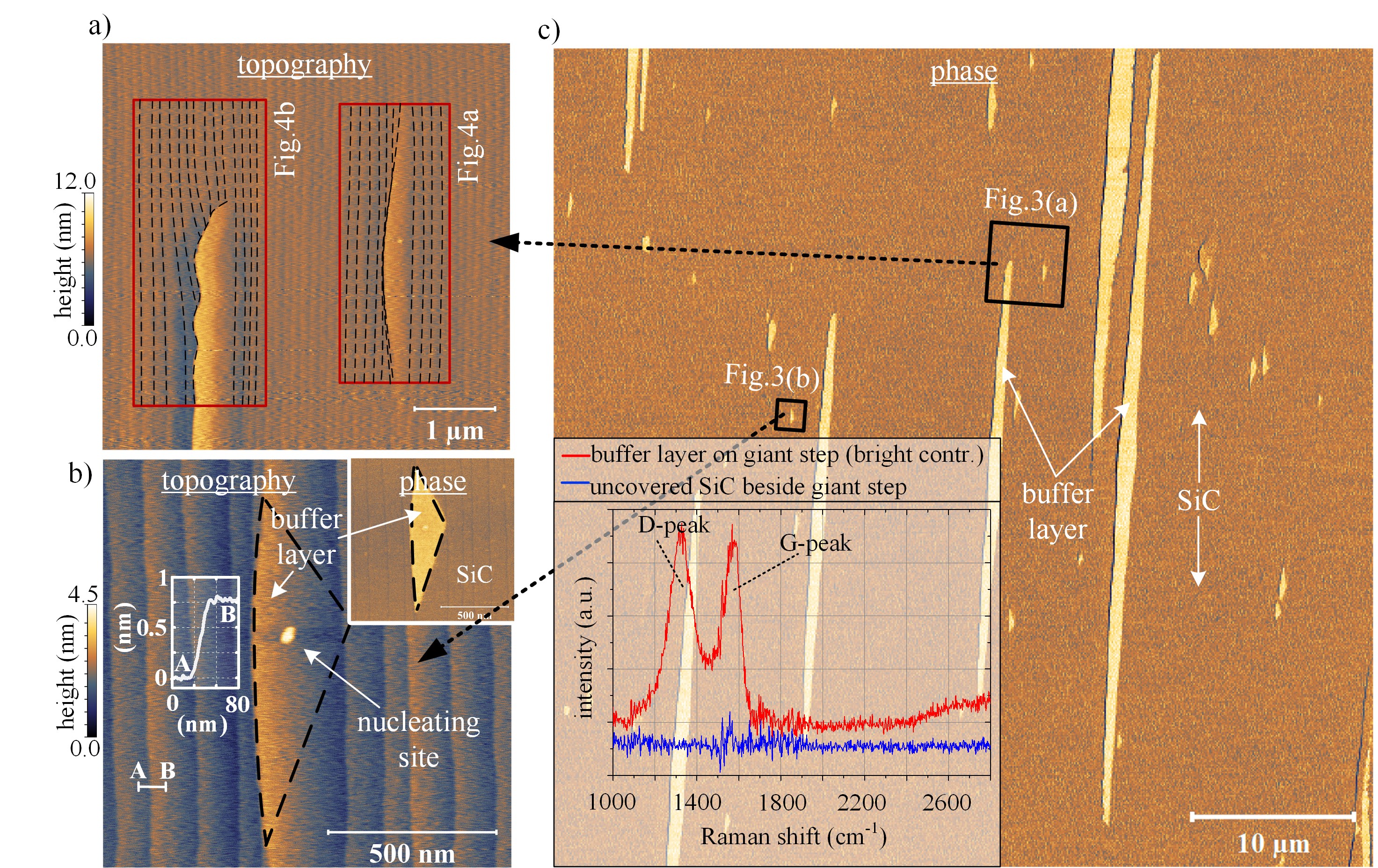
In the first experiment; the beginning of giant step formation on the SiC surface during high-temperature annealing (, ) in 1 bar argon atmosphere is studied on as-delivered substrates with a relatively large miscut angle as sketched in Figure 2(a). The atomic force microscopy (AFM) images in Figure 3 show three different kinds of terraces. In the magnified topographic images in Figure 3(a-b) one can identify narrow-stepped regions corresponding to terraces with a width of and a height of (see profile in Figure 3(b)) surrounding giant steps of different shapes. While the configuration of the narrow steps corresponding to repeated bunches of three SiC crystal layers is stable during the initial phase of the restructuring, also giant step formation is observed at some sites. The larger terraces are up to high, a few micrometers wide and several tens of micrometers long. Less developed giant steps such as those shown in Figure 3(b) are a few micrometers long and less than wide. Here, the step formation seems to be connected to a particle-like topographic signal in the center. This situation with terraces at different development stages is the beginning of completely giant stepped surfaces as it is observed after graphene growth, Figure 9(b). The AFM phase contrast in the inset of Figure 3(b) and in Figure 3(c) indicates a clear correlation between the light contrast and giant step formation while the darker contrast corresponds to regions with narrow steps. Raman measurements at such sites were performed with a spot size smaller to identify the reason for the distinctive signals. The two Raman spectra in the inset of Figure 3(c) are difference spectra which were obtained by subtracting the spectrum of an unprocessed SiC reference sample. The measurements reveal the characteristic signal of the buffer layer on broad terraces (red spectrum) while narrow stepped terrace regions show no Raman signal (blue spectrum) other than that of clean SiC. This surface condition describes the initiation of giant step bunching at and demonstrates that uncovered narrow steps become unstable once local buffer layer nucleation occurs.
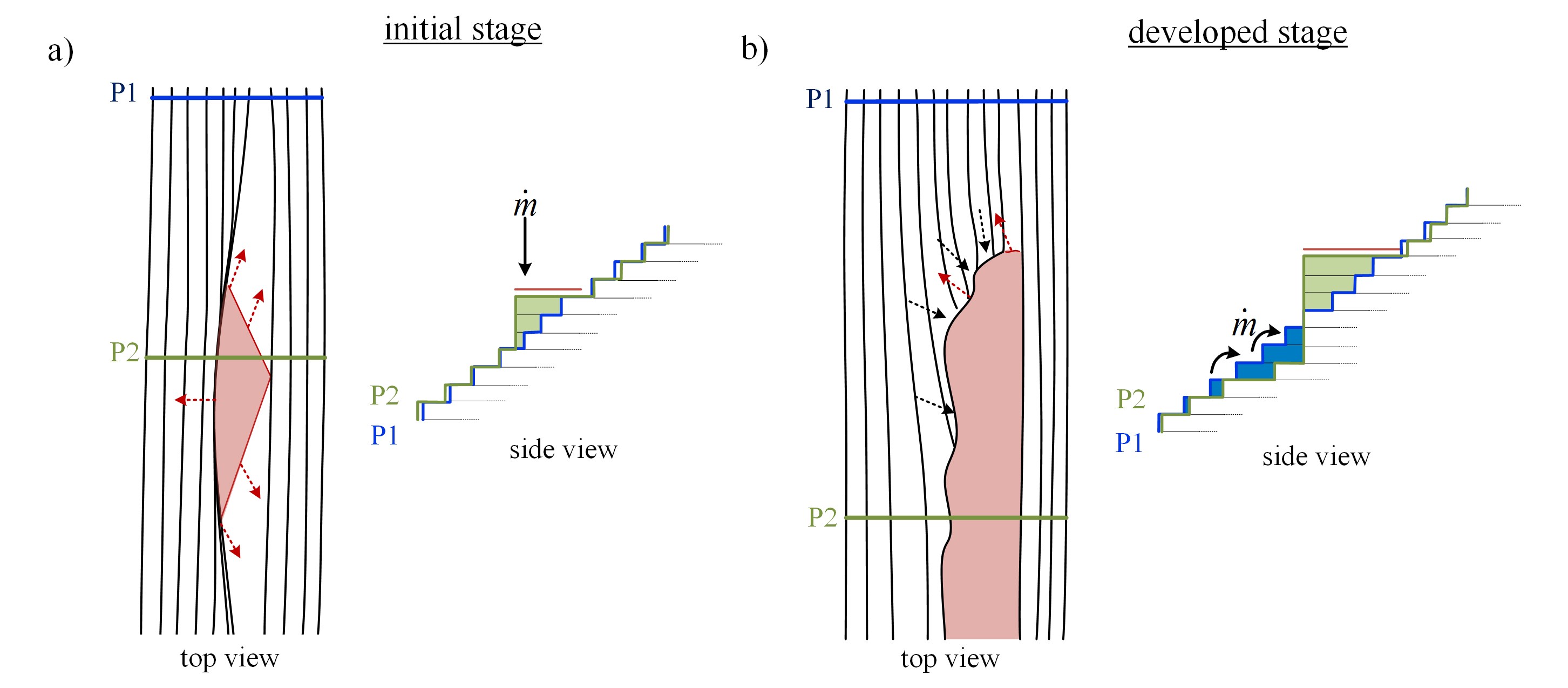
This behavior is explained by the general model developed by Jeong and Weeks. It states that the energetically favorable state of a new surface reconstruction is an important driving mechanism for step enlargement [22, 23, 30]. Our experimental results show that in the case of the SiC surface this reconstruction is represented by the buffer layer. Figure 4 depicts the top view of representative terraces and the corresponding side view of the step profiles created from the profile lines P1 (across narrow steps) and P2 (across the giant step). The drawings are derived from AFM measurements marked in Figure 3(a). The depicted terrace regions covered by buffer layer (red shade area) visualize the correlation between the locally formed buffer layer and step enlargement. The process of giant step bunching can be divided into two stages: the initial phase of step nucleation (Figure 4(a)) and the developed phase of continued growth of giant steps (Figure 4(b)). Despite the long annealing time of , many of the evolving broader terraces did not reach the stage of fully developed giant steps which suggests that the mechanisms in the initial growth stage are relatively slow. Regarding the model of Jeong and Weeks, this is typically the case as long as the width of a terrace is insufficiently wide to create a so-called “critical nucleus” [22, 23, 30]. On the SiC surface, one needs to distinguish between (i) a growing buffer layer domain that slowly enforce a widening of the terrace in the first stage (Figure 4(a)) and (ii) in the second stage the relatively fast growing giant steps when the critical width is reached (Figure 4(b)). Both processes (buffer layer and giant step formation) have their individual critical nucleus size. Critical nuclei for forming local buffer layer domains (leading to the stage (i)) are expected to be sometimes related to surface contamination e.g. remaining particles after cleaning (derived from Figure 3(b)). A giant step of critical size as depicted in Figure 4(b) has an estimated step height of at least 3 unit cell heights () which corresponds to a width of in the case of the large-miscut substrate (derived from Figure 3).
The growth of the buffer layer implies carbon supersaturation at the SiC surface. This is understandable since the much higher vapor pressure of silicon supports enhanced silicon desorption while the low vapor pressure of carbon species implies a relatively low desorption rate leading to carbon enrichment. Thus, the surface conditions during buffer layer growth may be described by nucleation in the presence of a “sea” of diffusing carbon adatoms. The growth of the buffer layer islands causing giant step bunching seems to suppress the formation of others in their vicinity within a distance of several micrometers (approximately to in Figure 3). In the literature this behavior is described as being typical when a single nucleus locally reduces the level of supersaturation, thus preventing the formation of other stable domains in the nearby region [21, 31, 24]. Considering a mean terrace width of about , this implies transport of carbon species across several step edges. Considering a mean terrace width of about this implies transport of carbon species across several edges.
The nucleation behavior and the uncorrelated and correlated motion of steps during giant step formation suggest the presence of mass transport processes that match the description of the general model presented in Figure 1. Depending on the development stage of SiC terraces the characteristics of both local and global transport mechanisms were identified for the samples annealed in an argon atmosphere. Evidence of global transport via the crystal/vapor interface is given by the step/terrace structure during the initial phase of giant step formation as depicted in Figure 4(a). Here, the growth of a surface-reconstruction-induced giant step is uncorrelated with the shape of neighboring terraces due to mass transport from distant terraces via desorption and adsorption. The surface profiles P1 (blue profile) across the narrow steps and P2 (green line) across the giant step on the right side of Figure 4(a) indicate that a substantial amount of material is transported towards the nucleation site via the vapor phase denoted by . The material to create the giant step is indicated by the green shade area which is a result of the overlapping of P1 and P2. A different situation was identified in the case of developed giant steps as depicted in Figure 4(b). Here, the shape and width of uncovered neighboring terraces correlate with the growth of the giant step which is a characteristic of local mass transport processes. In this case, the mass transport mainly occurs due to surface diffusion between neighboring step edges. Due to different retraction velocities, the narrow terraces close to the giant step become broader than more distant ones. This situation can also be understood from the corresponding profile lines P1 (blue line) across the narrow steps and P2 (green line) across the giant step shown on the right side of Figure 4(b). In this case, the material to create the volume of the giant step (green shade) is obtained via surface diffusion from neighboring uncovered terraces (blue shade). Note that the blue shaded area was also for other profile positions (not shown) slightly smaller than the green area which also implies a contribution of global transport processes in the case of developed steps. Further details about giant step formation on small-miscut substrates are given in Figure 6(b).
Step-nucleation on small-miscut substrate - a comparison to larger miscut angles
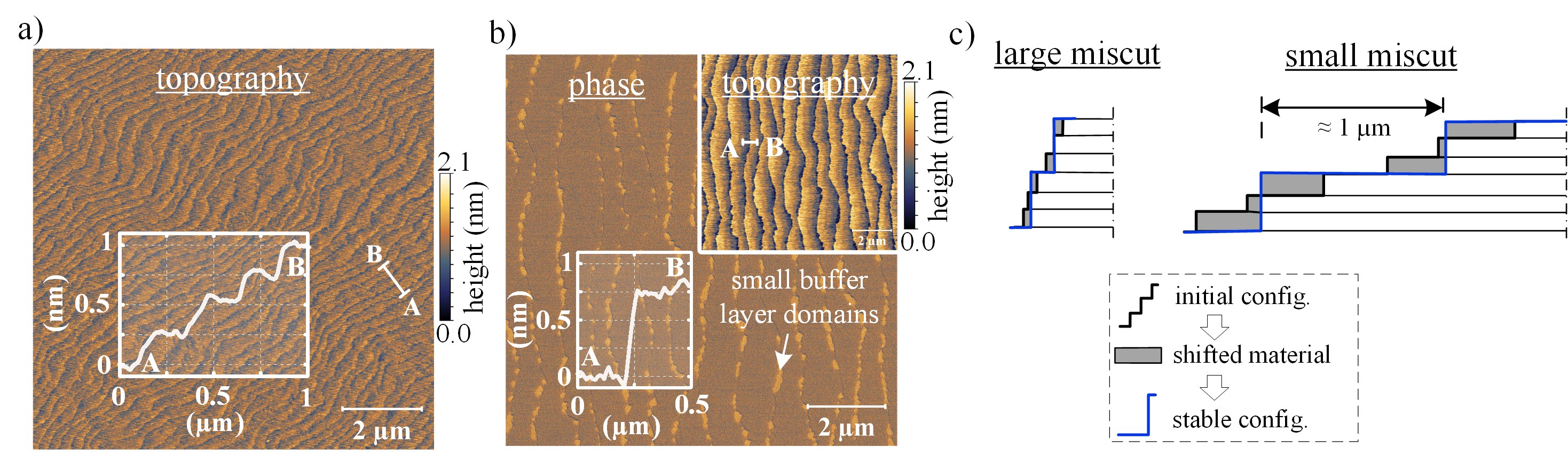
One approach to slow the decomposition of the SiC surface and to prevent giant step bunching is to predefine continuous buffer layer domains using substrates with very low-miscut angles [12, 17, 8]. In this experiment, the annealing procedure at in an argon atmosphere was applied using as-delivered SiC substrate with a small-miscut angle. The AFM image in Figure 5(a) shows the starting surface configuration with single SiC bilayer steps. After annealing regular steps with heights of evolve, see Figure 5(b). The phase image reveals that in addition to SiC (dark contrast), small buffer layer domains (light contrast) form along the energetically preferred lower side of the edges. Steps lower than were not observed since they are not stable and decompose quickly during the initial phase of surface restructuring.
The results imply that during annealing at in argon atmosphere silicon and carbon species may exchange between terraces enabling the formation of a new step configuration and only partly contributing to the buffer layer growth. While this holds also true for the large-miscut substrate the nucleation of the buffer layer is significantly different. This demonstrates that the miscut angle is a critical parameter that strongly influences the dynamics of the restructuring processes. The simplified schematics of surface profiles of large (left) and small (right) miscut surfaces in Figure 5(c) describe the thermally activated conversion of the starting surface configuration (black outline, steps) into the energetically preferred stable configuration (blue outline, steps). The comparison shows that as a result of broader terraces on a small-miscut surface a bigger net mass transfer (gray shaded area) is involved in fulfilling the conversion. The higher amount of released carbon is expected to be the reason for the increased buffer layer coverage and the reduced tendency to form giant steps.
Giant step bunching and buffer layer growth on hydrogen-etched substrate
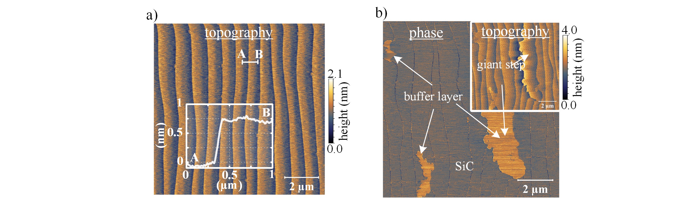
In the following set of experiments, the initial phase of surface restructuring is skipped by using hydrogen-etched samples that were processed at the standard etching temperature of as sketched in Figure 2(c). The corresponding topography in Figure 6(a) shows that in this way the starting surface of the "as-delivered" epi-ready wafer (see Figure 5(a)) is converted into regular bunches of 3 SiC bilayers before the buffer layer growth is initiated. By skipping the restructuring process, its influence on the buffer layer formation can be analyzed. First, a low-temperature post-annealing process step is necessary to desorb remaining hydrogen from the substrate after the hydrogen etching process. Without this process, any subsequent process involving buffer layer or graphene growth is significantly delayed or can be very nonuniform, see supplementary data. The etching and post-annealing procedure results in an extremely clean, (1x1) reconstructed SiC surface with uniform and 0.75nm high steps in agreement with AFM (Figure 6(a)) and low energy electron diffraction (LEED) (data not shown).
Figure 6(b) shows the buffer layer growth on the hydrogen-etched substrate. While most of the terraces remain uncovered and preserve their heights, nucleation of the buffer layer occurs locally at a few randomly distributed sites that are separated by several micrometers. The formation of these sites is accompanied by local step enlargement and further giant step bunching once the step height reaches about 1.5 unit cell heights (2.25 nm). This corresponds to an estimated critical width of about for the small-miscut substrate which is nearly a factor of four wider compared to the critical width identified on large-miscut substrates. From the comparison with the as-delivered small-miscut substrate without applying hydrogen etching (Figure 6) one can conclude that skipping the restructuring process of the SiC surface leads to non-uniform buffer layer nucleation during annealing at in an argon atmosphere. One possible reason for this effect is the absence of nuclei due to the extreme cleanness of the etched surface. Additionally, less carbon is released since the step configuration is already stable and no initial restructuring takes place. Therefore, the first domains must have formed by spontaneous nucleation once a critical level of carbon supersaturation is reached. As it was already found in the case of the large-miscut substrate (Figure 3), the formation of each stable domain seems to suppress the formation of others in their vicinity by locally reducing the level of supersaturation.
Buffer layer nucleation and suppression of giant step formation by surface polymer treatment
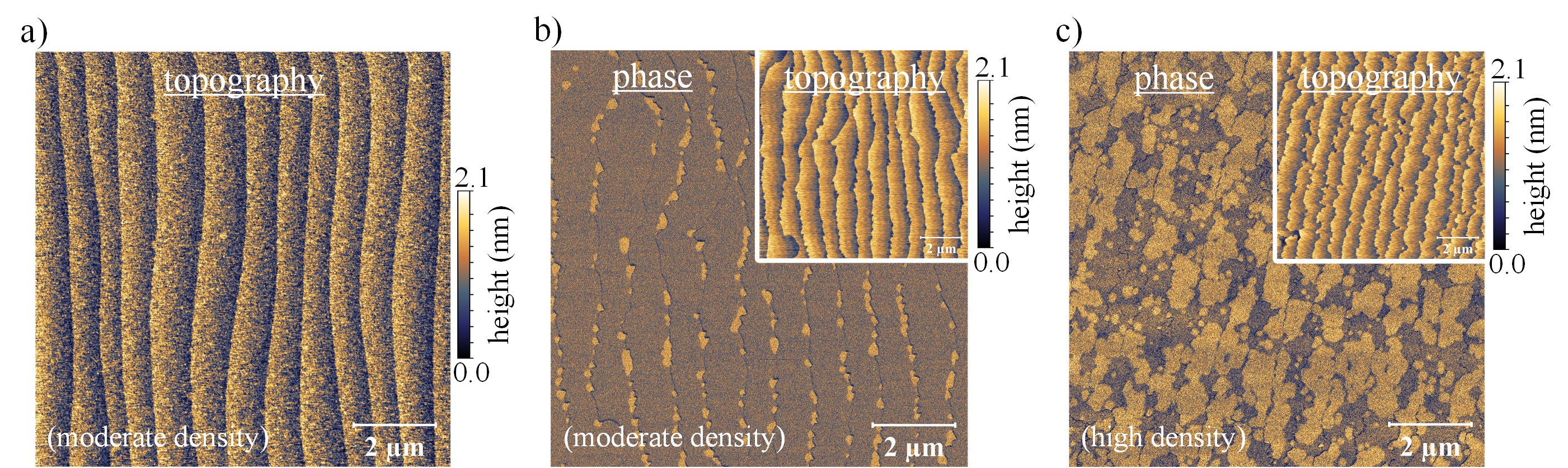
The following set of experiments is a direct comparison to the results shown in Figure 6 using the same annealing procedure as well as hydrogen-etched SiC surfaces. The samples presented in Figure 7 were additionally treated with a polymer adsorbate which supports the buffer layer formation. The principle of this so-called polymer-assisted sublimation growth (PASG) method [18] is to control the amount of available carbon and related nuclei as described in the sample preparation. The starting surface of the first sample shown in Figure 7(a) was modified with a moderate adsorbate density resulting in increased structure heights of (Figure 7(a)).
Indeed, after annealing at in an argon atmosphere, the topography of the two PASG buffer layer samples (Figure 7(b-c)) showed no giant step bunching which is in contrast to the hydrogen-etched substrate without polymer treatment (Figure 6(b)). However, the results are remarkably similar compared to that observed on the as-delivered small-miscut substrate shown in Figure 5(b) even though the starting surfaces were different before annealing and only the etched surface was treated with the polymer. On both surfaces uniformly distributed buffer layer domains formed along the lower side of each step edge and act as preferred nucleation sites. In a second experiment (Figure 7(c)), a hydrogen-etched sample was treated with with a higher adsorbate density as described in the sample preparation. Due to the larger amount of available carbon, the buffer layer coverage significantly increased. These results show that carbon which is released during the restructuring process of the SiC substrate may be substituted by the carbon from the deposited polymer leading to enhanced nucleation and forming a high density of buffer layer domains. The seeded growth prevents the spontaneous formation of large and separated domains and thus the concomitant giant step bunching.
Step-edge and terrace-nucleation models
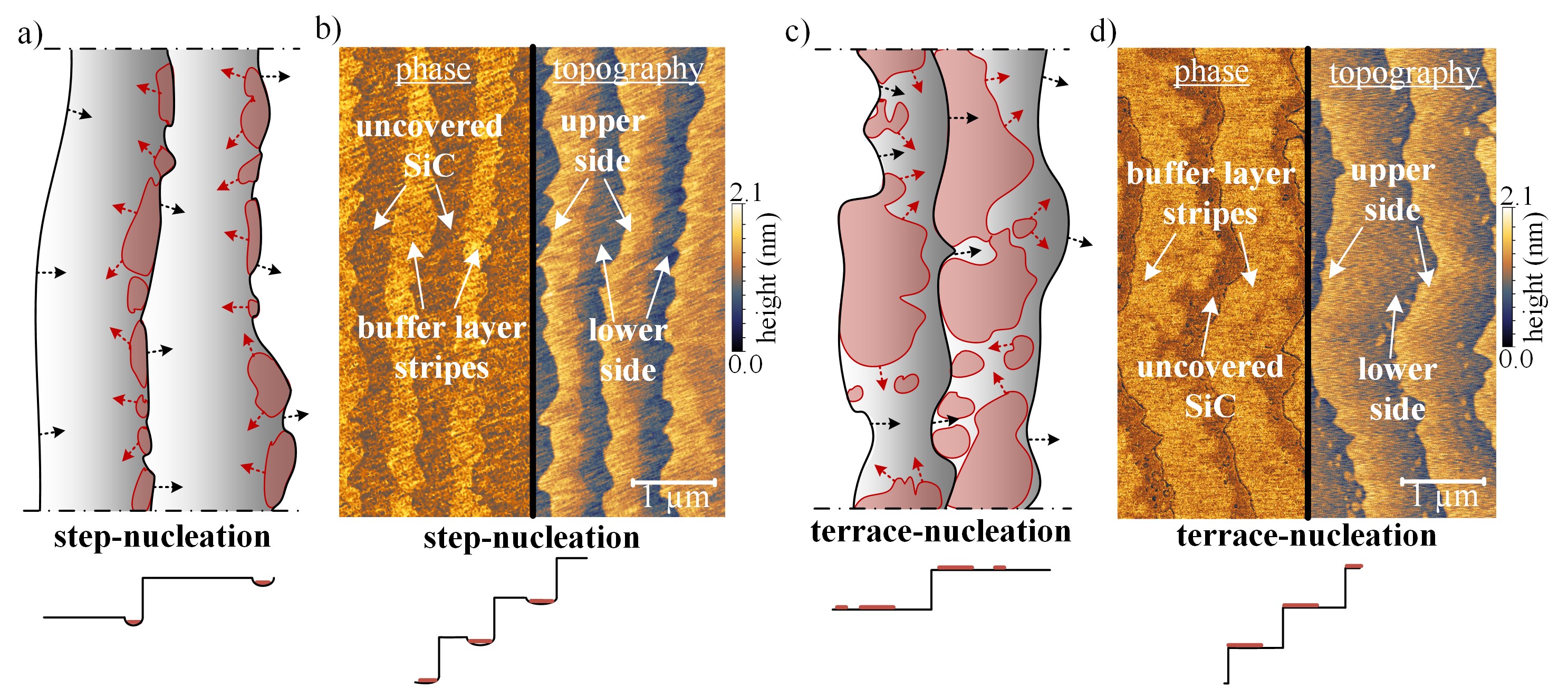
From the different shapes and the location of the buffer layer domains at terrace or edge sites one can distinguish between two different mechanisms of 2D-island growth (Figure 5(b) and Figure 7(b-c)). Depending on the amount of available carbon a transition from one to the other type can be obtained. The first is called “step-nucleation” (Figure 8(a-b)) and describes the case where small domains form along the lower side of step edges. Based on the theory of heteroepitaxy, nucleation at step edges implies near equilibrium growth conditions with a diffusion length larger than the terrace width () such that the species have sufficient time to migrate on the terrace until a stable edge position is found [32, 24]. The comparison of the morphology described in Figure 8(a) and that of the AFM measurements in Figure 8(b) shows increasing the annealing time by leads to the formation of continuous buffer layer stripes (light phase contrast) along the lower side of the edges from where they continue to grow onto the terrace. The measurements indicate that the growing domains are fed from decomposing step edges as well as from crystal layers from underneath since they are typically located slightly lower than the height level of the SiC surface as indicated in the step profiles. The second type of 2D-layer growth shown in Figure 8(c-d) is called “terrace-nucleation” and describes the case where buffer layer domains form on the terraces and not along the step edges. Based on theory, nucleation on the terrace is obtained under supersaturated conditions once the effective diffusion length becomes smaller than the terrace width [32, 24]. On the SiC surface, the reduction of leading to a transition from step-nucleation to terrace-nucleation of buffer layer nuclei is achieved by increasing the amount of the deposited carbon. Figure 8(c) depicts the morphology identified in Figure 7(c) with randomly distributed domains. The sketched surface profiles (below) and the AFM images in Figure 8(d) show that in the case of longer annealing times the distributed islands coalesce and form continuous domains which align along the upper side of the terrace edges.
Graphene formation on hydrogen-etched polymer-treated surfaces
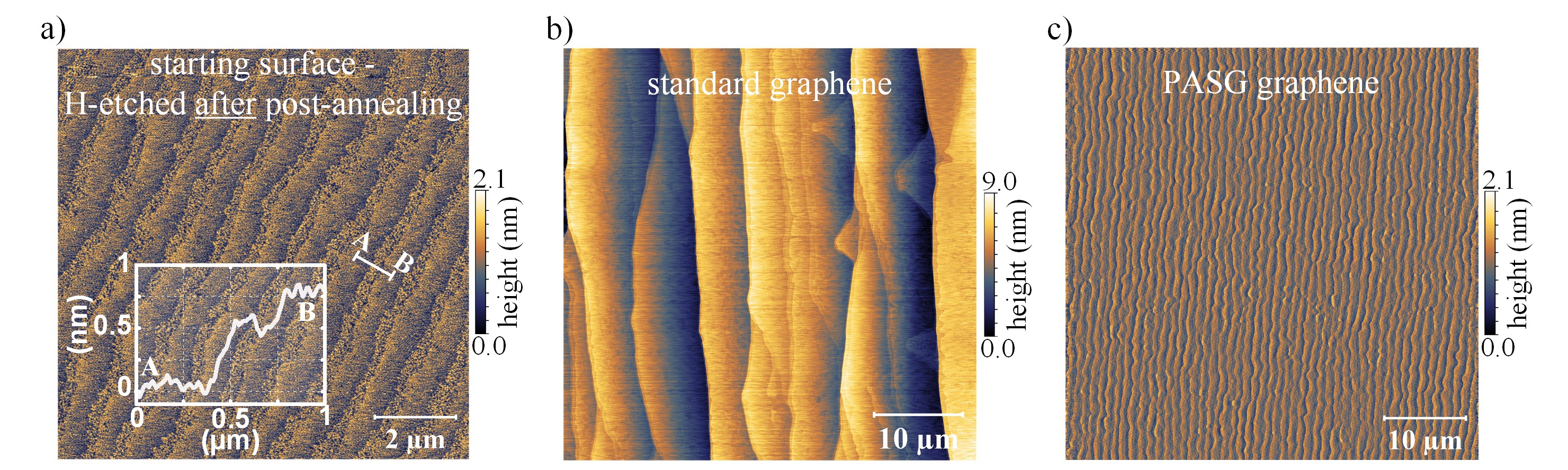
The significance of the predefined buffer layer on the graphene growth process can be well demonstrated using simultaneously processed hydrogen-etched surfaces. Compared to the etched surface in Figure 6(a) the step height of was reduced by applying a lower etching temperature of such that a sequence of two steps with heights of and are obtained as shown in Figure 9(a). This incompletely restructured surface is expected to support the buffer layer growth in agreement with the previous experiments. However, graphene growth without polymer treatment (Figure 9(b)) led to broad terrace structures with heights of up to . Compared to the result after buffer layer growth (Figure 6(b)), giant step bunching is significantly enhanced during graphene growth at . Thus, the slightly reduced step heights and the buffer layer formed during annealing in argon atmosphere alone cannot sufficiently stabilize the surface. This behavior is typical for hydrogen-etched substrates [25, 11]. The previous experiments in Figure 7(b-c) showed that the application of polymer adsorbates successfully circumvent giant step bunching at . The PASG graphene sample shown in Figure 9(c) proves that this also holds true for high temperatures. The slightly reduced initial step heights of the etched surface of and lead to small but noticeable improvements in the final topography of the graphene sample e.g. higher terrace uniformity and reduced step heights compared to a hydrogen-etched starting surface with exclusively (not shown). This is expected to be a consequence of the incomplete restructuring process of the surface before the buffer layer, and graphene growth processes are initiated. The realization of large-area growth of monolayer graphene with step heights on hydrogen-etched substrates demonstrates the versatility of the PASG method and underlines the high importance of the buffer layer formation.
Conclusion
Understanding the morphological changes that occur during the restructuring of the SiC surface lead to significant improvements in the concept of large-area graphene growth. The identified critical point is the conversion of the starting surface into the next stable configuration which is usually accompanied by 2D-island growth of the buffer layer. Three different growth mechanisms were identified namely (i) surface-reconstruction-induced giant step formation as well as buffer layer formation by (ii) step-nucleation or (iii) terrace-nucleation. Their occurrence is closely connected to the properties of the surface and the selected process conditions e.g. the carbon supply. Surface-reconstruction-induced giant step bunching usually occurs when the initial restructuring process of the starting surface involves only a small amount of carbon as it was demonstrated using clean as-delivered large-miscut or hydrogen-etched substrates. Here, the high mobility mass transport between adjacent terraces involving surface diffusion as well as between distant terraces involving desorption and adsorption favors the formation of separated buffer layer domains. The observed mechanisms reveal that the widening of covered terraces is due to the locally created energetically favorable surface configuration of the buffer layer reconstruction. This behavior can be prevented throughout the whole graphene formation process if a high density of small buffer layer domains is grown using suitable substrates and an additional carbon source. Moderate carbon supply favors step-nucleation along the lower side of step edges and usually results in a low coverage. Increasing the amount of available carbon, however, realizes a transition from step-nucleation to terrace-nucleation. Terrace-nucleation under highly supersaturated conditions was identified to be the ideal growth mode since it enables to conserve the lowest possible step heights throughout the whole graphene process and extends the range of suitable substrates. The manipulation of the growth dynamics by seeded buffer layer growth suppresses critical step bunching mechanisms and makes uniform buffer layer growth also possible for hydrogen etched substrates. These results are of particular importance for the large-area growth of monolayer graphene on SiC with ultra-low steps.
Acknowledgements
We gratefully acknowledge funding by the School for Contacts in Nanosystems (NTH nano) and the support by the Braunschweig International Graduate School of Metrology (B-IGSM) and NanoMet.
References
References
- [1] Vlachos D G, Schmidt L D and Aris R 1993 Physical Review B 47 4896–4909
- [2] Schwoebel R L and Shipsey E J 1966 Journal of Applied Physics 37 3682–3686
- [3] Schwoebel R L 1968 Journal of Applied Physics 40 614–618
- [4] Weeks J D and Gilmer G H 2007 Dynamics of Crystal Growth (Preprint 0110319)
- [5] Råback P 1999 Modeling of the Sublimation Growth of Silicon Carbide Crystals Phd thesis Helsinki University of Technology
- [6] Tromp R M and Hannon J B 2009 Physical Review Letters 102 106104
- [7] Ohta T, Bartelt N C, Nie S, Thürmer K and Kellogg G L 2010 Physical Review B 81 121411
- [8] Kruskopf M, Pierz K, Wundrack S, Stosch R, Dziomba T, Kalmbach C C, Müller A, Baringhaus J, Tegenkamp C, Ahlers F J and Schumacher H W 2015 Journal of Physics: Condensed Matter 27 185303
- [9] Starke U and Riedl C 2009 Journal of physics. Condensed matter 21 134016
- [10] Riedl C, Coletti C and Starke U 2010 Journal of Physics D: Applied Physics 43 374009 ISSN 0022-3727
- [11] Oliveira M H, Schumann T, Ramsteiner M, Lopes J M J and Riechert H 2011 Applied Physics Letters 99 111901
- [12] Virojanadara C, Yakimova R, Osiecki J R, Syväjärvi M, Uhrberg R I G, Johansson L I and Zakharov A A 2009 Surface Science 603 L87–L90
- [13] Borovikov V and Zangwill A 2009 Physical Review B 80 121406
- [14] Yazdi G R, Vasiliauskas R, Iakimov T, Zakharov A, Syväjärvi M and Yakimova R 2013 Carbon 57 477–484
- [15] Ming F and Zangwill A 2011 Physical Review B 84 115459 (Preprint 1011.4096)
- [16] Bao J, Yasui O, Norimatsu W, Matsuda K and Kusunoki M 2016 Applied Physics Letters 109 081602
- [17] Virojanadara C, Yakimova R, Zakharov A A and Johansson L I 2010 Journal of Physics D: Applied Physics 43 374010
- [18] Kruskopf M, Momeni Pakdehi D, Pierz K, Wundrack S, Stosch R, Dziomba T, Götz M, Baringhaus J, Aprojanz J, Tegenkamp C, Lidzba J, Seyller T, Hohls F, Ahlers F J and Schumacher H W 2016 2D Materials 3 041002
- [19] Nakagawa H, Tanaka S and Suemune I 2003 Physical Review Letters 91 226107
- [20] Nakajima A, Yokoya H, Furukawa Y and Yonezu H 2005 Journal of Applied Physics 97 104919
- [21] Dhanaraj G, Byrappa K, Prasad V and Michael D 2010 Springer Handbook of Crystal Growth (Berlin, Heidelberg: Springer Berlin Heidelberg) ISBN 978-3-540-74182-4
- [22] Weeks J D, Liu D J and Jeong H C 1997 Dynamics of Crystal Surfaces and Interfaces 20742 199–216
- [23] Jeong H C and Weeks J D 1998 Physical Review B 57 3939–3948
- [24] Lui W K and Santos M B 1999 Thin Films: Heteroepitaxial Systems (Singapore: World Scientific Publishing Company) ISBN 9810233906
- [25] Emtsev K 2009 Electronic and structural characterizations of unreconstructed SiC (0001) surfaces and the growth of graphene overlayers Ph.D. thesis Friedrich-Alexander-Universität Erlangen-Nürnberg
- [26] Yang Y, Cheng G, Mende P, Calizo I G, Feenstra R M, Chuang C, Liu C W, Liu C I, Jones G R, Hight Walker A R and Elmquist R E 2017 Carbon 115 229–236
- [27] de Heer W A, Berger C, Ruan M, Sprinkle M, Li X, Hu Y, Zhang B, Hankinson J and Conrad E 2011 Proceedings of the National Academy of Sciences 108 16900–16905
- [28] Ytrehus T and Østmo S 1996 International Journal of Multiphase Flow 22 133–155
- [29] Gusarov A V and Smurov I 2002 Physics of Fluids 14 4242
- [30] Jeong H C and Weeks J D 1995 Physical Review Letters 75 4456–4459
- [31] Dubrovskii V G 2014 Nucleation Theory and Growth of Nanostructures NanoScience and Technology (Berlin, Heidelberg: Springer Berlin Heidelberg) ISBN 978-3-642-39659-5
- [32] Hasselbrink E and Lundqvist B I 2008 Handbook of Surface Science Vol. 3 (Liverpool, UK: Elsevier) ISBN 9780444520562
See pages - of StudyOnTheMorphologyAndGrowth_SupplementaryData