nm aboard, about above absent according to across after against ahead of along alongside amid amidst among around as as far as as well as at atop before behind below beneath beside between by by means of despite down on to (onto) opposite out of outside outside of owing to over past plus prior to regarding round save since than through throughout till times to toward under underneath until up upon with with regards to within without due to during except far from following for from in in addition to in case of in front of in place of in spite of inside inside of instead of in to into like mid minus near near to next next to notwithstanding of off on on account of on behalf of on top of both and not only but also either or neither nor whether or as as such that scarcely when as many as no sooner than rather than and but rr nor for yet so after although as as if as long as as much as as soon as as though because before even even if even though if if only if when if then inasmuch in order that just as lest now now since now that now when once provided provided that rather than since so that supposing than that though til unless until when whenever where whereas where if wherever whether which while who whoever why IBM Research - Zurich]IBM Research - Zurich, Rueschlikon 8803, Switzerland IBM Research - Almaden]IBM Research - Almaden, San Jose, CA 95120 USA. IBM Research - Zurich]IBM Research - Zurich, Rueschlikon 8803, Switzerland
Accurate Location and Manipulation of Nano-Scaled Objects Buried under Spin-Coated Films
Abstract
Detection and precise localization of nano-scale structures buried beneath spin coated films are highly valuable additions to nano-fabrication technology.
In principle, the topography of the final film contains information about the location of the buried features. However, it is generally believed that the relation is masked by flow effects, which lead to an upstream shift of the dry film’s topography and render precise localization impossible.
Here we demonstrate, theoretically and experimentally, that the flow-shift paradigm does not apply at the sub-micron scale. Specifically, we show that the resist topography is accurately obtained from a convolution operation with a symmetric Gaussian Kernel whose parameters solely depend on the resist characteristics. We exploit this finding for a 3 precise overlay fabrication of metal contacts to an InAs nanowire with a diameter of 27 using thermal scanning probe lithography.
Keywords: spin coating; subsurface imaging; atomic force microscopy; thermal scanning probe lithography; maskless lithography
The identification of buried features is of interest in a wide range of fields, including biology 1, polymer physics 2 and semiconductor fabrication 3. A number of techniques exist for detecting micron-scaled features, for example sonography and confocal microscopy. However, nondestructive options at the nanometer scale are more limited. Transmission Electron Microscopy has been shown to be capable of imaging carbon nanotubes in cells 4. Methods based on the ubiquitous atomic force microscope offer the potential for nondestructive imaging at nanometer resolution without the need for careful sample preparation. An early AFM-based technique capable of detecting buried features employed a high-frequency acoustic wave 5 and a tip detection scheme. Recently, it has been shown that the amplitude modulation operating mode of AFM can be used to detect buried features 2, 6 beneath soft films.
The detection of objects buried beneath spin-coated films is of particular interest given the widespread use of spin coating to prepare resist films with precisely controlled thickness. As a consequence, spin coating resides at the heart of micro- and nanofabrication and is part of many of the standard processes, in particular those involving lithography, such as pattern transfer, metal lift-off and local ion implantation. It has been shown that substrate topography leads to a disturbance of the surface of the spin-coated film 7, 8, 9, 10, 11, 12, 13, 14, 15, 16. The effect impairs the flatness or planarity of the final film and has long been of concern to the semiconductor industry. Previous work has shown that for large () features, this relationship strongly depends on the local direction and rate of fluid flow during spin coating 17, 18 (see figure 1).
However, this residual topography in principal offers a straightforward means of locating existing structures buried beneath the spin-cast film using surface-sensitive techniques, such as scanning probe microscopy (SPM). Provided nanometer precision in the detection of buried feature position is possible, this approach can assist in the development of a quantitative understanding of other sub-surface techniques 19, 20 on model substrates. Moreover, precise location of features buried beneath spin-coated films would provide a direct means for addressing the critical challenge of overlay accuracy for device fabrication. Scanning probe lithography (SPL) tools 21 can readily measure nanometer-scale topography as well as transfer sub-20 features into silicon, 22 and thus provide a unique method for nanometer-precise device fabrication.
In this paper, we demonstrate that for sub-micron sized features the relationship between surface and sub-surface topography becomes independent of the flow direction. We show analytically that for the limiting case of small sub-surface topography the surface topography may be obtained by convolving this sub-surface topography with a kernel that is well approximated by a Gaussian. The model is then validated for the widely used resist Polymethylmethacrylate (pmma) for in-plane length-scales spanning 10-1000 nm. We show that the residual topography may be predicted after calibration of the resist-solvent system and further that the topography may be enhanced by an additional solvent annealing and quenching step. Finally, we demonstrate the utility of this approach for addressing nano-scale devices by scanning probe lithography.
1 Results and Discussion
1.1 Phases of Spin Coating
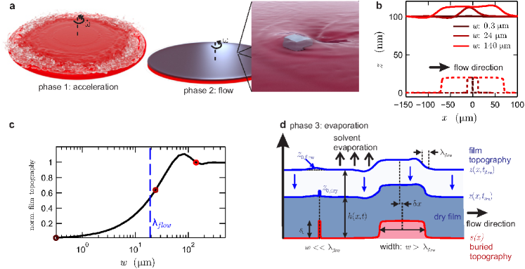
The spin-coating process may be divided into three distinct phases 23, see Figure 1. The first phase involves the rapid angular acceleration of the dispensed spin-coating solution as the substrate begins to rotate 24. Under the influence of the inertial forces, the fluid spreads on the surface. When the liquid layer has become sufficiently thin, 25 the so-called “flow phase” begins, in which the fluid moves radially at a low Reynolds number under the influence of the inertial force 23. The strong dependence of the flow rate on the film thickness causes the latter to progress towards a conformal coating of the wafer 26. If topography is present on the surface a competition arises between the surface tension, which seeks to level the film, and the inertial term, which seeks to maintain a uniform film thickness 27, see Figure 1b. The final “evaporation phase”, which was identified by Meyerhofer 28, follows the flow phase. In the evaporation phase, flow is negligible and film thinning is dominated by solvent evaporation, see Figure 1d.
The significant difference between the in-plane and out-of-plane length scales for the film encountered in spin coating allows the reduction of the Navier Stokes and continuity equation to the so-called Lubrication approximation 29 for the film thickness ():
| (1) |
where is the surface tension, is the fluid viscosity, (see figure 1a) is the buried topography and is the volume of evaporated solvent per unit area 15. For the case of spin coating, a body force term is added to account for the rotation of the film’s co-ordinate system. The lubrication approximation has been found to be accurate to better than 10% peak error even for flows over sharp steps whose height is on the order of the film thickness 30, 31, 32. Previous workers have solved the coupled system of equations numerically for flat surfaces 28, 23, 33, 25, 34 and surfaces exhibiting radial symmetry but containing (10)-sized features 12, 13.
Useful insight into the relevant in-plane length scale for the flow phase () may be obtained from the approximate analytical solutions of refs. 11 and 14 for the flow phase. The authors show that the flow over a radially symmetric step located at may be constructed from a set of three linearly independent terms which decay as . is a constant of order unity and is given by
| (2) |
where is the fluid density, is the sample’s angular velocity, and is the radial position of the buried feature. Substituting reasonable values of Nm-1, nm, rpm, kgm-3 and mm yields m. The results of a numerical calculation of the flow over a radially symmetric feature with a rectangular cross section are shown in figures 1b and 1c (see methods section for details). Features whose width exceeds result in a change in height of the fluid’s upper surface that is equal to the height of the buried feature. Conversely, if the free surface remains almost flat above the buried feature.
1.2 Final Topography: Small Structures ()
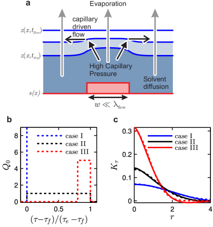
For features whose width is less than m (see figure 1c), the topography present in the film surface as the evaporation phase begins is a few percent of the sub-surface topography. As such, its contribution to the surface topography of the dry film is dominated by the additional topography emerging during the evaporation phase. Previous workers 8, 11 have made the assumption that the topography formed during the evaporation phase may be calculated by assuming a uniform shrinkage of the film present as the evaporation phase starts. Here we refine this assumption by observing that it predicts the transfer of sharp step-like features from the sub-surface topography to the film topography. The development of such a sharply curved surface would be opposed by the surface tension, which would cause the film to flow, see Figure 2. The competition between evaporation-driven topography formation and capillary flattening proceeds until the polymer matrix becomes glassy and solvent evaporation ceases.
1.3 Analytical Solution
We make several approximations to allow for an analytical treatment of the evaporation phase. Firstly, the body-force term is assumed to be negligible during this phase. Secondly, we retain the assumption used for large structures that the loss of solvent per unit area is proportional to the film thickness at the end of the flow phase. Thus the evaporation term in equation (1) becomes
| (3) |
where is the evaporation rate per unit initial film thickness during the evaporation phase, is the time at which the flow phase ends and is the film thickness far from any topographic features at .
Equation (1) can now be solved for the approximation of equation (3) and for an asymptotic expansion. The rapidly varying viscosity is treated as a known function of time at this stage. This yields the pair of equations for the first two terms in the expansion where and :
| (4) | |||
| (5) |
Given , equation (4) may be integrated to obtain the uniform thinning of the film due to evaporation. Equation (5) can also be readily integrated by first defining a re-scaled time parameter to accommodate the changing mobility of the film with and :aaaThe variation of the surface tension with solvent concentration can also be handled by conceptually making . This does not account for the in-plane variation of the concentration required to achieve the faster evaporation rate.
| (6) |
Note that the viscosity eventually diverges so that goes to some finite value as . Substituting this change of variable into equation (5) yields
| (7) |
The variable describes the evaporation rate scaled by the film’s ability to flow in the face of the emerging topography. We are interested in the profile of the dry film , which is given by
| (8) | ||||
| (9) | ||||
| (10) |
where denotes convolution and is the Green’s function for equation (7):
| (11) |
where is a Bessel’s function of the first kind.
The usefulness of preceeding analysis is derived from the insensitivity of the shape of to the form of . Figure 2b shows three quite different profiles for . Figure 2c shows the corresponding values for for each case. Each of these curves is well approximated by a Gaussian, with the exception of the evanescent small amplitude oscillations at large . Thus may be described in terms of just two parameters, the Gaussian’s width and its amplitude :
| (12) |
Case III of figure 2b is likely closest to the physical , which corresponds to a formation of topography towards the end of the evaporation phase when the film is relatively less able to level itself. Initially the rate of solvent loss is controlled by evaporation from the film interface 23, 12. As such, in equation (7) will fall linearly with the solvent concentration 35. As falls, will increase as a power law 36, 28, 33, 13 in (1-) with an exponent of . It may also be readily shown that during the evaporation phase . At some value of , or equivalently , will, if plotted on a linear scale, rise rapidly. This corresponds to the left-hand edge of the pulse shown in figure 2b. The value of will be limited by the falling . Its rate of reduction is accelerated by the declining diffusivity of the solvent in the solution. Initially this diffusivity is rather insensitive to the falling concentration; 23 however below a critical concentration, the diffusivity drops rapidly. For solutions of Polystyrene and Toluene, this critical concentration was identified as 20% 12. At this concentration it may be anticipated that the polymer matrix has begun to form and that has reached , signaling the end of the evaporation phase.
In this section, we have derived a simple description of the relationship between the buried and the dry film topography after spin coating. In contrast to solutions obtained on large structures, where the flow phase dominates topography formation, the film topography is predicted to be vertically aligned with that of the substrate. In a complete calculation, the dependence of the solvent diffusivity and the solution viscosity must first be measured as a function of solvent concentration. In contrast, here the model is parameterised by a measurement of and for the film thickness of interest.
1.4 Model Validation
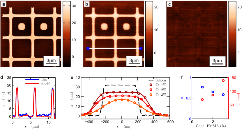
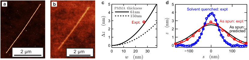
Figure 3a and 3b show AFM images of a patterned silicon surface before () and after () the addition of an 86-thick layer of pmma spin coating. The two images have been aligned by scratching the sample just below the portion of the AFM image shown in figures 3a and 3b (see figure S4).
From figures 3c and 3d, it can be seen that there is good agreement between the model’s prediction and experiment for the obtained fit parameters of [see equation (12)] = 0.69 and . There is no observable translational offset between the surface and buried features. There is also no significant error irrespective of the wire orientation or near the ends of the wires, suggesting that the model is not solely able to predict the topography over wire-like features. Similar experiments have been performed with the commercial resist HM8006 manufactured by JSR Micro. These experiments yielded results consistent with those obtained for PMMA (see figure S3).
Similar results were also obtained for solutions with concentrations varying from 1% to 3% spin coated over the wire structures shown in figure 3a. We measured the topography and used a least squares fit to identify the values of and for each concentration, see figure 3e and f. , which is representative of the length scale for the flow during the evaporation phase, increases with increasing film thickness. This makes conceptual sense, given the strong () dependence of the flow rate on the film thickness which increases with concentration. We likely do not observe a cubic dependence because the strong sensitivity of the viscosity on the concentration partially cancels the term. The dependence of on the concentration also makes intuitive sense. More concentrated solutions, which lead to thicker films, result in greater planarisation of the surface.
Using interpolation of the data presented in figure 3f, the Kernel function for a film spun from a pmma solution of arbitrary initial concentration may be calculated. Knowledge of this Kernel in turn allows prediction of the dry-film topography for an arbitrary sub-surface topography, provided . To test the predictive power of our model, we dispersed InAs nanowires onto a silicon substrate. One such wire having a diameter of 27 and a length of roughly 6 is shown in figure 4a. We spin coated a 60 pmma film onto the surface, which corresponded to a pmma concentration of 1.5%. The surface topography of the wire after the spin-coating process is shown in figure 4b. The measured cross section of the wire is indicated by the red circles in figure 4d. Figure 4c shows the predicted topography amplitude over the nanowire for two film thicknesses and a range of nanowire diameters. Linear interpolation was used in the calculation, and the nanowire cross section was approximated as a square of side . The experimental result, corresponding to , is also shown in figure 4c. The predicted cross section is shown as the black line in figure 4d.
There is good agreement between the predicted and measured cross sections. The error in the peak height is just 10%. This is particularly encouraging because the Kernel was parameterised using measurements on a structure that was more than an order of magnitude larger than the nanowire. The red line in figure 4e shows the least squares fit of a Gaussian to this experimental data. The high fit quality may be anticipated as the nanowire is much narrower than . As such, the topographic feature behaves like the Dirac distribution, so that the measured cross-section is approximately , which is itself a Gaussian function. The result provides direct evidence that the form derived for is appropriate. The value of interpolated from the calibration data was 80, which is in good agreement with the fitted value of 68. A similar accuracy could be achieved when treating the inverse problem of re-constructing the buried topography from the measured film topographybbbOf course, the usual limitations would apply to the recovery of spatial frequencies above ..
We note that so-called tip convolution effects 37, which are a well known source of artifacts in AFM images, will not affect the results discussed here. Our homemade tSPL probes have a typical radius of 5 (see figure S10a) which is significantly less than the measured value for . Thus, as shown in the supporting information, the effect of tip convolution on our measured film topographies (see figures S9 and S10) is negligible.
Our spin-coating model predicts that the width of should be reduced if the evaporation process is sped up. To investigate this experimentally, we swelled the film shown in figure 4b in saturated dichloromethane (DCM) vapour for several minutes. The cross section of the nanowire was then re-measured using AFM. The results of this measurement are shown by the blue circles in figure 4d. Assuming that in the swollen state the capillary forces are able to flatten the surface of the film, we expect the same physics to control the topography formation as in the case of spin coating. Consequently, the cross section of the film topography above the wire (blue line, figure 4d) is once again well fitted by a Gaussian. The fitted value of is smaller by a factor of 0.47, which is consistent with the higher vapor pressure of DCM (360 kPa) as compared to anisol (46 kPa). This experimental result is of significant technological value. Use of this volatile solvent has enhanced both the amplitude and the sharpness of the pattern, allowing it to be more accurately detected in the AFM. Exposure after spinning avoids the difficulties associated with spinning from a highly volatile solvent that can lead to films exhibiting high surface roughness 38, 39.
The theory outlined so far provides a simple means of predicting how the topography over a buried feature will change as the thickness of the spin coated layer increases. As the layer becomes thicker, the signal will become weaker and will eventually become lost in the detection noise. The detection noise originates from the electronic noise of the instrument and the surface roughness of the spin-coated polymer 42. The problem of predicting the error in feature position due to noise has been considered previously, and details are given in ref. 41.
1.5 Application
We close by applying our markerless overlay approach to the fabrication of electrodes used to contact a nanowire. The transfer of a pattern from the resist layer to the substrate provides a direct experimental means of confirming that the resist topography is not shifted with respect to buried features.
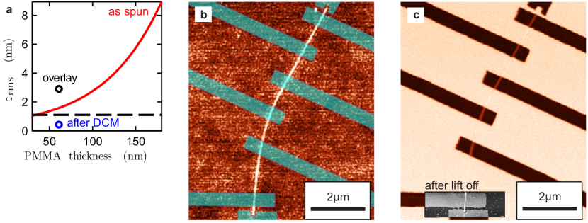
Figure 5a shows the expected error when detecting the transverse position of the nanowire as a function of the film thickness 41. A pmma film thickness of 60 nm was selected to balance the requirements of overlay accuracy and succesful lift-off of the evaporated metal film. After the spin-coating process, the nanowire was exposed to the DCM atmosphere, which resulted in an improvement in the amplitude and sharpness of the pattern. These improvements reduced the expected position detection error when locating the position of the wire to less than 1 (see figure 5a).
Figure 5b shows an AFM image of the nanowire taken by the tSPL tool prior to patterning. The intended position of the contact pads with respect to the wire are shown by the transparent blue overlay. Figure 5c shows the device topography following tSPL patterning and etching. The nanowire is visible at the bottom of each etched trench. Figure 5c has been aligned with the contact pad design shown in blue in figure 5b using the cross-correlation based approach discussed in ref. 41. It can be seen qualitatively that the portions of the nanowire which are visible at the bottom of the etched trenches are aligned with the residual surface topography. Cross-correlation was used to locate the position of the exposed parts of the nanowire shown in figure 5c with respect to the topography shown in figure 5b (see figures S6-S8). The overlay error perpendicular to the wire’s long axis was measured as 2.9, which compares favourably with the wire’s diameter of 27. This value is somewhat larger than the expected correlation error. This is likely due to three factors. The first is the error in the tSPL instrument which has been measured as 1.1 41. The second is that the sputtering of the SiOx layer damaged the pmma surface, leading to a higher surface roughnesscccFor subsequent devices, the SiOx was deposited using evaporation, which did not lead to an increase in surface roughness.. Finally, the reactive ion etch has introduced some edge roughness. While this overlay error may not achieve the limit expected for the tool, it does provide further evidence that the topography of the dry film is precisely aligned with the sub-surface topograpy.
2 Conclusion
In this paper, we have shown theoretically and experimentally that spin coating across structures of feature widths results in a residual topography that is vertically aligned to the buried features. This alignment occurs because at this length scale, the flow phase of the spin-coating process does contribute significantly to the topography of the dry film. Even for nanoscaled buried features the perturbation of the dry film topography may be readily measured using an AFM. The lateral position of buried features can therefore be determined using cross correlation with sub-nanometer accuracy. Good prediction of the final topography is possible by simply convolving the buried topography with a Gaussian Kernel. The Kernel may be parameterised through measurements on arbitrary features for which . Using insight gained from the model, we have proposed a simple post-spin processing step whereby the dry film is exposed to a highly volatile solvent. In our case, this process reduced the detection error for the buried feature by a factor of three to a value of less than 1. Finally, we demonstrated the technological relevance of this work by performing markerless lithographic overlay onto a nanowire. We achieve an overlay error below 3 or roughly one tenth of the nanowire diameter. This opens up a number of exciting possibilities in the experimental investigation of nanostructures.
3 Methods
3.1 Calculation of fluid flows over wires
The profiles of figures 1b and 1c were obtained by solving equation (1) for . It is shown in ref. 11 that for radially symmetric topography located far from the axis of rotation, equation (1) may be simplified to
| (13) |
This ordinary differential equation was solved numerically on the interval using the scripting language Matlab. The equation for was recast as a set of three first-order differential equations subject to the boundary conditions , , and then supplied to the in-built function bvp5c for solution. The sharp step occurring at the edge of the wire was approximated by 11 , with . The third-order derivative was obtained from this function analytically. For small values of , the accurate numerical solution of equation (13) becomes increasingly time consuming. Thus, following ref. 11, equation (13) was reformulated on the variable and then expanded to first order to yield . This equation was then solved analytically for the case of an ideal step (). The result of the approximate analytical solution was compared with the numerical solution for , and found to agree to within 5% over this range of . The data in figures 1b and 1c relating to values of was computed from the analytical solution.
3.2 Spin Coating
Substrates with topography were prepared from silicon wafers using optical lithography. Following exposure and development of the resist, the pattern was transferred into silicon by etching with hydroflouric acid. Additional substrates were prepared by dispersing InAs nanowires onto a flat silicon surface. Films were spin coated using a Laurell Technologies WS-650 spin coater. The 950pmma A resist solution used in the spin-coating process was prepared by Micro Chem from pmma and anisole. It was spun at 2000 for 80 seconds. Concentrations below 2% were obtained by further dilution of the as-purchased solution in Anisole. AFM measurements were performed using a Digital Instruments AFM operated in tapping mode.
3.3 tSPL patterning
The thermal Scanning Probe Lithography (tSPL) was performed on our home-made system, which has been described in detail elsewhere 43, 44. Our homemade tSPL tool can locally remove the resist, polyphthaladehyde, by means of a tip that has a typical diameter of 10 which is heated several hundred degrees centrigrade. The structured deposition of the nickel layer was achieved using a standard pmma lift-off process. The details of the transfer of the pattern written in the PPA layer into the pmma layer are summarised in the supplemental information (see figure S1) and provided in detail in ref. 22. The details of the pattern-overlay process are given in ref. 41.
The authors gratefully acknowledge the technical assistance of U. Drechsler and S. Reidt. The authors would also like to thank P. Mensch and S. Karg for providing both the nanowires and valuable advice. Finally, the authors are indebted to C. Bollinger for her careful proof reading of the manuscript. The research leading to these results received funding from the European Union’s Seventh Framework Program FP7/2007-2013 under Grant Agreement No. 318804 (Single Nanometer Manufacturing for beyond CMOS devices - acronym SNM) and through the European Research Council StG no. 307079.
Details of the pattern transfer method, the analysis of the organic hardmask HM8006, and the pattern registration (Figures S1-S10).
References
- Tetard et al. 2008 Tetard, L.; Passian, A.; Venmar, K. T.; Lynch, R. M.; Voy, B. H.; Shekhawat, G.; Dravid, V. P.; Thundat, T. \titlecapImaging nanoparticles in cells by nanomechanical holography. Nat. Nanotechnol. 2008, 3, 501–505
- Spitzner et al. 2011 Spitzner, E.-C.; Riesch, C.; Magerle, R. \titlecapSubsurface Imaging of Soft Polymeric Materials with Nanoscale Resolution. ACS Nano 2011, 5, 315–320
- Shekhawat and Dravid 2005 Shekhawat, G. S.; Dravid, V. P. \titlecapNanoscale Imaging of Buried Structures via Scanning Near-Field Ultrasound Holography. Science 2005, 310, 89–92
- Porter et al. 2007 Porter, A. E.; Gass, M.; Muller, K.; Skepper, J. N.; Midgley, P. A.; Welland, M. \titlecapDirect imaging of single-walled carbon nanotubes in cells. Nat. Nanotechnol. 2007, 2, 713–717
- Cuberes et al. 2000 Cuberes, M. T.; Assender, H. E.; Briggs, G. A. D.; Kolosov, O. V. \titlecapHeterodyne force microscopy of PMMA/rubber nanocomposites: nanomapping of viscoelastic response at ultrasonic frequencies. J. Phys. D: Appl. Phys. 2000, 33, 2347
- Ebeling et al. 2013 Ebeling, D.; Eslami, B.; Solares, S. D. J. \titlecapVisualizing the Subsurface of Soft Matter: Simultaneous Topographical Imaging, Depth Modulation, and Compositional Mapping with Triple Frequency Atomic Force Microscopy. ACS Nano 2013, 7, 10387–10396
- White 1985 White, L. K. \titlecapApproximating Spun-On, Thin Film Planarization Properties on Complex Topography. J. Electrochem. Soc. 1985, 132, 168–172
- Peurrung and Graves 1991 Peurrung, L. M.; Graves, D. B. \titlecapFilm Thickness Profiles over Topography in Spin Coating. J. Electrochem. Soc. 1991, 138, 2115–2124
- Stillwagon et al. 1987 Stillwagon, L. E.; Larson, R. G.; Taylor, G. N. \titlecapPlanarization of Substrate Topography by Spin Coating. J. Electrochem. Soc. 1987, 134, 2030–2037
- Stillwagon and Larson 1988 Stillwagon, L. E.; Larson, R. G. \titlecapFundamentals of topographic substrate leveling. J. Appl. Phys. 1988, 63, 5251–5258
- Stillwagon and Larson 1990 Stillwagon, L. E.; Larson, R. G. \titlecapLeveling of thin films over uneven substrates during spin coating. Phys. Fluids A 1990, 2, 1937–1944
- Gu et al. 1995 Gu, J.; Bullwinkel, M. D.; Campbell, G. A. \titlecapSpin Coating on Substrate with Topography. J. Electrochem. Soc. 1995, 142, 907–913
- Kucherenko and Leaver 2000 Kucherenko, S. S.; Leaver, K. D. \titlecapModelling effects of surface tension on surface topology in spin coatings for integrated optics and micromechanics. J. Micromech. Microeng. 2000, 10, 299
- Wu and Chou 1999 Wu, P.-Y.; Chou, F.-C. \titlecapComplete Analytical Solutions of Film Planarization during Spin Coating. J. Electrochem. Soc. 1999, 146, 3819–3826
- Wang and Yen 1995 Wang, C.-T.; Yen, S.-C. \titlecapTheoretical analysis of film uniformity in spinning processes. Chem. Eng. Sci. 1995, 50, 989 – 999
- Sukanek 1989 Sukanek, P. C. \titlecapA Model for Spin Coating with Topography. J. Electrochem. Soc. 1989, 136, 3019–3026
- Peurrung and Graves 1993 Peurrung, L.; Graves, D. \titlecapSpin coating over topography. IEEE Trans. Semiconduct. Manufact. 1993, 6, 72–76
- Hayes et al. 2000 Hayes, M.; O’Brien, S. B. G.; Lammers, J. H. \titlecapGreen’s function for steady flow over a small two-dimensional topography. Phys. Fluids 2000, 12, 2845–2858
- Verbiest et al. 2012 Verbiest, G. J.; Simon, J. N.; Oosterkamp, T. H.; Rost, M. J. \titlecapSubsurface atomic force microscopy: towards a quantitative understanding. Nanotechnology 2012, 23, 145704
- Bosse et al. 2014 Bosse, J. L.; Tovee, P. D.; Huey, B. D.; Kolosov, O. V. \titlecapPhysical mechanisms of megahertz vibrations and nonlinear detection in ultrasonic force and related microscopies. J. Appl. Phys. 2014, 115, 144304
- Garcia et al. 2014 Garcia, R.; Knoll, A. W.; Riedo, E. \titlecapAdvanced scanning probe lithography. Nat. Nanotechnol. 2014, 9, 577–587
- Wolf et al. 2015 Wolf, H.; Rawlings, C.; Mensch, P.; Hedrick, J. L.; Coady, D. J.; Duerig, U.; Knoll, A. \titlecapSub 20 nm Silicon Patterning and Metal Lift-Off Using Thermal Scanning Probe Lithography. J. Vac. Sci. Technol., B 2015, 33, 02B102
- Lawrence 1988 Lawrence, C. J. \titlecapThe mechanics of spin coating of polymer films. Phys. Fluids 1988, 31, 2786–2795
- Rehg and Higgins 1988 Rehg, T. J.; Higgins, B. G. \titlecapThe effects of inertia and interfacial shear on film flow on a rotating disk. Phys. Fluids 1988, 31, 1360–1371
- Matar et al. 2005 Matar, O. K.; Lawrence, C. J.; Sisoev, G. M. \titlecapThe flow of thin liquid films over spinning disks: Hydrodynamics and mass transfer. Phys. Fluids 2005, 17, 052102
- Emslie et al. 1958 Emslie, A. G.; Bonner, F. T.; Peck, L. G. \titlecapFlow of a Viscous Liquid on a Rotating Disk. J. Appl. Phys. 1958, 29, 858–862
- Hwang and Ma 1989 Hwang, J. H.; Ma, F. \titlecapOn the flow of a thin liquid film over a rough rotating disk. J. Appl. Phys. 1989, 66, 388–394
- Meyerhofer 1978 Meyerhofer, D. \titlecapCharacteristics of resist films produced by spinning. J. Appl. Phys. 1978, 49, 3993–3997
- Howison 2005 Howison, S. Practical Applied Mathematics: Modelling, Analysis, Approximation; Cambridge University Press, 2005
- Mazouchi and Homsy 2001 Mazouchi, A.; Homsy, G. M. \titlecapFree surface Stokes flow over topography. Phys. Fluids 2001, 13, 2751–2761
- Gaskell et al. 2004 Gaskell, P. H.; Jimack, P. K.; Sellier, M.; Thompson, H. M.; Wilson, M. C. T. \titlecapGravity-driven flow of continuous thin liquid films on non-porous substrates with topography. J. Fluid Mech. 2004, 509, 253–280
- Veremieiev et al. 2010 Veremieiev, S.; Thompson, H.; Lee, Y.; Gaskell, P. \titlecapInertial thin film flow on planar surfaces featuring topography. Comput. Fluids 2010, 39, 431 – 450
- Bornside et al. 1989 Bornside, D. E.; Macosko, C. W.; Scriven, L. E. \titlecapSpin coating: One-dimensional model. J. Appl. Phys. 1989, 66, 5185–5193
- Münch et al. 2011 Münch, A.; Please, C. P.; Wagner, B. \titlecapSpin coating of an evaporating polymer solution. Phys. Fluids 2011, 23, 102101
- Sparrow and Gregg 1960 Sparrow, E. M.; Gregg, J. L. \titlecapMass Transfer, Flow, and Heat Transfer About a Rotating Disk. J. Heat Transfer 1960, 82, 294–302
- Flack et al. 1984 Flack, W. W.; Soong, D. S.; Bell, A. T.; Hess, D. W. \titlecapA mathematical model for spin coating of polymer resists. J. Appl. Phys. 1984, 56, 1199–1206
- Markiewicz and Goh 1994 Markiewicz, P.; Goh, M. C. \titlecapAtomic force microscopy probe tip visualization and improvement of images using a simple deconvolution procedure. Langmuir 1994, 10, 5–7
- Lai 1979 Lai, J. H. \titlecapAn investigation of spin coating of electron resists. Polym. Eng. Sci. 1979, 19, 1117–1121
- Spangler et al. 1990 Spangler, L. L.; Torkelson, J. M.; Royal, J. S. \titlecapInfluence of solvent and molecular weight on thickness and surface topography of spin-coated polymer films. Polym. Eng. Sci. 1990, 30, 644–653
- Cheong et al. 2013 Cheong, L. L.; Paul, P.; Holzner, F.; Despont, M.; Coady, D. J.; Hedrick, J. L.; Allen, R.; Knoll, A. W.; Duerig, U. \titlecapThermal Probe Maskless Lithography for 27.5 nm Half-Pitch Si Technology. Nano Lett. 2013, 13, 4485–4491
- Rawlings et al. 2014 Rawlings, C.; Duerig, U.; Hedrick, J.; Coady, D.; Knoll, A. \titlecapNanometer Accurate Markerless Pattern Overlay Using Thermal Scanning Probe Lithography. IEEE Trans. Nanotechnol. 2014, 13, 1204–1212
- Knoll 2013 Knoll, A. W. \titlecapNanoscale Contact-Radius Determination by Spectral Analysis of Polymer Roughness Images. Langmuir 2013, 29, 13958–13966
- Pires et al. 2010 Pires, D.; Hedrick, J. L.; De Silva, A.; Frommer, J.; Gotsmann, B.; Wolf, H.; Despont, M.; Duerig, U.; Knoll, A. W. \titlecapNanoscale Three-Dimensional Patterning of Molecular Resists by Scanning Probes. Science 2010, 328, 732–735
- Paul et al. 2011 Paul, P. C.; Knoll, A. W.; Holzner, F.; Despont, M.; Duerig, U. \titlecapRapid turnaround scanning probe nanolithography. Nanotechnology 2011, 22, 275306