In-plane spectrum in superlattices
Abstract
We show that the existing theory does not give correct in-plane spectrum of superlattices at small in-plane momentum. Magneto-absorption experiments demonstrate that the energy range of the parabolic region of the spectrum near the electron subband bottom is by the order of magnitude lower than the value predicted by the traditional approach. We developed a modified theory according to which the energy range of the parabolic region and carrier in-plane effective masses are determined by the effective bandgap of the superlattice rather than by the bulk bandgaps of the superlattice layers. The results of the new theory are consistent with the experiment.
pacs:
Valid PACS appear hereI Introduction
Methods used for calculation of carrier spectrum in heterostructures can be roughly divided in two big classes: analytical and numerical. An advantage of analytical methods is that they present the whole spectrum in a comprehensive form that makes it easy to analyse its features and effect of different factors. The purpose of the present paper is to show that an analytical method typically used for calculation of superlattice (SL) carrier spectrum does not work for in-plane spectrum. We modify the method to obtain correct results.
The work was motivated by recent experiments with InAsSbx/InAsSby short period SLs. Extremely narrow band gap found in these SLsBelenky15 makes them important for fabrication of far infrared detectors and light emitting diodes that have potential applications such as pollutant gas sensing, molecular spectroscopy, process monitoring, disease analysis and infrared scene projection.Crowder02 ; Zotova06 ; Koerperick11 The cyclotron resonance measurements in these SLs found out linear in-plane electron spectrum starting from unusually small energy of about 10 meV.Suchalkin
In general, nonparabolicity of electron spectrum is well known. It was studied theoretically in both quantum wells and SLsBastard81 ; Welch84 ; Hiroshima86 ; Nelson87 ; Yoo89 ; Winkler96 ; Wetzel96 and was detected in cyclotron resonance measurements in quantum wells.Yang93 ; Scriba93 This nonparabolicity becomes substantial at energies around band gap of the material of the quantum well which is a few hundered meV and it was explained in the frame of the Kane model.Scriba93 ; Yang93 ; Winkler96 ; Wetzel96 Theory also predicts nonparabolicity at small energy energy scale in superlattices fabricated of narrow gap materials like HgTe-CdTe.Gerchikov92
A special feature of the new experiment is that the band gap in constituent layers of InAsSb is more than 100 meV.Adachi ; Vurgaftman01 According to regular theory one can expect that the in-plane spectrum becomes non-parabolic at this energy scale. It appears, however, that the nonparabolicity becomes large at energies by the order of magnitude smaller. This discrepancy requires a thorough analysis of the theory foundation.
Even a short view at the existing theory brings about some doubts about its applicability to the in-plane carrier spectrum in SLs. This theory is based on effective mass approximation in each layer with effective masses equal to their values in the respective bulk materials. So it is assumed that method used as a foundation for effective mass approximation is equally applied in bulk and SL layers. Meanwhile, if the in-plane vector in SL, , is very small the part of the Hamiltonian containing can be considered as a perturbation. In this case the calculation of the SL spectrum is broken in two steps. At the first step effective masses of separate layers and SL spectrum in the growth direction with are obtained in regular way. The second step is calculation of the in-plane spectrum with perturbation theory. This means that the in-plane spectrum is formed on the basis of SL spectrum in the growth direction but not spectra of separate layers. This difference is very important because the value of effective mass is crucially dependent on the gap between the conduction and valence band. In SL those bands are formed by two different materials and their positions depend on material band offsets and parameters of the structure. As a result, the gap may appear much smaller than in each material separately. This leads to decrease of the effective mass and shrinking of the parabolic region of the in-plane spectrum.
In the present paper we develop a new approach to spectrum calculation and show the difference of the results between the old and new methods. A special feature of our approach compared to previous works is that we consider as a perturbation, that is justified in many cases. That is the in-plane spectrum is substantially modified due to penetration of wave functions from wells to barriers. Although such penetration was studied in earlier works, it was considered as a mixture of two spectra with different effective masses.Yang93 ; Wetzel96 We show that it is necessary fist to mix bands of different materials at and then calculate the in-plane spectrum.
To make our arguments and calculation more simple and clear we neglect some details that for our purpose have secondary importance. So in Hamiltonian we include only coupling between conduction and valence bands and neglect coupling with remote bands. We discard also spin-orbit split band. The result of such calculation gives reliable estimates of spectrum characteristics and their dependence on relevant parameters but may be not very precise in their numerical values and miss some subtle details as, e.g., warping of the hole spectrum.
Our approach is basically analytical. We use effective mass approximation when it is justified and obtain analytic results when this is possible. There is big literature on numerical band structure calculation of SLs. The most popular is the kp method based on Hamiltonian.Altarelli83 ; Smith86 ; Wu85 ; Mailhiot86 ; Zakharova01 ; Klipstein10 ; Qiao12 Numerical methods make it possible to obtain results for this and even more complicated models without any approximation and make unnecessary any kind of perturbation theory. Carrier spectrum in the whole energy range can be obtained without the effective mass approximation. The advatage of analytic results is that they present the whole picture of the phenomenon at hand in a clear form and make it easy to analyse effects of different factors.Gerchikov92 ; Laikhtman97 ; Rodina02 Contrary to numerical approach, it is not necessary to repeat all calculations to apply analytical results to another structure but it is enough to use finite formulas. Also the accuracy of numerical results in application to real structures should not be overestimated. Limitation of the accuracy comes from at least two sources: (1) Limited accuracy of experimentally measured parameters of the modelAdachi ; Vurgaftman01 and (2) Technological inaccuracy of heterostructures such as roughness and interdiffusionTang87 ; Lee87 ; Egger97 ; Wood15 at interfaces and spacial fluctuations of composition of alloys.
The paper is organized in the following way. In the next Section we describe experiment and show that its results are incompatible with the existing theory. Because the theory is well established we feel it necessary to analyze it before suggesting any modification. This is made in Sec.III where we also point out its weak points in application to SLs. In Sec.IV we develop a modified approach and in Sec.V we apply this approach for calculation of the in-plane SL spectrum. In Conclusion we discuss the results.
II Experiment
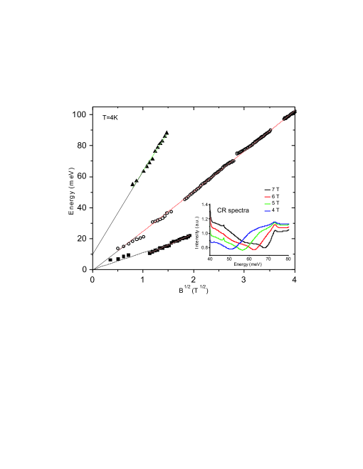
Metamorphic technique of growing InAsSb structuresBelenky11 was recently used for fabrication of InAsSbx/InAsSby short period SLs with band gaps varying from hundreds to 0 meV.Belenky15 Cyclotron resonance (CR) measurements were carried out in a SL with the effective band gap of meV with magnetic field in the growth direction (Faraday geometry).Suchalkin Typical plot of the CR resonance energy vs square root of magnetic field is presented in Fig.1. The energies of the electron CR transition between 0th and 1st Landau levels indicated by the hollow circles are on a straight line passing through the origin. The solid triangles correspond to the transitions between electron and hole Landau levels. The y-intercept of this line gives the effective SL bandgap. The solid squares were interpreted as the electron transitions between 1st and 2nd Landau levels.Ludwig14 This transition vanishes at higher magnetic field due to depopulation of the 2nd Landau level. The linear dependence of the CR resonance energy on is a clear indication on a linear character of the electron dispersion.McClure56 ; Haldane88 ; Jiang07 One can see that the energy range of the electron dispersion linearity starts at 10 meV.
The only analytical theory of electron spectrum in SLs is based on the Kroning - Penney model. (An analytical theory based on Hamiltonian is developed only for narrow band constituent materials.Gerchikov92 ) This model leads to the following equation
| (1) |
where and are the well and barrier width, , and are effective masses in the well and barrier material, and are wave vectors in the growth direction in the well and barrier defined as
| (2) |
is the height of the barrier and is the in-plane wave vector. Eqs.(1) and (2) define the dependence of energy on and quasi wave vector in the growth direction . If then , i.e., the in-plane spectrum is parabolic. Difference of the masses in different layers leads to non-parabolicity of the spectrum. Electron masses in InAs and InSb differ by about two times (, Adachi ; Vurgaftman01 ) and this difference cannot lead to linear in-plane spectrum starting from 10meV.
Another factor that accounts for non-parbolicity of the in-plane spectrum is non-parabolicity of the bulk spectrum in the material of separate layers. It can be described by energy dependence of and . This dependence becomes significant at energies of the order of the band gap in the material of any of SL layers.Kane57 In InAsSb alloys the band gap is larger than 100 meV in the whole range of Sb concentration.Adachi ; Vurgaftman01
The one order of magnitude discrepancy between experimental and theoretical region of parabolic spectrum cannot be related to small inaccuracy of the measurement, Eq.(1) or material constants. It clearly shows that something is wrong with the theory.
III Analysis of the theory
Spectrum of SLs is usually calculated with help of Kronig - Penney model that is periodic system of uniform layers of different material separated with sharp interfaces. Each layer is described with a Hamiltonian in the effective mass approximation and at interfaces carrier wave function fulfills some boundary conditions which meet symmetry limitation and current conservation. Parameters of the Hamiltonian, such as band edge energies, effective masses or Luttinger parameters for valence band are taken equal to their values in corresponding bulk material of the layer. The model gives a simple and comprehensive picture of the spectrum and is widely used.Mukherji75 ; Schulman81 ; Bastard81 ; Smith86 ; Cho87 ; Smith90 ; Ivchenko ; Goncharuk05 ; Qiao12
A cornerstone of this approach is the assumption that method, that is a basis for the effective mass approximation, can be applied to each layer separately leading to layers’ bulk spectrum and SL spectrum can be found based on these results. Some discrepancies between calculated energy levels and their measured valuesMukherji75 ; Schulman81 ; Mailhiot86 can be related to uncertainties in parameters used in the calculation and these uncertainties are really considerable.Adachi ; Vurgaftman01
Primary interest in SL carrier spectrum is typically the spectrum along the growth direction, although the in-plane spectrum is also important for vertical transport because it controls the density of states. Due to separation of growth direction and in-plane variables in each layer the in-plane momentum enters SL dispersion relation as a parameter and the in-plane spectrum can be obtained in a very simple way.Bastard81 ; Ivchenko
The essence of method is that carrier wave functions and spectrum near the band edge are calculated with help of perturbation of the state at the edge. In this paper we assume that the edges of relevant bands are at the center of the Brillouin zone that is true in III-V materials. The starting point of the method is the Hamiltonian in the basis of Bloch wave functions at the center of the zone. At the center where the carrier wave vector the Hamiltonian is a diagonal matrix with diagonal elements equal energies at band edges. Away from the center of the zone kinetic energy of free electron is added to the diagonal elements. Also off-diagonal matrix elements describing coupling between bands are non-zero and proportional to wave vector components and matrix elements of momentum components. The Hamiltonian contains also spin-orbit interaction that is important in III-V crystals.
In the most advanced version of the method, Kane model, the coupling between the conduction and valence band is taken into account exactly while coupling with other bands is considered as a perturbation.Kane57 If this perturbation is neglected the Hamiltonian can be diagonalized exactly. In cubic crystal the spectrum is characterized by only two parameters, matrix element of a momentum component between conduction and valence band (due to cubic symmetry matrix elements of all components are equal) and spin-orbit energy splitting. This Hamiltonian is spherically symmetric and its eigenfunctions are transformed under rotations according to rotation group representations with and . Perturbation by coupling with other bands leads to cubic anisotropy of the valence band that makes the Hamiltonian of the valence band identical to Kohn - Luttinger Hamiltonian.
In SLs only in-plane wave vector is a good quantum number. In the growth direction, unlike bulk, wave functions are not plane waves and new quantum numbers are the number of a subband and quasi wave vector that varies within interval where is the SL period. If and the width of SL layers is much larger than the lattice constant Hamiltonian can be diagonalized in each layer and SL spectrum and wave functions can be obtained with help of appropriate conditions at interfaces between the layers.
If there is an additional part of the Hamiltonian, , proportional to , Eq.(9a). In bulk is equivalent to rotation of the wave vector. If only conduction - valence band coupling is included the rotation does not change the spectrum and new wave functions are obtained with rotational transformation. This procedure does not work in SLs where the symmetry is uniaxial even within separate layers. At small it is possible to consider as a perturbation. Corrections to the spectrum contain (i) matrix elements of between states with and different and (ii) energy difference between these states. These quantities differ from corresponding quantities in bulk because of difference between wave functions and spectrum in the growth direction. Therefore the assumption that the in-plane spectrum in separate layers is the same as in bulk is baseless.
In the next section we consider a new approach to calculation of in-plane spectrum in SLs.
IV equation for superlattice
We study SL spectrum in Kane - type Hamiltonian and for simplicity neglect spin-orbit split band. Then in the basis
| (3) |
the Hamiltonian in each layer is
| (4) |
where is the growth direction, , is the free electron mass, and are energies of the conduction and valence band edge, is the momentum matrix element between the conduction and valence band. In SL with layer width and , , the values of , and are different in different layers,
| (5a) | |||
| (5b) | |||
where is the number of a period.
In Schrödinger equation variables are separated,
| (6) |
and -dependent part of the wave function satisfies the equation
| (7) |
where
| (8a) | |||
| (8b) | |||
| (9a) | |||
| (9b) | |||
| (10) |
Eq.(7) is provided with boundary conditions at interfaces that are limited by symmetry of the wave functions and conservation of current component normal to interfaces. Except boundary conditions there is also Bloch condition
| (11) |
To study solutions to Eq.(7) it is convenient to start with the case of that is reduced to search of eigenfunctions and eigenvalues of . Hamiltonian describes three types of carriers and each of them can be in the ground and excited states. Eigenvalues of are where for electrons, for heavy holes and for light holes. is the number of the subband. Near the edges of subbands the spectrum is parabolic, where corresponds to the subband edge and . All energy levels are double degenerate with respect to spin direction and in correspondence to the block structure of eigenfunctions belonging to are
| (12) |
where
| (13) |
SL quantization brings in new energy scales: energy separation between states with the same but different subband number, the width of subbands and the width of gaps. Except extreme cases all of them are of the order of .
Spectrum resulted from Eq.(7) is formed under the affect of two different factors. One is the in-plane motion described by and the other is superlattice structure described by alternating layers with the boundary condition and Bloch condition. Which one of them is dominant depends on their relative contribution to the spectrum. If the energy scale introduced by , , is larger than then it is possible to consider the superlattice structure as a perturbation and in the leading order to find the spectrum in each layer separately. This is the regular approach. A rough condition of its validity is . Here we consider the opposite case when
| (14) |
and in Eq.(7) can be considered as a perturbation. In-plane spectrum under condition (14) is calculated in the next section.
V In-plane spectrum at small
Eigenfunctions of , , , are orthogonal and normalized,
| (15) |
and solution to Eq.(7) can be expanded in :
| (16) |
Expansion coefficients satisfy the following system of equations
| (17) |
Under condition (14) correction to the spectrum from matrix elements off-diagonal with respect to the band number, , is small and in the leading approximation can be neglected. Then Eq.(17) becomes
| (18) |
and in-plane spectrum in the th subband can be found from the equation
| (19) |
The following calculation is made only for the ground state subband where and to shorten notations subscripts and will be omitted.
Calculation of matrix elements is facilitated by two factors. The first is the block structure of , Eq.(9a), that makes it possible to express them in matrix elements of and :
| (20) |
The second factor is that and the parameter of method in Eq.(13), , in each layer is indeed small because the width of the layers is much larger than the lattice constant. Therefore conduction and valence band mixing is weak in spite of electron and hole masses are strongly different from the free electron mass.111Small parameter of method, , controls valence and conduction band mixing. Correction to the carrier energy resulted from it is . This corresponds to the inverse mass correction that is typically much larger than . In the leading approximation the band mixing of wave functions can be neglected and SL wave functions can be calculated separately for each kind of carriers. So for each kind of carriers matrix function has only one component:
| (21) |
The explicit form of wave functions of electrons , heavy holes and light holes in SL is given in Appendix A. The spectrum can be found from Eqs.(1) and (2) with .
Calculation of blocks of matrix Eq.(20) results in
| (22a) | |||
| (22b) |
where
| (23a) | |||
| (23b) | |||
| (23c) | |||
determinant in Eq.(19) becomes block diagonal after cycle transposition rows and columns (3,4,6). Determinants of the two diagonal blocks are equal so that
| (24) |
That is the spectrum is double degenerate. The free electron energy at practical values of is so small that it can be neglected in Eq.(24).
To study the in-plane spectrum it is convenient to write the dispersion relation in the form
| (25) |
where
| (26) |
There are following relations between these energies
| (27) |
Plot of the left hand side (cubic parabola) and right hand side (straight line) of Eq.(25) as a function of is shown in Fig.2. Crossing points of the curve and straight line correspond to solutions to Eq.(25). The right crossing point corresponds to electrons, the middle crossing point corresponds to heavy holes and the left one corresponds to light holes.
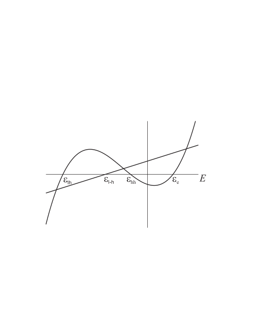
The right hand side of Eq.(25) contains a large parameter: for the most of III-V compounds eV. Vurgaftman01 That is with growth of the prefactor in the right hand side can be quite large when is still small. This prefactor controls the slope of the straight line in Fig.2. With growth of the straight line rotates counterclockwise. The rotation leads to growth of the electron energy and absolute value of the light hole energy without any limitation while the absolute value of the heavy hole energy grows and approaches .
If then asymptotic solution of Eq.(25) at small ,
| (28) |
gives parabolic spectrum:
| (29a) | |||
| for electrons, | |||
| (29b) | |||
| for heavy holes and | |||
| (29c) | |||
for light holes.
A weak nonparabolicity of the electron spectrum at not very large is usually described by energy dependence of the effective mass. In Eq.(29a) this is reduced to replacement of with in the expression for the mass. If the splitting between light and heavy holes is neglected (i.e. assumed to be equal ) and the difference between momentum matrix elements in different layers and is also neglected then the modified expression becomes identical to Eq.(1) of Ref.Wetzel96 where contribution of remote bands and spin-orbit split band is discarded.
At large
| (30) |
the energy of heavy holes is saturated (keep in mind that admixture of remote bands is neglected)
| (31) |
while the spectrum of electrons and light holes is linear
| (32) |
In case interesting for InAsSb SLs, when gap between electrons and heavy holes is anomalously small,
| (33) |
there exists also an intermediate asymptote when
| (34) |
In this energy region the first term in the right hand side of the expression
| (35) |
can be neglected and then Eq.(25) leads to
| (36) |
where the plus corresponds the electron spectrum and minus corresponds to heavy hole spectrum. At small Eq.(36) gives parabolic spectrum Eqs.(29a) and (29b) while at large the spectrum is linear,
| (37) |
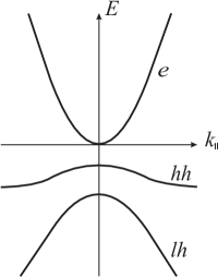
A sketch of the whole in-plane spectrum is shown in Fig.3.
VI Conclusion
Arguments presented in this paper reveal that the in-plane spectrum in SLs at not very large in-plane momentum is not correctly described by the existing theory that uses effective mass approximation in each separate layer. Actually the in-plane spectrum is formed on the top of SL spectrum in the growth direction. The physical reason is that at small the in-plane motion is relatively slow and before an electron makes a noticeable in-plane shift it moves across a few SL periods.
From theoretical point of view when the width of SL layers goes to infinity the SL spectrum has to go to the bulk spectrum. This indeed happens not by decrease of differences between the spectra but by shrinkage of the region of small where these differences are substantial, see Eq.(14).
In practical terms the limitation on from above is not that strong. For period nm and effective mass the energy of the considered region has to be smaller than meV.
The background of the in-plane spectrum is important for the spectrum character because a substantial role in its formation is played by valence - conduction band gap. The value of the gap controls the value of the effective mass, Eq.(29c) [similar calculation in bulk gives ], and the size of the energy region where the spectrum is parabolic. In SL the gap can be significantly smaller than in separate layers. The reason is that the conduction and valence band gap between different layers can be much smaller than the gap in each of them, and , and the SL gap is different from by quantum size effect. This is actually the case in InAsSb SLs.Belenky11 Another example is InAs/GaSb SLs close to type II. If is not small the results of our theory is close to the results of regular approach and may be not distinguishable in experiments.
In this paper we are not trying to explain results of the cyclotron measurements presented in Sec.II. This is going to be done elsewhere. We can just make a rough estimate of energy difference between electron Landau levels based on the results obtained in Sec.V. To obtain such an estimate we make use of Eq.(37) and choose plus sign for electron levels. A rough value of Landau level energy can be obtained by replacing with where is magnetic field and is the number of the level. This leads to linear dependence of the cyclotron resonance energy on . Making use of known value eV Vurgaftman01 we obtain for the transition between the first and second Landau levels meV/ that is close to the slope 10 meV/ of the lowest line in Fig.1.
Finally, the results of the work can be summarized in the following points:
-
•
The size of the parabolic region in the in-plane spectrum is of the order of the conduction - valence band gap of the SL.
-
•
The value of the effective mass is inverse proportional of the SL band gap.
-
•
Beyond the parabolic region the electron and light hole spectrum is linear.
-
•
If the gap between heavy holes and conduction band is much smaller than the gap between light holes and conduction band linear spectrum of the electron and heavy holes starts at the energy around the smaller gap.
-
•
The size of the parabolic region of the spectrum and its linearity beyond this region are consistent with recent CR measurements. A rough estimate of the cyclotron resonance energy gives a value close to the experimentally measured one.
VII Acknowledgements
We appreciate very helpful discussions with L. D. Shvartsman. The work was supported by U.S. Army Research Office Grant W911TA-16-2-0053.
Appendix A SL wave functions
We calculate SL wave functions in the frame of regular Kronig - Penney model. Let the barrier height is and effective masses in well and barrier are and . Schrödinger equation
| (38a) | |||
| (38b) | |||
where is the width of the well, is the width of the barrier, , with boundary conditions
| (39a) | |||
| (39b) | |||
and Bloch condition
| (40) |
leads to well known dispersion law, Eq.(1), and wave functions
| (41a) | |||
| (41b) | |||
| (42) |
Two constants and can be expressed in only one:
| (43a) | |||
| (43b) | |||
and the normalization condition
| (44) |
gives the following relation between the constants
| (45) |
All relations in this Appendix are equally valid for and , i.e., for real and imaginary .
Wave functions of electrons, heavy holes and light holes differ by values of effective masses, the height of the barrier and the width of the wells and barriers: layers presenting wells for electrons are barriers for hole and the other way around.
References
- (1) G. Belenky, Y. Lin, L. Shterengas, D. Donetsky, G. Kipshidze and S. Suchalkin, Electron. Lett. 51, 1521 (2015).
- (2) J. G. Crowder, H. R. Hardaway, and C. T. Elliott, Meas. Sci. Technol. 13, 882 (2002).
- (3) N. V. Zotova, N. D. Il’inskaya, S. A. Karandashev, B. A. Matveev, M. A. Remennyi, and N. M. Stus’, Semiconductors 40, 697 (2006).
- (4) E. J. Koerperick, D. T. Norton, J. T. Olesberg, B. V. Olson, J. P. Prineas, and T. F. Boggess, IEEE J. Quantum Electron. 47, 50 (2011).
- (5) S. Suchalkin, G. Belenky, D. Smirnov, S. Moon, B. Laykhtman, L. Shterengas, G. Kipshidze, M. Ermolaev, to be published.
- (6) G. Bastard, Phys. Rev. B 24, 5693 (1981); 25, 7584 (1982).
- (7) D. F. Welch, G. W. Wicks, and L. F. Eastman, J. Appl. Phys. 55, 3176 (1984).
- (8) T. Hiroshima and R. Lang, Appl. Phys. Lett. 49, 456 (1986).
- (9) D. F. Nelson, R. C. Miller, and D. A. Kleinman, Phys. Rev. B 35, 7770 (1987).
- (10) K. H. Yoo, L. R. Ram-Mohan and D. F. Nelson, Phys. Rev. B 39, 12808 (1989).
- (11) C. Wetzel, R. Winkler, M. Drechsler, B. K. Meyer, U. Rössler, J. Scriba, J. P. Kotthaus, V. Härle and F. Scholz, Phys. Rev. B 53, 1038 (1996).
- (12) M. J. Yang, P. J. Lin-Chung, B. V. Shanabrook, J. R.Waterman, R. J. Wagner and W. J. Moore, Phys. Rev. B 47, 1691 (1993); M. J. Yang, R. J. Wagner, B. V. Shanabrook, J. R. Waterman and W. J. Moore, Phys. Rev. B 47, 6708 (1993).
- (13) J. Scriba, A. Wixforth, J.P. Kotthaus, C. Bolognesi, C. Nguyen, and H. Kroemer, Solid State Comm. 86, 633 (1993).
- (14) R. Winkler, Surf. Sci. 361/362, 411 (1996).
- (15) L. G. Gerchikov, G. V. Rozhnov, and A. V. Subashiev, Sov. Phys. JETP 74, 77 (1992) (Zh. Eksp. Teor. Fiz. 101, 143 (1992)).
- (16) S. Adachi, Physical Properties of III-V Semiconductor Compounds (John Wiley & Sons, New York 1992); Handbook on Physical Properties of Semiconductors, Vol. 3 II-VI Compound Semiconductors (Kluwer Academic Publisher, New York 2004).
- (17) I. Vurgaftman, J. R. Meyer and L. R. Ram-Mohan, J. Appl. Phys. 89, 5815 (2001).
- (18) B.Laikhtman, S. de-Leon, and L.D.Shvartsman, Solid State Commun. 104, 257 (1997).
- (19) A. V. Rodina, A. Yu. Alekseev, Al. L. Efros, M. Rosen and B. K. Meyer, Phys. Rev. B 65, 125302 (2002)
- (20) M. Altarelli, Phys. Rev. B 28, 842 (1983); Physica B 117 & 118, 747 (1983); M. Altarelli, U. Ekenberg and A. Fasolino, Phys. Rev. B 32, 5138 (1985).
- (21) D. L. Smith and C. Mailhiot, Phys. Rev. B 33, 8345 (1986); C. Mailhiot and D. L. Smith, Phys. Rev. B 35, 1242 (1987); D. L. Smith and C. Mailhiot, Rev. Mod. Phys. 62, 173 (1990).
- (22) G. Y. Wu and T. C. McGill, Appl. Phys. Lett. 47, 634 (1985); Y. Rajakarunanayake, R. H. Miles, G. Y. Wu, and T. C. McGill, Phys. Rev. B 37, 10212 (1988)
- (23) C. Mailhiot and D. L. Smith, Phys. Rev. B 33, 8360 (1986).
- (24) A. Zakharova, S. T. Yen and K. A. Chao, Phys. Rev. B 64, 235332 (2001); 66, 085312 (2002).
- (25) P. C. Klipstein, Phys. Rev. 81, 235314 (2010); Y. Livneh, P. C. Klipstein, O. Klin, N. Snapi, S. Grossman, A. Glozman, and E. Weiss, Phys. Rev. B 86, 235311 (2012); P.C. Klipstein, Y. Livneh, O. Klin, S. Grossman, N. Snapi, A. Glozman, E. Weiss, Infrared Physics & Technology 59, 53 (2013).
- (26) P.-F. Qiao, S. Mou, and S. L. Chuang, Optics Express 20, 2319 (2012).
- (27) M.-F. S. Tang and D. A. Stevenson, Appl. Phys. Lett 50, 1272 (1987).
- (28) J.-C. Lee, T. E. Schlesinger and T. F. Kuech, J. Vac. Sci. Technol. B 5, 1187 (1987).
- (29) U. Egger, M. Schultz, P. Werner, O. Breitenstein, T. Y. Tan, and U. Gösele, R. Franzheld, M. Uematsu and H. Ito, J. Appl. Phys. 81, 6057 (1997); S. Senz, U. Egger M. Schultz, U. Gösele and H. Ito, J. Appl. Phys. 84, 2546 (1998).
- (30) M. R. Wood, K. Kanedy, F. Lopez, M. Weimer, J. F. Klem, S. D. Hawkins, E. A. Shaner, J. K. Kim, J. Crystal Growth 425, 110 (2015).
- (31) G. Belenky, D. Donetsky, G. Kipshidze, D. Wang, L. Shterengas, W. L. Sarney, and S. P. Svensson, Appl. Phys. Lett. 99, 141116 (2011).
- (32) J. Ludwig, Yu. B. Vasilyev, N. N. Mikhailov, J. M. Poumirol, Z. Jiang, O. Vafek, and D. Smirnov, Phys. Rev. B 89, 241406(R) (2014).
- (33) J. W. McClure, Phys. Rev. 104, 666 (1956).
- (34) F. D. M. Haldane, Phys. Rev. Lett. 61, 2015 (1988).
- (35) Z. Jiang, E. A. Henriksen, L. C. Tung, Y.-J. Wang, M. E. Schwartz, M. Y. Han, P. Kim, and H. L. Stormer, Phys. Rev. Lett. 98, 197403 (2007).
- (36) E. O. Kane, J. Phys. Chem. Solids, 1, 249 (1957); The kp Method, in Semiconductors and Semimetals, Eds. R. K. Willardson and A.C. Beer (Academic Press, New York 1966) Vol. 1, p.75.
- (37) D. Mukherji and B. R. Nag, Phys. Rev. B 12, 4338 (1975).
- (38) J. N. Schulman and Y.-C. Chang, Phys. Rev. B 24, 4445 (1981).
- (39) H.-S. Cho and P. R. Prucnal, Phys. Rev. B 36, 3237 (1987).
- (40) D. L. Smith and C. Mailhiot, Rev. Mod. Phys. 62, 173 (1990).
- (41) E. L. Ivchenko and G. E. Pikus, Superlattices and Other Heterostructures (Springer 1995).
- (42) N. A. Goncharuk, L. Smrc̆ka, J. Kuc̆era, and K. Výborný, Phys. Rev. B 71, 195318 (2005).
Figure cations
Fig.1: Absorption peaks energies vs magnetic field for 1m thick InAsSb0.3 (4nm)/InAsSb0.75(2nm) SL. The magnetic field is parallel to the growth direction. Lines display the best fit to the data points. Insert: electron CR peaks at different magnetic fields.
Fig.2: The curve is the plot of the left side of Eq.(25) and the straight line is the plot of the right hand side. Their crossing points correspond to solutions to the equation.
Fig.3: A sketch of the in-plane spectrum of electrons, heavy holes and light holes.